Ghodssi R., Lin P., MEMS Materials and Processes Handbook
Подождите немного. Документ загружается.

844 S.J. Cunningham a nd M. Kupnik
would need to be introduced. These are known processes that could be introduced.
Following the s puttered Pyrex deposition, electrical vias are wet etched (Fig. 11.13c)
and filled with an evaporated Cr/Au/Pt contact metallization (Fig. 11.13d). A sili-
con microstructure is fabricated in parallel (not shown) and separately bonded to
this interconnect substrate (Fig. 11.13e).
The FMI process was a three-wafer process that included the Pyrex intercon-
nect/electrode substrate and a silicon device wafer that included an n-device layer, a
p+ etch stop layer, and an n–handle wafer. Each of the three wafers included shared
unit process steps, but they could be processed independently and in parallel. During
early production, it was found that the manual anodic bonder was a bottleneck in the
fabrication production flow. This occurred because two anodic bonding steps were
performed for each completed device. The first anodic bond was formed between the
device wafer and the Pyrex substrate. The second anodic bond was formed between
the Pyrex substrate, including the bonded device, and a silicon lid. The bottleneck
was eliminated by adding an automated bonding system that included an alignment
station, robot, and bonding station. This is just a reminder as you consider moving
your wafer-level encapsulation process into production. The third wafer was a sili-
con wafer ((100) n-silicon) used as the lid (Fig. 11.13g). The first step was to deposit
Si
x
N
y
on both sides of the wafer and pattern one side, such that the Si
x
N
y
acted as a
masking layer for a KOH etch (Fig. 11.13h). The KOH etch formed a 100 μm deep
cavity to provide a volume for the MEMS device and to provide standoff height for
the sawing process to expose the bond pads (Fig. 11.13i).
At this point the silicon wafer could be stored until needed for a mating wafer,
when the silicon nitride is stripped so the silicon wafer can be bonded to the Pyrex
wafer. On consideration with this particular stack is the thermal mismatch between
the silicon wafer and the Pyrex wafer. This bonding process was performed at 300 V
and 315
◦
C, where there is only a small difference in the CTEs of the two materials.
The silicon lid is shown bonded to the Pyrex wafer including the MEMS devices
in Fig. 11.13i.InFig.11.13j, a contact is deposited and patterned on top of the lid
for electrical connection. In subsequent assembly processes, it was possible to wire
bond to the contact on top of the lid further demonstrating the robustness of the
bond. During the wafer sawing process, the first saw cuts partially saw through the
silicon wafer to expose the bond pads. With the bond pads exposed, a wafer-level
electrical test was performed to identify known the good die and verify functionality.
After the functional test, the sawing process was completed to singulate the die,
which did not affect the integrity of the bond (Fig. 11.13k).
The packaged accelerometer product is shown in Fig. 11.14 at three levels of
assembly. The wafer-level encapsulated silicon accelerometer is epoxy mounted to a
Kovar lead frame. On the same lead frame paddle and adjacent to the accelerometer
die i s the Delta–Sigma modulator ASIC that is used to convert the capacitance signal
for the accelerometer to a digital signal using the airbag deployment module. The
accelerometer die is wire bonded to the ASIC for sensing purposes and the ASIC
is wire bonded to the package pins. Figure 11.14a shows a lead frame strip with
several accelerometer and ASIC die mounted to the lead frame and ready for the next
processing steps. A close-up image of the accelerometer die is shown in Fig. 11.14b,
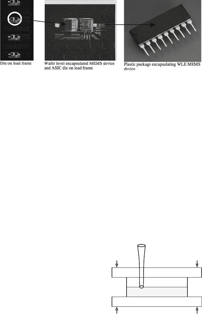
11 Wafer Bonding 845
(a) (b) (c)
Fig. 11.14 MEMS device shown with hermetic wafer-level encapsulation and low-cost, molded
plastic package
where the silicon lid can be seen bonded to the Pyrex substrate. In Fig. 11.14c,the
lead frame, accelerometer die, and ASIC die have been plastic over molded to form
a hermetic package. The package is hermetic because t he silicon lid anodic bonded
to the Pyrex substrate is hermetic. Without the ability to form a hermetic bond by
anodic bonding of a silicon wafer to a Pyrex substrate, this hermetic accelerometer
in a low cost plastic over molded package would not be possible.
11.2.6 Silicon–Glass Laser Bonding
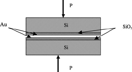
Wild et al. [37] produced strong reproducible bonds between polished silicon and
Pyrex wafers by laser bonding. The silicon and glass wafers are compressed together
between two plates as shown in Fig. 11.15. One of the plates is transparent to the
incident laser light, which needs to impinge upon the glass–silicon interface. They
used a fiber-coupled, Nd:YAG laser (λ = 1064 nm) with a power of 15–30 W
with a laser scan velocity of 100–400 mm/min. They demonstrated bond spots and
lines up to 300 μm wide. The compressive load ranged from 10 to 30 MPa. They
found the hot zone was small and self-limiting by temperature-dependent thermal
Glass
Glass
Silicon
Base
Laser
F
Fig. 11.15 Basic
silicon–glass laser bonding
process
846 S.J. Cunningham a nd M. Kupnik
absorption and conductivity. The absorption increases and conductivity decreases
with increasing temperature. It is typical for the temperature outside the hot zone to
be 150–250
◦
Cfor<2s.
11.3 Wafer Bonding with Intermediate Material
11.3.1 Thermocompression Bonding
Tsau et al. [38] have characterized the fabrication of wafer-level thermocompres-
sion bonds, which can be described and the solid-state welding of two surfaces
with applied heat and pressure. The bonding material of choice is Au because it is
oxidation resistant, has a low yield point, is corrosion resistant, has a high electri-
cal conductivity, is an hermetic seal, and SiO
2
can be used as a diffusion barrier
between silicon and Au. The typical bonding temperature is 300
◦
C, which is m uch
lower than fusion bonding at 800
◦
C and on the order of anodic bonding at roughly
300
◦
C. The applied pressure between the two wafers is 7 MPa. It was found that
1500 Å of SiO
2
provides an adequate diffusion barrier between Si and Au. The crit-
ical strain energy release rate was determined to be 22–67 J/m
2
, which is largely
independent of the Au bond layer thickness for a thickness range of 0.23–1.4 μm.
A simple view of the process is shown in Fig. 11.16.
Fig. 11.16 Wafer-level
thermocompression bonding
11.3.2 Eutectic Bonding
The most common eutectic bond formed is between Au and Si as described by
Wolffenbuttel and Wise [39], but Au–In eutectic bonds are being developed for
lower temperature bonding. The Au–Si eutectic point is 363
◦
C, which is maintained
for about 40 min. The Au usually includes an adhesion layer such as Cr or Ti and
a diffusion barrier such as Pt. In Fig. 11.17, two examples of Au–Si eutectic bond
constructions are shown. In the first flow an SOI wafer with a silicon handle wafer,
SiO
2
isolation layer, and a silicon device layer is bonded to a silicon wafer with a
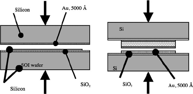
11 Wafer Bonding 847
Fig. 11.17 Au–Si and Au–In eutectic bonding
5000 Å Au layer. In a second implementation, the first wafer is a silicon wafer with
aSiO
2
diffusion barrier (prevent diffusion between Au and Si), and a 5000 Å Au
layer (including a 150 Å Cr adhesion layer). The second silicon wafer includes a
SiO
2
isolation layer, a 150 Å Cr adhesion layer, 1100 Å Au (AuIn
2
) layer, followed
by a 6 μm indium bonding layer, and concluding with a 1500 Å (AuIn
2
) layer to
prevent indium oxidation. The Au–In bonding process is performed at 250
◦
Cfor
15 min with a 2 kgf force. The Au–In bonding temperature of 250
◦
C is significantly
lower than the Au–Si eutectic of 363
◦
C.
11.3.3 Polymer Bonding
Niklaus et al. [9, 40–42] have written an excellent review of adhesive wafer bond-
ing and demonstrated the general application of adhesive bonding. Their purpose
was to describe the importance of adhesive wafer bonding that uses an intermediate
polymer layer to bond two substrates. The adhesive is applied to a surface of one
or both wafers. The typical method of application is by spin coating for thickness
uniformity. The wafers are joined together by the application of pressure. Finally,
heat or UV light is applied to convert the adhesive from a liquid or viscoelastic state
to a solid state. Adhesive bonding is often chosen for the following advantages: low
bonding temperature (RT to 450
◦
C); compatibility with CMOS wafers; compati-
bility with a high degree of surface roughness or topography; compatibility with
various wafer materials, including silicon, GaAs, glass (Pyrex, Hoya), Sapphire,
and InP to InGaAsP [43], compatible with various surface conditions relative to
cleanliness. Because adhesive bonding can accommodate various degrees of sur-
face roughness, topography, and even contamination, it does not require special
treatments such as planarization, chemical-mechanical polishing, or cleaning. On
the other hand, the polymers are not stable over a wide temperature range, cannot

848 S.J. Cunningham a nd M. Kupnik
survive in various harsh environments that include solvents, and do not provide
hermetic bonds against gases or moisture. In many cases the polymer or adhesive
bond materials are used for temporary bonds [44].
A list of polymers used in adhesive bonding is given in Table 11.1 showing
four general material classes including thermoplastics such as Parylene [45–47],
thermosets, elastomers, and hybrids. A thermoplastic has the characteristics of solid-
ifying upon cooling and can be remelted. Thermoset materials experience significant
cross-linking that forms a three-dimensional bond network and cannot be remelted
or reshaped. The elastomeric materials can sustain a large deformation with low
stress (5–10x the unstretched dimension).
Table 11.1 Polymers used in wafer bonding
Polymer material Characteristics
Epoxies Thermosetting
Thermal and two component curing
Strong and chemically stable
UV epoxies (Su8) Thermosetting
UV curable (if one substrate is UV transparent)
Strong and chemically stable
Bondable with patterned films
Positive photoresists Thermoplastic
Hot melt
Void formation at the interface
Weak bonds
Negative photoresists Thermosetting
Thermal and UV curable
Weak bond
Low thermal and chemical stability
Bondable with patterned films
BCB (benzocyclobutene) Thermosetting
Thermal curable
High assembly yield
Strong bond
Thermally and chemically stable
Bondable with patterned films
Flare Thermosetting
Thermal curable
High assembly yield
Bondable with patterned films
PMMA (polymethylmethacrylate) Thermoplastic
Hot melt
PDMS (polymethylsiloxane) Elastomeric materials
Thermal curing
Fluoropolymers Thermoplastic and thermosetting
Thermal curable or hot melt
Chemically stable
Bondable with patterned films

11 Wafer Bonding 849
Table 11.1 (continued)
Polymer material Characteristics
Polyimides Thermosetting and thermoplastics
Thermal curing and hot melt
Voids form during imidization process
Wafer/chip scale process
Bondable with patterned films
MSSQ (methylsilesquioxane) Thermosetting
Thermal curing
Strong
Chemically and thermally stable
Void formation during curing
PEEK (polyetherketone) Thermoplastic materials
Hot melt
ATSP (thermosetting copolyesters) Thermosetting
Thermal curing
PVDC (thermoplastic copolymers) Thermoplastic
Hot melt
Parylene Thermoplastic
Hot melt
LCP (liquid crystal polymer) Thermoplastic material
Hot melt
Very good moisture barrier
Waxes Thermoplastic
Hot melt
Low thermal stability
Temporary bonding
From Niklaus et al. [9]
The typical process steps for adhesive wafer bonding include: (1) cleaning
and drying the wafers; (2) treating the wafer surface with an adhesion promoter;
(3) application of the polymer adhesion layer to one or both of the wafers; (4) a
soft bake for partial curing of the adhesive; (5) wafers are placed in a bond chamber
where they are aligned and contact established; (6) an external load or pressure is
applied to the wafer stack; (7) the adhesive is remelted or cured during the pres-
sure loading; and (8) the wafers are cooled, the pressure removed, and the wafers
removed from the bonding chamber.
The cleaning and drying process is intended to remove particles, surface contam-
inants, and moisture from the wafer surfaces. Adhesion promoters may be needed
with some polymers and some materials. They are intended to change the surface
state of the wafer and enhance adhesion between the wafer and the polymer. The
polymer is applied to the wafer surfaces by spraying, electrodeposition, stamping,
screen printing, brushing, and dispensing of liquid precursors. The most common
method in MEMS and electronic fabrication is spin coating. The viscosity of the
liquid precursor and the spin speed of the wafer determine the resulting thickness
and will result in highly uniform thickness and smooth surfaces. Polymer adhesive
thicknesses have been achieved between 0.1 and 100 μm. In addition, the polymer

850 S.J. Cunningham a nd M. Kupnik
can be patterned so that the polymer bonds to a limited area of the mating wafer.
A softbake is performed to remove solvents and other volatiles from the polymer
material. Thermosetting materials are not or partially polymerized during the pre-
bake. Thermoplastic materials can be completely polymerized because they can be
remelted during the bonding process.
The wafers are commonly joined in a vacuum chamber to prevent voids and
trapped gases from being formed at the bond interface. It is necessary to be able
to pump away the trapped gases before the bond is initiated. During the pressure
loading steps, thermosetting polymers should be at the bonding pressure before
the curing temperature is reached because the polymerization is not reversible.
With thermoplastic materials, the bond pressure can be reached after the bonding
temperature is achieved. The remelting and curing of the adhesive occurs at the
bonding temperature. At the end of the bonding process, the sequence of chamber
purge, release of bonding pressure, and cooldown depend on the type of poly-
mer. With thermoplastics, the wafers should be cooled before the bonding pressure
is released so that the polymer is hardened and solidified before the pressure is
released. In Table 11.2, a process is outlined for the thermosetting polymer BCB
(benzo-cyclo-butene) [48].
Table 11.2 Typical BCB bonding process
Process step Processing parameters
Cleaning
Adhesion promoter
Polymer application Spin coating on one or both wafers
Softbake T = 100 − 170
◦
C, t = few minutes
Atmosphere 10
−3
mbar
Bonding pressure P
B
= 0.2 − 0.5 MPa
Curing temperature T
B
= 200 − 300
◦
C
Bonding time t = t(T
B
) − t = 1 h at 250
◦
C
In the continued pursuit of lower temperature encapsulation processes, bonding
processes have been developed using epoxy or BCB bonding. This type of bonding
is consistent with many IC packaging alternatives. Some of the advantages of epoxy
bonding include low cost, an established process for packaging, and low tempera-
tures (60–200
◦
C). It is insulating so t hat it can be bonded directly to RF circuits or
transmission line. Because it is insulating it can work with through wafer or surface
transmission lines, which pass through the bond area. Two concerns associated with
organic bonds are hermeticity/leak rates and outgasing contamination. Leak rates of
10
−7
cc/sec have been achieved with epoxy and gross leak by BCB. The outgasing
can change the encapsulated environment, leave films that cause in-use stiction and
reduce lifetime, or more specifically reduce the reliability of switch contacts.
A simple example of BCB bonding is shown where the substrate and lid wafer
can be either silicon or glass, with the BCB applied to one of the wafers as shown
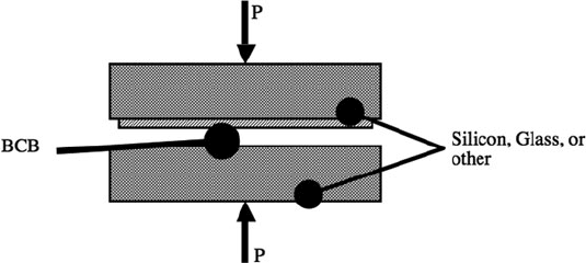
11 Wafer Bonding 851
Fig. 11.18 BCB bonding schematic
in Fig. 11.18. The BCB is a photosensitive, patternable material. It has a low loss
tangent: 8 × 10
−4
to 2 × 10
−3
for 1 MHz to 10 GHz. It has a high resistivity and
low dielectric constant of 2.65. During the processing, pressure and temperature are
needed. A typical bonding pressure is 250 gf. The BCB flows at a temperature of
170
◦
C and cures at 250
◦
C.
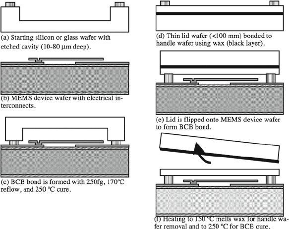
Jourdain et al. [49] demonstrated wafer-level packaging of RF MEMS devices
using BCB bonding with both thick and thin (<100 mm) lid wafer processes.
Using the BCB material allowed the implementation of coplanar RF transmission
lines under the BCB seal ring rather than developing through wafer intercon-
nect/transmission line processes. The BCB process is a low temperature process
where the BCB reflows at 150
◦
C and cures at 250
◦
C. To achieve the RF perfor-
mance, low-loss, high-resistivity lid materials are used and the cavity height should
exceed 1/3 CPW width with the high resistivity silicon. The BCB process was
demonstrated with a thick lid wafer that was formed from silicon or glass. A cavity
is etched 10–80 mm into the lid wafer that is approximately 650 mm thick as shown
in Fig. 11.19a. The BCB is spin coated and patterned on the wafer to a thickness of
3–10 mm. The lid wafer can be diced into individual die and bonded to a device die
or the lid wafer can be bonded to the device wafer (Fig. 11.19b). In this case, a die
level bond is described using s tandard flip-chip bond equipment. The lid is flipped
to mate the BCB seal ring to the device wafer as shown in Fig. 11.19c. The BCB
bond was formed with an applied force of 250 gf, at a reflow temperature of 170
◦
C,
and a cure temperature of 250
◦
C.
The thin lid wafer process was developed as a low-profile encapsulation process.
The lid wafer is less than 100 μm thick and is handled by bonding the thin lid wafer
to a handle wafer using wax (Fig. 11.19d). With the lid wafer bonded to the handle
wafer, the BCB is spin coated and patterned to form the seal ring at a thickness of
3–10 μm. As in the previous case, the thin lids are sawn into individual lids that are
flip-chipped onto the MEMS die to form the seal (Fig. 11.19e). The wafer is heated
to 150
◦
C to melt the wax to remove the handle wafer and cure the BCB material as
shown in Fig. 11.19f. The lidded MEMS device wafer is sawn into individual die
after lidding.
852 S.J. Cunningham a nd M. Kupnik
Fig. 11.19 BCB bonding for thick and thin wafers
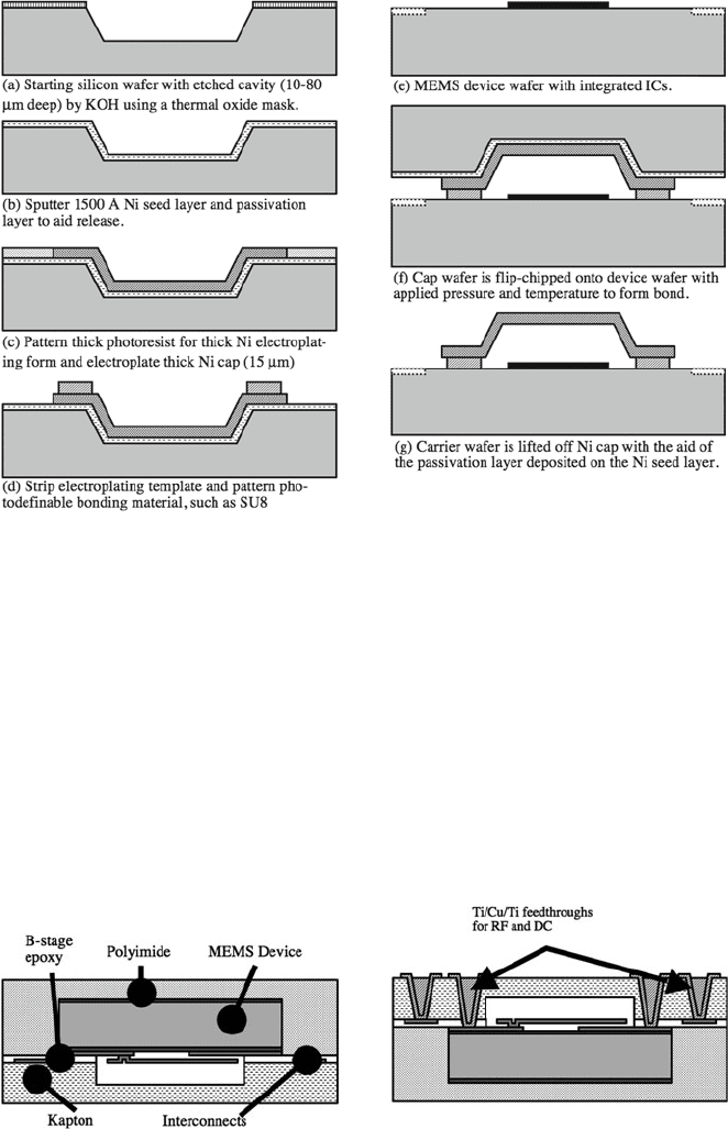
A second example of low-temperature organic bonding for micropackaging is
the microcap packaging process described by Pan [50]. In this process a silicon car-
rier wafer (100) is used as a lid form, which typically has a thickness of 525 μm
with a 1.5 μm thick thermal oxide (Fig. 11.20a). The microcap form is etched into
the silicon using a 30% wt solution of KOH at 70
◦
C using the thermal oxide as
an etch mask as shown in Fig. 11.20b. The thermal oxide etch mask is removed
before a 1500 Å Ni seed layer and passivation layer are sputter deposited as shown
in Fig. 11.20c. A thick photoresist is deposited and patterned for electroplating the
thick Ni (15 mm) cap structure shown in Fig. 11.20d.InFig.11.20e, a photopat-
ternable bonding material is deposited, solvents evaporated and developed, and the
electroplating template is stripped. The cap wafer is now ready to be flip-chipped
onto the device wafer as shown in Fig. 11.20f. The bond was formed using a com-
bination of force, temperature, and materials. Once the bond is formed the carrier
wafer is removed to leave the Ni cap bonded to the device wafer (Fig. 11.20g). The
Ni seed layer passivation is needed to be able to separate the carrier wafer from the
Ni cap.
The bonding strength was measured and found to be maximized between 80 and
120
◦
C. SU8 had the highest bond strength rated at 213 kg/cm
2
and 90
◦
C. Other
bonding layers included AZ-4620 (86 kg/cm
2
at 90
◦
C), SP-341 (100 kg/cm
2
at
90
◦
C), and JSR (88 kg/cm
2
at 90
◦
C). The bond strength increased with increasing
bond force and the authors recommended a minimum bond force of 50 N. The glass
11 Wafer Bonding 853
Fig. 11.20 Microcap packaging process using Ni cap and photodefinable bonding material
transition temperature of the bond material limits the bonding temperature from 115
to 180
◦
C.
A final example of an encapsulation process using epoxy and other organic mate-
rials has been developed. The process begins with a completed MEMS device and
substrate that can be 8–10 in. glass, silicon, or GaAs wafers. The MEMS device die
is flipped (device down as shown in Fig. 11.21a) and bonded to Kapton film using
a B-stage epoxy. The Kapton has a cavity to house the MEMS device and includes
the transmission lines for the RF signals. At this point the MEMS die is encapsu-
lated in polyimide. The polyimide is etched to create vias for interconnection of the
RF I/O and DC control lines. The vias are metallized with Ti/Cu/Ti as shown in
Fig. 11.21 Encapsulation process using Kapton, polyimide, and vertical feedthroughs
