Ghodssi R., Lin P., MEMS Materials and Processes Handbook
Подождите немного. Документ загружается.

834 S.J. Cunningham a nd M. Kupnik
2 cm
wafers get aligned
at these two edges
by gravity
for applying force
at the center
downward
slope
for pick-up with
tweezers
groove that collects
particles and for well
ned edges
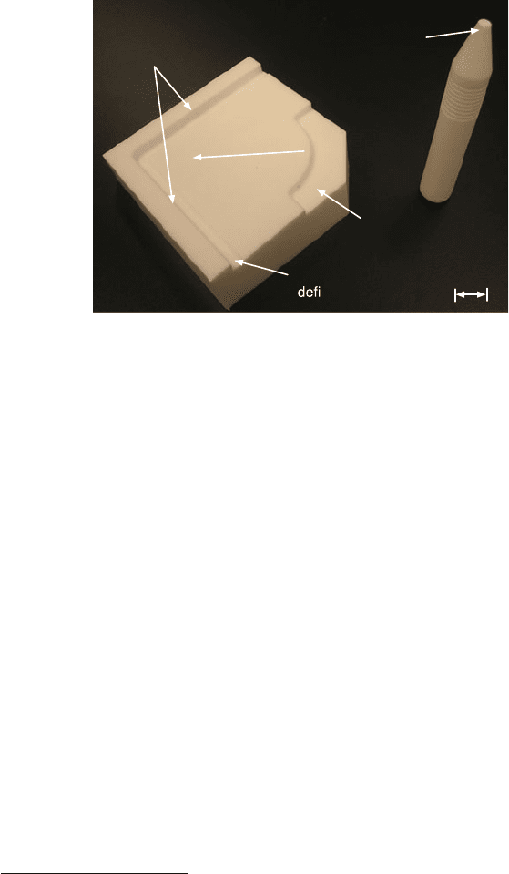
Fig. 11.8 Very useful tool for direct hand bonding available a t the Stanford Nanofabrication
Facility. This version is for 4 in. wafers and made of polytetrafluoroethylene (Teflon). It was
designed by Dr. Aaron Partridge, SiTime Corporation, Sunnyvale, CA, and machined by Karlheinz
Merkle, Machine Shop Supervisor at Department of Physics, Stanford University
at the Stanford Nanofabrication Facility. Because it is made from Teflon it can be
cleaned regularly in a diffusion clean wet bench.
However, often a commercially available bonding tool will be required or pre-
ferred. A description of commercially available tools with more information can be
found in Section 11.8.2. There are several reasons why a bonding tool is inevitable
or advantageous for many MEMS processes. For example:
• Requirement for good alignment between top and bottom wafer. Several microm-
eters down to 200 nm are possible
4
on 300 mm wafers between the top and
bottom wafer.
• Another reason is the necessity of evacuating cavities during the wafer bonding
step. In that case the direct bonding step needs to be performed in vacuum or in a
different atmosphere. A good example for the vacuum requirement is the fabrica-
tion of wafer-bonded capacitive micromachined ultrasonic transducers (CMUTs),
first demonstrated by [2].
• State-of-the-art bonding tools provide further advantages such as reproducible
bonding conditions (temperature, pressure, force, etc.); the ability to activate, dry,
and preclean the surfaces in the bonder itself; and high-end models support auto-
matic operation for better throughput. At the end of this chapter we discuss the
4
Most customers today specify a 1–3 μm alignment requirement for their bonding applications.
Only the latest high-end tools support low alignment tolerances down to 200 nm (personal email
exchange with Jim Hermanowski, from SUSS MicroTec Inc.). The market for such systems
is focused on 3-D IC fabrication, such as high-density memories (SRAM, DRAM, Flash), RF
technologies, and the like.
11 Wafer Bonding 835
operation principle of such bonding tools, which support many different methods
for wafer bonding, in more detail.
• As a general rule, one can say that the likelihood for successful direct wafer
bonding is higher when bonding tools are used. Furthermore, a better bond qual-
ity can be expected as well. Many times, however, direct bonding by hand can
be advantageous for certain MEMS applications, because of the low cost (no
tool purchase) and the short time required to bond wafers by hand compared to
bonding tools.
11.2.4.3 Basic Operation Principle of a Wafer Bonding Tool
The basic operation principle of a bonding tool is explained (simplified) as follows
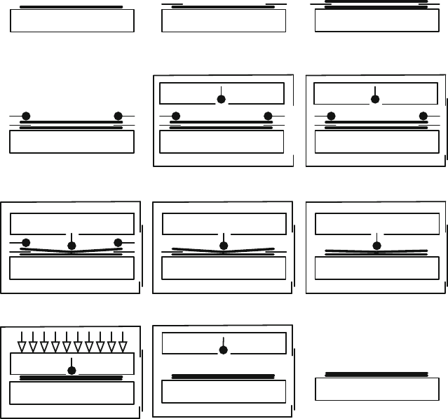
(see Figs. 11.9 and 11.10):
The first wafer, with cleaned and activated bonding surface facing upwards, is
put on the chuck of the bonding tool (Fig. 11.9a). An exemplary photograph of a
(e) (f)(d)
(b) (c)(a)
(h) (i)(g)
(k) (l)(j)
Fig. 11.9 Exemplary sequence of steps (simplified) of how a bonding tool bonds two wafers
836 S.J. Cunningham a nd M. Kupnik
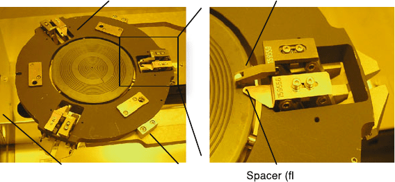
ag)
Wafer clamp
Loading arm
Bond chuck (4 inch)
Bonding chamber
Fig. 11.10 Exemplary photograph of a chuck (hand alignment only) of a wafer bonder (Model
SB6 from SUSS MicroTec AG, Germany). Pictures were taken at the Stanford Nanofabrication
Facility, Stanford, CA. There are many different chucks (for alignment, for various wafer sizes,
and for pieces) available
chuck with spacers and wafer clamps i s shown in Fig. 11.10. Then thin spacers, also
called flags (∼150 μm thick) are positioned on top of this wafer at the outermost
perimeter, that is, a few mm into the wafer area only (Fig. 11.9b). After that, the
second wafer, with the bonding surface facing downwards, is carefully placed on top
of these spacers (Fig. 11.9c), before wafer clamps are attached to hold this s tack in
place (Fig. 11.9d). It can be recommended to use an N
2
gun, equipped with a particle
filter, before placing the top wafer to ensure that no particles are present between
the wafers. Note that the steps so far can be performed in a regular alignment tool
as well for aligned wafer bonding, but then a compatible wafer chuck is required.
The next step is to open the purged chamber of the wafer bonding tool and load in
the chuck (Fig. 11.9e).
After the chamber is closed, the pump down and heating cycle is initiated
(Fig. 11.9f). Most bonders allow heating the top and bottom fixture, which will
be in contact with the chuck and the wafer stack, inside the bonder independently
(∼up to 500
◦
C). After the target vacuum level (e.g., 10
−5
mbar) is reached a pin or
membrane is used to apply some force in the center of the wafer stack (Fig. 11.9g),
as one would do during bonding by hand as well. At that stage the bond wave can-
not propagate far because the spacers are still positioned between the wafers. The
wafers are constrained in terms of any movement, and, thus, the wafer clamps can
be removed (Fig. 11.9h). Then the spacers are pulled out (Fig. 11.9i) and the bond
wave can propagate over the entire surface, as was the case i n (Fig. 11.2). The center
pin or membrane is still in contact with the wafers, but in addition, now the tool has
space to move the top fixture down (Fig. 11.9j) and can apply a considerable amount
of force (e.g., 1000 N for direct bonding), depending on the type of bonding that is
performed.
In the case of anodic bonding (Section 11.2.5), an electrical voltage can be
applied via the center pin as well. For thermal compression or metal–metal bonding,
11 Wafer Bonding 837
usually much larger forces (up to 100 kN) are used. The bonded wafer stack
will remain for a certain amount of time (minutes to hours) under these pres-
sure and temperature conditions. It is also possible to ramp up the temperature
with a certain rate for performing a thermal treatment step already inside the bon-
der. After that, the force is released by moving the top fixture up (or the chuck
is moved down) and the temperature can be reduced by nitrogen or by slowly
purging the chamber (Fig. 11.9k). After unloading the chuck from the chamber,
the bonded wafer stack can be picked up (Fig. 11.9l) and is ready for inspection
under IR.
11.2.4.4 Inspection Before Heat Treatment
The next step (Fig. 11.6) is performing a first inspection by IR whether the bond
was successful or not. An illustration of such a system can be found in, for example,
the review article by Schmidt [10] or in the paper from Liu et al. [19].
The objective is to see whether the bond wave propagated over the entire wafer
surface without the presence of any voids due to particles or contaminants. Such
an example of two successfully direct bonded silicon wafers at room temperature
is shown in Fig. 11.11a. Voids with the typical Newton’s rings pattern or unbonded
areas are not visible, which means that the wafer can be loaded in a furnace for
further heat treatment to strengthen the bond. Another goal of an IR inspection after
the room temperature bond can be the verification of alignment tolerances. In state-
of-the-art wafer bonding tools (see Section 11.8.2), the IR inspection system can be
integrated into the tool for inline quality control.
In particular for direct wafer bonding, all of this is of great value because after
the room temperature bond, the bond is still reversible; that is, the wafers can be
(a)
(b)
(c)
(d)
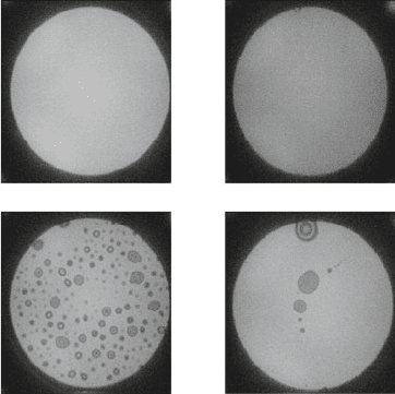
Fig. 11.11 IR images of
direct-bonded silicon wafers,
annealed at different
temperatures. (a) Room
temperature bond without
annealing; (b) bonded silicon
waver pair after thermal
treatment at 950
◦
Cfor7h;
(c) 235
◦
C anneal for 5 h; (d)
400
◦
C for 14 h. These
experiments were done in the
Stanford Nanofabrication
Facility, Stanford University,
Stanford, CA

838 S.J. Cunningham a nd M. Kupnik
separated,
5
cleaned, surface activated, and aligned again for a second trial. However,
there are some exceptions to mention. This is not the case when systems are used
that perform a heating t reatment already in the bonding tool, which makes the bond
irreversible. In addition, with the advent of the latest bonding tools featuring special
surface activation techniques (ion irradiation or in situ radical surface activation),
the full bond strength (covalent bonds) can be achieved even without such heat
treatment.
11.2.4.5 Thermal Treatment to Increase the Bond Strength
After the IR inspection there are several choices of how to proceed (Fig. 11.6). First,
depending on the initial activation method used, full bond strength might already
have been achieved, that is, covalent bonds without any or only low heat treatment
(<500
◦
C). The case of no heat treatment is still more exception than rule, but it
is heavily researched at the moment and the first commercial tools with special
surface activation modules are available. Such activations can be based on chemicals
(Ziptronix technology [23, 24]) or other techniques (ion irradiation developed by
Mitsubishi Heavy Industries LTD, in situ radical activation developed by Applied
Microengineering Ltd [25–27]).
However, most likely a heat treatment will be required after the room temperature
bond to increase the bond strength suitable for MEMS device fabrication. There are
basically two temperature ranges of interest. The annealing can be done at temper-
atures larger or lower than ∼500
◦
C, which reflects a very loose classification into
high and low temperature direct bonding. Another important classification is related
to the application of technology, that is, the limits of 400–450
◦
C (maximum tem-
perature a CMOS wafer can handle) and 800
◦
C (maximum temperature for wafers
with diffusion layers); see, for example, [28].
The heat treatment step (annealing step) is the reason why instead of direct wafer
bonding the term fusion bonding is often used. Because the bond strength (energy
of adhesion) is tremendously increased during the heat treatment (∼one order of
magnitude), the wafers “fuse” together. The mechanism when heat is applied is t o
transform the weak interatomic bonds, present after performing the room tempera-
ture bond, into strong covalent bonds. A regular oxidation furnace can be used for
high temperatures up to 1200
◦
C.
Even though the goal of the heat treatment step is the same for hydrophilic- and
hydrophobic-activated wafer surfaces, there are several differences to consider. As
shown by Tong and Gösele [6], with a heating treatment of >500–600
◦
C, the same
surface energies can be achieved for the bond, but the hydrophilic-activated wafers
already reach higher surface energies at lower annealing temperatures (200
◦
C). Note
that the given numbers in this section are for bonding in air. In general, vacuum
allows achieving higher surface energies at even lower heat treatment temperatures.
5
The thin tip of a plastic tweezers or a simple razor blade can be used to gently separate the two
wafers at the outermost edge first.
11 Wafer Bonding 839
In the rest of this section we discuss the two most studied cases, that is, heat
treatment of hydrophilic and hydrophobic silicon wafers.
Heat Treatment of Hydrophilic Silicon Wafers
The bond at room temperature for the hydrophilic wafers is formed by hydrogen
bonds between chemisorbed water molecules on both wafer surfaces. At elevated
temperatures (>110
◦
C[10]) the desorption of water molecules sets in and the water
molecules are driven away from the bonding interface. This happens either along
the bonding interface to the outside or through the native oxide to the bulk sili-
con, where t he water molecules react with the silicon to form silicon dioxide and
hydrogen. Thus, the heat treatment ensures that as soon as the water molecules have
left the bonding interface, the opposing silanol groups can come close enough and
start forming covalent Si–O–Si bonds (siloxane bonds) [8].Theformationofcova-
lent bonds translates to increased fracture surface energies (∼1.2 J m
−2
), which are
lower than the cohesive strength of silicon (∼2.5 J m
−2
, see, e.g., [29]. Only when
heat treatment temperatures of around 700–800
◦
C, or even higher, are used can the
cohesive strength of silicon be reached. Plößl and Kräuter [8] attribute this partially
to the formation of microgaps, which can only be closed when the native oxide gets
viscous enough for better compliance.
For the case that one of the two wafers has a thicker oxide film and the other
one only native oxide the situation is similar. However, this case is classified by [8]
as being ideal, that is, better compared to direct bonding two wafers with native
oxide only. This is because the native oxide from the first wafer allows the diffu-
sion of water molecules out of the interface and the thick oxide film from the other
wafer can absorb the hydrogen molecules, which reduces the formation of interface
bubbles (thermal induced voids) when moderate heating treatment temperatures are
used.
For illustration of this effect we conducted the experiment shown in Fig. 11.11.
Hydrophilic-activated silicon wafers (4 pairs) have been direct bonded and then
inspected under IR. For all four pairs a void-free room temperature bond was
achieved, as shown for the first sample, which was not annealed at all (Fig. 11.11a).
The bonds were performed with the hand bonding tool shown in Fig. 11.8.The
second sample (Fig. 11.11b), was annealed for 9 h at 950
◦
C. This temperature was
high enough so that after the heat treatment no voids were visible under IR. The
third sample, however (Fig. 11.11a), was annealed at a very moderate temperature
of only 235
◦
C for 5 h. A large number of thermal induced voids are visible after
that. For the fourth sample (Fig. 11.11d) which was annealed at 400
◦
C for 14 h, the
number of visible thermal induced voids is significantly reduced, albeit some larger
voids remained (Newton’s rings are clearly visible).
We also performed the same experiment for the case where one of each wafer
pair has a thicker oxide film, 1 μm to be specific. For the exact same three heat
treatment conditions as described before no thermal induced voids occurred.
Furthermore, such observations also provide understanding of why bonding two
oxidized silicon wafers is more difficult, in particular when the heat treatment is
840 S.J. Cunningham a nd M. Kupnik
performed at moderate temperature levels (∼500
◦
C). The thick oxide layers on both
sides make it difficult for the water molecules to diffuse through to the silicon to
react; that is, the water molecules remain and gather together to form microcavities.
In addition to the previously mentioned weak points in terms of liquid HF or HF
vapor of such an oxide to oxide bond, this is another reason why direct oxide–oxide
bonding should be avoided.
Heat Treatment of Hydrophobic Silicon Wafers
The main difference from the previous case is that the dangling bonds of the silicon
are terminated mostly by hydrogen atoms before the bond. As mentioned earlier,
these bonds are weaker than the OH groups of a hydrophilic silicon wafer. In addi-
tion, a higher heat treatment is required to increase the fracture surface strength.
As [8] outlines, a significant increase occurs at ∼400
◦
C and the cohesive strength
of silicon can be reached at 700
◦
C, which is lower than for the hydrophilic silicon
wafers (∼900
◦
C). The mechanism is similar; that is, the goal again is to transform
the weak hydrogen bonds into strong covalent silicon bonds by driving out of the
hydrogen atoms in the interface.
11.2.4.6 Remaining Fabrication Process for MEMS Device
After the heat treatment, the remaining steps required for the MEMS device fabrica-
tion can be done. Note that for these steps the choice of direct wafer bonding offers
two main advantages. First, there are no limitations in terms of temperature lim-
its because the direct wafer bond is high-temperature stable. Second, direct wafer
bonding does not add any additional materials to the wafers, such as required for
bonding with intermediate layers. As a result, the cleanliness level of the wafer does
not get degraded and diffusion clean equipment can be used after the bonding step
as well.
11.2.5 Anodic Bonding
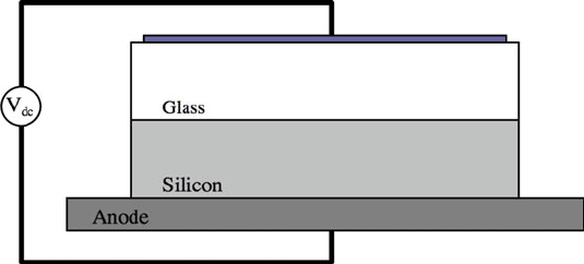
The anodic bond process has been described beginning with [30]. An electrochemi-
cal process [31, 32], it is driven by elevating the temperature of the glass–silicon
wafer pair and applying an electric potential across the wafer pair as shown in
Fig. 11.12. The silicon and glass wafers are aligned and placed together on a hot
plate with the silicon against the hot plate. The potential is applied after the tem-
perature of the wafers is raised by the hot plate and allowed to reach equilibrium.
The electric potential is applied, often times in small increments relative to the total
voltage across a small region adjacent to the silicon anode, which has been depleted
of sodium ions. The electric fields are highest in this thin depletion zone. These
high electric fields are the drivers of the oxygen anions, which are transported to the
anode interfacial surface and form an oxide with the anode atoms.
11 Wafer Bonding 841
Fig. 11.12 Basis anodic bonding process
The most common implementation of the anodic bonding process uses a silicon
substrate and a Pyrex substrate. The two materials have fulfilled the roles of both lid
and substrate, but a common scenario is an insulating Pyrex interconnect substrate
to which is bonded a silicon MEMS device and subsequently a silicon lid. The two
common process parameters are substrate temperature (180–500
◦
C) and applied
voltage (200–1000 V). The bonding process has been demonstrated with vacuum
or inert atmospheres, such as dry nitrogen, argon, neon. The atmosphere that is
being encapsulated is driven by the product requirements such as high mechanical
Q for resonators or damped frequency response for mechanical filters or high-g
products.
As shown in Fig. 11.12, the silicon and glass wafers are aligned and maintained in
intimate contact with the silicon wafer on the hot chuck of a wafer bonder. Usually,
the backside of the glass wafer is metallized for electrical contact, in which the
silicon substrate is the anode and the glass metallization is the cathode as shown. The
resultant applied electric field drive Na (or Li) ions from the glass silicon interface.
The disassociated oxygen ions react with the silicon to form an irreversible silicon–
oxide bond. The primary variables in this process are time, temperature, and voltage.
Because of the strong electrostatic pressure [33] that is developed this process is
more tolerant of surface topography or defects. During this process, the oxygen
may not be completely consumed by the silicon in the MEMS cavity. The resulting
partial pressure of oxygen will be detrimental to the vacuum level or mechanical Q
of the MEMS device. In this case, an oxygen getter will be needed to maintain the
low vacuum levels. The partial pressure of oxygen will change the viscosity of the
encapsulated gas and will need to be included in the estimate gas damping or again
eliminated through specific oxygen getters.
One aspect of this process that requires consideration is the concept that wafers
of two different materials are being bonded together at an elevated temperature.
Because the coefficients of thermal expansion for the two wafers are different,
wafer bow and interfacial stress will develop that can lead to premature failure.
The CTE for silicon and glass will vary with temperature so an optimal operating
point may be found that will minimize the stress but it may not optimize the bond
strength.
842 S.J. Cunningham a nd M. Kupnik
Depending on the process parameters, it was mentioned that the elevated temper-
atures that might be associated with the anodic bonding process could be detrimental
to integrated CMOS circuits or the MEMS materials themselves. The effect of the
anodic bonding process on integrated CMOS electronics has been studied using the
MOS capacitors. The parameters studied include N
m
, the measured concentration
of mobile ions; N
eff
,
, the measured effective oxide charge; and D
it
, the measured
density of interface traps. The effect on these parameters was examined for MOS
capacitors inside and outside the bond cavity.
N
m
, N
eff
, and D
it
all increased with anodic bonding and their increase was greater
for devices outside the cavity. The increase was least when the gap was large
between the gate electrode and the glass wafer (<10–200 μm). A silicon nitride
passivation layer over the gate electrodes reduced N
m
. The increased N
m
caused
and increased N
eff
and D
it
, for the capacitors outside the bond cavity. The increased
N
eff
and D
it
inside the cavity was caused by negative bias-temperature instability
(NBTI), which is caused by a combination of high temperature and high electric
field across the oxide. A likely reaction is for hydrogenous species A (H
2
O) react-
ing with Si–H defects to form a positive oxide charge (AH
+
) and an interface trap
(Si·)(≡ Si −H +A + p
+
↔≡Si ·+AH
+
).
The anodic bonding process described above has been used to bond wafers for the
formation of silicon microstructures such as pressure sensors, accelerometers, and
gyros. In addition, anodic bonding has been used to fabricate a wafer-level encapsu-
lation of a microstructure. A production process is described for the fabrication of
a MEMS accelerometer for automotive airbag deployment. The fabrication process
used anodic bonding to bond a silicon micromachined sensing element to a Pyrex
substrate with fixed capacitor plates. In addition, the process anodic bonded a second
patterned wafer to the same Pyrex substrate. The second silicon wafer encapsulated
the sensing element and provided a hermetic environment of a dry inert gas (i.e.,
nitrogen, neon, argon).
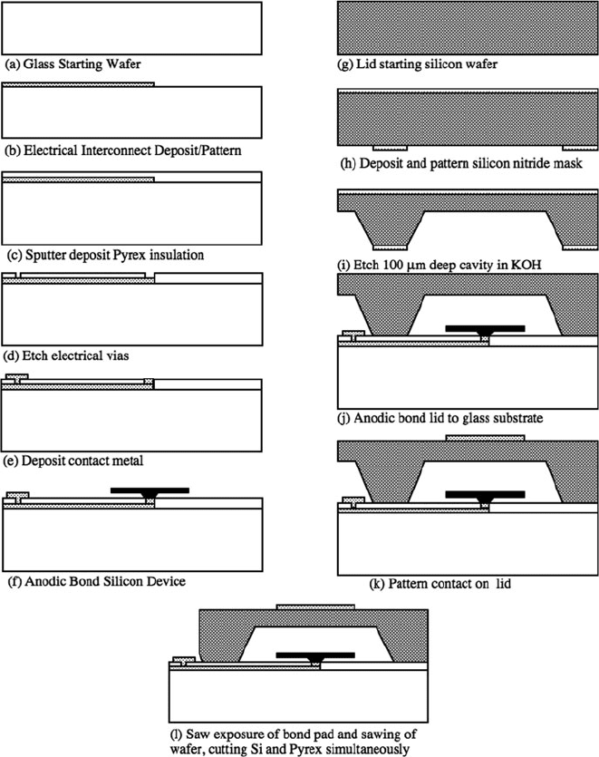
The Ford Microelectronics (FMI) waferlevel encapsulation process [34–36]isa
classic example of lateral electrical feedthroughs. Although it is not an RF device,
some of the same techniques do apply to the RF device. The goals of this process
were to provide a wafer-level, hermetic encapsulation of a silicon accelerometer
(and other products that might be developed using the same process). This elimi-
nated the coat–saw–strip process for sawing an unencapsulated device. It provided
the technology needed to put the MEMS device into a low-cost plastic package and
that was robust to the plastic packaging process. It provided an inert environment
(dry nitrogen, neon) that could be maintained for 15 years. With reference to RF
applications of this encapsulation process, the electrical feedthroughs are fabricated
on as an insulating s ubstrate (Pyrex) that will include a thin insulator (sputtered
Pyrex) between the interconnect and a silicon lid. The design of this feedthrough
performance could address the silicon resistivity, the transmission line width, and
the thickness of the sputtered Pyrex.
On the 7740 Pyrex substrate, the DC interconnects were patterned by liftoff
and deposited by evaporation of a metal stack comprised of Cr/Au/Pt/Au/Cr
(1500 Å) (Fig. 11.13a). This thickness is acceptable for DC interconnection of the
11 Wafer Bonding 843
Fig. 11.13 Accelerometer wafer-level encapsulation process
electrostatic MEMS device, but the access resistance would be limiting on the RF
performance. In the next steps, Pyrex is sputtered (1.5 μm) over the interconnects
to provide a planarized bonding interface (Fig. 11.13b). It was found for these metal
and Pyrex film thicknesses that the surface was adequately planarized to form a her-
metic anodic bond. For thicker metal films necessary for RF performance (0.5–1 μm
or thicker), the sputtered Pyrex layer would need to be thicker and a CMP process
