Ghodssi R., Lin P., MEMS Materials and Processes Handbook
Подождите немного. Документ загружается.

324 R.G. Polcawich and J.S. Pulskamp
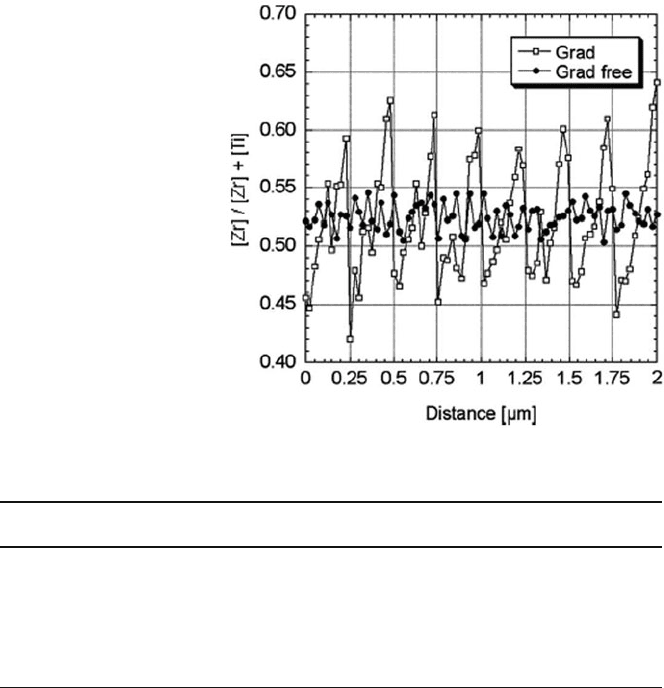
Fig. 5.50 Zr content in two
different PZT (53/47) films,
one with a standard 2-MOE
process using a crystallization
anneal every four layers and
the other using an optimized
process to reduce the Zr/Ti
gradient in the film [149]
(Reprinted with permission.
Copyright 2007 American
Institute of Physics)
Table 5.10 Material properties as a function of deposition method
Technique
Stoichiometry
(Zr/Ti)
P
r
(μC/cm
2
) E
c
(kV/cm)
e
31,f
(C/m
2
)
d
33
(pC/N) ε
33
tan δ References
MOCVD 35/65 43 130 [143]
30/70 22 65 [144]
Sputter–RF
magnetron
50/50 37.4 79 100 800–1000 0.02 [140, 166]
Inverted mixing
order (IMO)
53/47 26.2 43.3 [160]
2-MOE 53/47 –12.0 85 1180 0.029 [163]
–17.7 1650 0.023 [149]
For comparison, a list of the material properties achieved for each deposition
method has been compiled in Table 5.10. Note, that quite often, the ferroelectric
property, namely the remnant polarization, is similar for the different techniques.
However, the piezoelectric coefficients tend to be higher in the highly textured,
gradient controlled CSD techniques.
5.3.2 Patterning Techniques
Patterning PZT thin films along with many other ferroelectrics remains one of the
more challenging aspects of incorporating these compounds with MEMS. Not only
are these compounds rather difficult to etch and pattern but contamination from the

5 Additive Processes for Piezoelectric Materials 325
heavy metal elements, especially lead, poses additional problems for most clean-
rooms. Specific to PZT, regardless of the Zr/Ti ratio, this material can be etched with
all of the common etching techniques including wet processing as well as physical
and chemical etching as indicated in Table 5.11.
Table 5.11 Etch parameters for PZT thin films
Etching
parameter ECR/RIE ICP ICP Wet Ar ion mill
RF power (W) 10–200 400–800 500–800 150
Bias (V or W) 100–1000 V 100–400 V 200–350 V 36 V
Pressure (Pa or
mT)
5e
–4
to 1 Pa 1–10 mT 0.1–2.0 Pa 0.7 mT
Gas(es) CCl
4
,CF
4
,Ar Cl
2
/C
2
F
6
/Ar BCl
3
:Ar
Cl
2
:Ar
BOE:2HCl:
4NH
4
Cl:
4H
2
O
+ 2HNO
3
:H
2
O
Ar
Etch rate
(nm/min)
20–95 100–180 63–193 960 25
Resist selectivity
(PR/PZT)
3:1–13:1 1.5–3:1 3–6:1 1.5:1 1:1
References [172][174][175][169][182]
Wet etching techniques remain one of the easiest solutions to patterning PZT
especially when selectively stopping the etch on a platinum electrode. However,
this technique is limited to larger areas (several microns to tens of microns) because
most etch chemistries are highly isotropic or can even have faster lateral etch rates.
Typical chemistries involve mixtures of hydrochloric (HCl) and hydrofluoric (HF)
acids resulting in combinations of fluorine and chlorine containing by-products
[167–169]. One of the most common chemistries with relatively high etch rate and
excellent selectivity to platinum is a mixture of deionized H
2
O:HCl:HF (2:1:0.05).
The HCl acid is used to remove lead and titanium whereas the HF is used to remove
titanium and zirconium. One problem that can occur with this etch combination
occurs in films with excess lead where a white powdery lead residue remains on the
wafer surface [168]. This lead-rich residue can be removed by adding small amounts
of ammonium chloride and/or nitric acid to the solution [168]. Note that this etchant
has a lateral etch rate nearly two to three times that of the film thickness.
Chemical and physical etching via reactive ion etching (RIE) and ion-milling
can provide the necessary dimensional control necessary for creating MEMS and
NEMS structures. Similar to the wet etch chemistry, reactive ion etch techniques
utilize combinations of fluorine and chlorine containing compounds (such as CF
4
and CCl
4
)[153, 170–172]. A major challenge with a purely chemically based RIE is
the extremely low volatility of the Zr and Ti by-products, namely ZrF
4
,ZrCl
4
,TiF
4
,
326 R.G. Polcawich and J.S. Pulskamp
and TiCl
4
. To counter, the most successful etching techniques use combinations of
RF bias power in excess of 50 W, low pressures (<0.1 Pa), and elevated temperature.
One technique to etch the PZT uses an electron cyclotron resonance/radio frequency
(ECR/RF) reactor with 40% CCl
4
, 40% CF
4
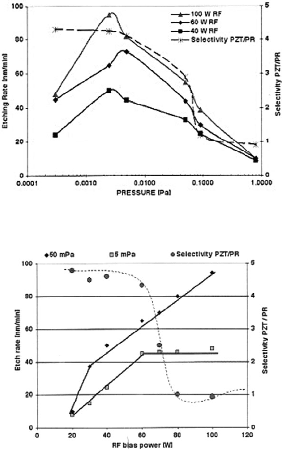
, and 20% Ar gases [153]. As shown in
Fig. 5.51, this technique can achieve etching rates approaching 100 nm/min using
100 W
RF
operating at a pressure of 1 mPa. Another chemistry for RIE is outlined
by the ferroelectric random access memory community using inductively coupled
plasma (ICP) RIE reactors with 70% BCl
3
and 30% Ar gas [173–175]. In addition
to etching PZT layers, RIE can be used to etch the electrode layers such as Pt,
RuO
2
, and IrO
2
. In general, the leading etch chemistries use chlorine containing
gases such as Cl
2
, CCl
4
, and BCl
3
with the etch mechanism being mostly physical
in nature [153, 175–177].
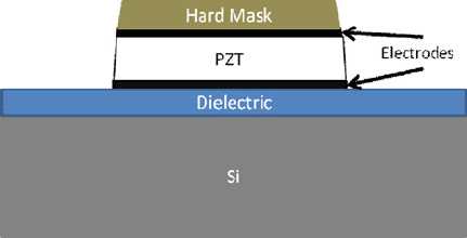
Fig. 5.51 Cross-section
image/schematic of an
FRAM capacitor
(Ir/IrOx/PZT/IrOx/Ir)
patterned using a single-layer
hard etch mask of TiAlN
The two biggest challenges with a chemical RIE approach to patterning PZT
are controlling re-deposition of the nonvolatile etch by-products and achieving the
necessary resist selectivity. Processing at higher temperatures and using low pres-
sures combined with high-throughput vacuum pumps increases the percentage of the
by-products remaining in the gaseous phase. However, increasing the temperature
causes severe resist degradation or even carbonization of the photoresist. As a result
a hard mask needs to be employed. Further evidence of this is shown in Figs. 5.51
and 5.52 where resist selectivity dramatically decreases with increases in process-
ing pressure or incident ion energy or RF bias. Resist degradation is yet another
challenge with RIE etches of PZT. To preserve the resist integrity, any masking
must be done with either hard-cured photoresist or hard masks to avoid degrada-
tion in soft-cured photoresist. Early work on hard masks included TiO
2
coatings
with the FRAM community moving toward TiN or TiAlN coatings [178, 179]. The
use of hard coatings enables a single mask layer etching process to etch the entire
capacitor,electrode/PZT/electrode (see Fig. 5.53). The same process can be used for
MEMS actuators. However, care must be taken to account for the elevated voltages
that the actuators require compared to that of FRAM. The gap separation between
the t wo electrode layers is defined by the PZT thickness. Because this separation
can be in the range of 0.25–2 μm, breakdown across the air gap becomes a concern
during device operation. For example, actuators comprised of a 0.5 μmPZTfilm
5 Additive Processes for Piezoelectric Materials 327
Fig. 5.52 Etching characteristics of PZT thin films as a function of RF bias power using an
electron cyclotron resonance/radio frequency (ECR/RF) reactor [180] (Reprinted with permission.
Copyright 2000 Taylor & Francis)
Fig. 5.53 Etching characteristics of PZT thin films as a function of processing pressure using an
electron cyclotron resonance/radio frequency (ECR/RF) reactor [180] (Reprinted with permission.
Copyright 2000 Taylor & Francis)
with Pt electrodes fabricated with a single etch process have breakdown voltages
on the order of 10 V (∼200 kV/cm). In contrast, employing a multiple step etching
process to define the actuator increases the breakdown voltage for a 0.5 μm thick

328 R.G. Polcawich and J.S. Pulskamp
Fig. 5.54 Schematic cross
section of PZT stack
actuators patterned using (a)
a single etch process and (b)a
multiple step etch process
PZT actuators to approximately 100 V (∼2000 kV/cm). This effect is primarily due
to the fact that the PZT overlap required for the multistep etch/masking process
increases the distance between the top and bottom electrodes (see Fig. 5.54).
The final method of patterning PZT thin films is through a physical etch using
Argon ion-milling. Although this technique does not provide any significant selec-
tivity to photoresist, PZT, or the electrode layers, it has several key advantages
including the ability to etch the entire metal/PZT/metal stack and variable control
of the angle of incidence [181]. For hard-to-etch compounds, especially materials
with low volatility such as PZT and Pt, the accelerated Ar ions can be used to break
the atomic bonds, and the variable angle control is used to push free atoms away
from the wafer surface. Furthermore, the angle of incidence can be altered during
the final stages of the etching to remove any re-deposited materials. Similar to the
chemical-based RIE procedures, the masking material for the ion-mill must either be
hardened photoresist or a hard mask as ion-damage and re-deposited heavy metal
ions prevent clean removal of a soft photoresist. Although the ion-mill generally
has poor selectivity and a difficulty to accurately endpoint on the desired layer, an
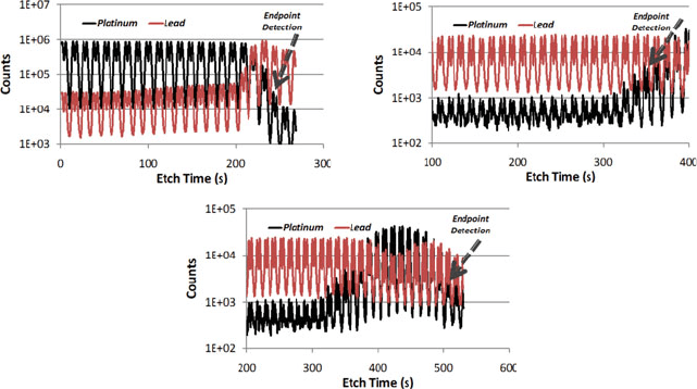
ion-mill reactor can be configured with a secondary ion mass spectrometer (SIMS)
endpoint detection system. The SIMS system analyzes the etched material as it is
removed from the wafer surface and yields an accurate depiction of the depth of the
current etch. An example of the endpoint detection is illustrated in Fig. 5.55 for a
sample etching the top Pt electrode stopping on the PZT and for a sample etching
the PZT and stopping on the bottom Pt electrode.
5.3.3 Device Design Concerns
Designing piezoelectric-based MEMS with PZT poses several challenges in the
realm of device processing and electromechanical design. The processing chal-
lenges include thermal processing budget, residual stress gradients, processing
induced damage, and ferroelectric domain poling. Achieving high-quality PZT
thin films for piezoelectric actuators nominally requires annealing conditions with
temperatures in the range of 600–750
◦
C as previously discussed. As a result, it
is imperative to thermally stabilize the underlying materials not only to ensure
their compatibility with the processing temperature but also to minimize changes
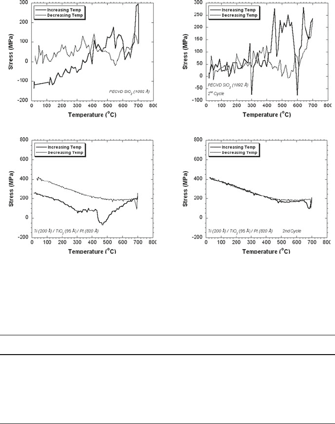
in residual stress. As an example, the changes in residual stress with plasma-
enhanced chemical vapor deposited (PECVD) silicon dioxide (SiO
2
) and a sputtered
Ti/TiO
2
/Pt thin film on a PECVD SiO
2
are illustrated in Fig. 5.56. The first plots
5 Additive Processes for Piezoelectric Materials 329
(c)
(a) (b)
Fig. 5.55 Examples of using SIMS endpoint detection in conjunction with ion-milling of (a)Pt
etching and stopping on a PZT thin film using the falling edge of Pt, (b) etching PZT and stopping
on a Pt thin film using the rising edge of Pt, and (c) etching PZT and Ti/Pt stopping on the under-
lying SiO
2
using the falling edge of Pt. Note: the double peaks in the SIMS signal are the result
from monitoring two substrates that are rotated under the beam during the etching process
compare the initial and second anneal of a PECVD SiO
2
and the next two plots
compare the initial and second anneal of a Ti/TiO
2
/Pt thin film. As shown, signif-
icant changes in the room temperature film stress result from the initial thermal
processing whereas the stress remains stable in subsequent anneals [182].
Two important characteristics that result from the use of multilayer composite
structures for a piezoelectric thin film actuator or sensor are residual stress gradi-
ents and thermally induced deformations. Each film within the composite typically
has different magnitude stress values resulting primarily from the coefficient of ther-
mal expansion mismatch with the substrate (in most cases, silicon). Table 5.12 is an
example illustrating the ranges of film stress in a six-layer composite consisting of
combinations of silicon dioxide, silicon nitride, a titanium/platinum bi-layer, PZT,
and Pt. The stress gradient requires careful consideration in the design of piezo-
electric devices. For devices requiring flat stable structures, improper design can
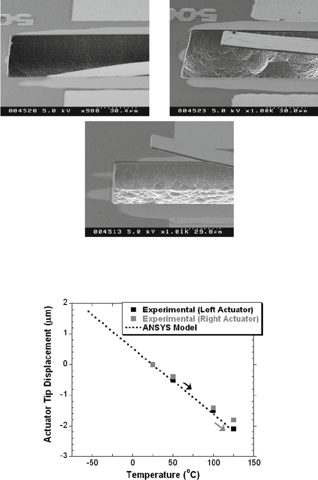
lead to structures with drastic undesired deformations (see Fig. 5.57). Similarly, the
stress gradient can be controlled to enable device specific attributes such as restor-
ing force. Proper stress gradient control created repeatable negative curvature in a
PZT actuator used to create piezoelectric switches [29, 182].
The second aspect of the multilayer stack is thermally induced deformations
resulting from differences in the coefficient of thermal expansion between the layers
in the composite. Using the same materials listed in Table 5.12, an example of the
thermal deformations is illustrated in Fig. 5.58. As shown, deformations as large as
4 μm are observed from –50 to 100
◦
C for an approximately 150 μm long composite
330 R.G. Polcawich and J.S. Pulskamp
(a) (b)
(c) (d)
Fig. 5.56 Change in residual stress as a function of temperature for the initial and second thermal
anneal for (a)and(b)PECVDSiO
2
and (c)and(d)Ti/TiO
2
/Pt on a thin layer of SiO
2
Table 5.12 Average residual stress measured on each of the thin films used i n the composite
actuator for a PZT switch [29]
Film Nominal thickness (Å) Stress (MPa) Std Dev (σ)
SiO
2
1000 33.1 10
Si
3
N
4
500 1100 200
SiO
2
3500 33.1 10
Ti/TiO
2
/Pt/TiO
2
160/90/1640/10 323 83.3
PZT 5000 175 7.26
Pt 1050 76.3 16.5
Reprinted with permission. Copyright 2007 IEEE
actuator comprised of a 0.5 μm elastic layer (SiO
2
/Si
3
N
4
/SiO
2
) and 0.5 μmPZT
(52/48) thin film using Ti/Pt and Pt electrode layers.
Another area of concern for PZT-based MEMS devices is degradation in the
material properties during device fabrication. The research on ferroelectric random
access memory has advanced the understanding of the leading degradation mecha-
nisms including ion damage, H
2
damage, and surface contaminants [181, 183, 184].
In many instances, the manifestation of damage in the PZT can be observed through
5 Additive Processes for Piezoelectric Materials 331
(a) (b)
(c)
Fig. 5.57 SEM images illustrating a wide range of curvature achievable in a multilayer PZT thin
film composite consisting of the layers outlined in Table 5.12. The change in curvature from (a)to
(c) is achieved by simply moving the location of the high-tensile stress silicon nitride layer from
near the bottom of the composite toward the center
Fig. 5.58 Thermally induced deformations (experimental and finite element predictions using
ANSYS) for a multilayer PZT thin film actuator consisting of SiO
2
/Si
3
N
4
/SiO
2
/Ti/Pt/PZT/Pt [29]
(Reprinted with permission. Copyright 2007 IEEE)
332 R.G. Polcawich and J.S. Pulskamp
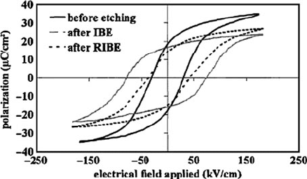
Fig. 5.59 Change in the polarization electric field hysteresis loop observed for virgin (before
etching) PZT thin films, for a PZT film exposed to ion-milling (after IBE), and for a PZT film
exposed to a reactive ion etch (after RIBE). For both etched samples, the testing was done after
depositing and annealing a top Pt electrode layer on the etched surface [183] (Reprinted with
permission. Copyright 2005 American Institute of Physics)
characterization of the ferroelectric and dielectric properties. In cases where the
PZT surface is exposed to etch conditions and then electroded, reductions in the
remnant polarization, increases in the coercive field, and decreases in the dielectric
constant are observed resulting from the creation of a damaged surface layer lying
beneath the top electrode (see Fig. 5.59)[181, 183]. The presence of the damaged
surface layer is severely detrimental to the performance of the PZT and consequently
the preferred process deposits and patterns the top electrode onto the as-deposited,
pristine surface of the PZT film.
For piezoelectric devices patterned after the top electrode has been deposited,
degradation remains a potential problem. The PZT sidewalls are damaged during
the patterning process and can introduce defects into the material. More important,
exposure to H
2
through contact with the hydrocarbons in photoresist and forming
gas anneals introduces protons in the PZT via diffusion, adversely affecting the
ferroelectric and dielectric properties through domain pinning.
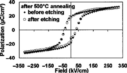
Regardless of the damage created by processing, in most instances the ferroelec-
tric and dielectric properties can be recovered using a thermal anneal. To approach
full recovery, the anneal must be done above the Curie temperature of the ferroelec-
tric. An example of how effective the recovery anneal can be is shown in Fig. 5.60.
In this example, the material properties are recovered to the initial conditions using
a 500
◦
C anneal.
Another key aspect with PZT devices is the aligning of the ferroelectric domains
or poling. Unlike the pure polar materials discussed previously (i.e., AlN and ZnO),
the polarization in ferroelectric materials can be configured in a multitude of orien-
tations. In order to optimize the piezoelectric coefficient of the PZT, the ferroelectric
domains need to be aligned in a single preferred direction. For an actuator in a par-
allel plate configuration (d
31
mode), the poling direction is along the film thickness.
The most direct method of poling is the application of an electric field nominally
5 Additive Processes for Piezoelectric Materials 333
Fig. 5.60 Illustration of how high-temperature annealing can be used to recover the ferroelectric
properties of PZT thin films after damage induced by the patterning process [181] (Reprinted with
permission. Copyright 2002 American Institute of Physics)
3–4 times the coercive field for 10–15 min (i.e., 10–15 V f or a 0.5 μm thick film).
Additional techniques can be employed to further increase the piezoelectric coeffi-
cient including thermal poling and exposure to ultraviolet radiation consisting of a
wavelength smaller than the absorption band gap of the material (i.e., approximately
365 nm for PZT). With thermal poling, the electric field for poling is applied and
the PZT is held at temperatures approaching half of the Curie temperature or higher,
nominally 125–150
◦
C.
5.3.4 Device Examples
This section is intended to give the reader an understanding of the full capabilities
of using PZT thin films for piezoelectric MEMS and how to specifically implement
them in devices. Each of the main research areas of PiezoMEMS based on PZT is
covered with detailed descriptions of several highlighted successful device demon-
strations. In the last part of this section, a full case is undertaken for a piezoelectric
RF MEMS microswitch.
In the area of sensors, PZT-based acoustic detection, infrared detectors, and
energy harvesting have led the research community. As infrared detectors are based
on the pyroelectric effect, or the change in polarization with temperature, and
not piezoelectricity, the readers are directed to the research in [3, 185–187]for
more detail. Acoustic detectors based on PZT have been demonstrated across a
wide spectrum of frequencies. At low or audible frequencies, PZT thin-film-based
microphones have been demonstrated with modest performance characteristics.
Another application for PZT-based acoustic sensors is nondestructive, real-time
imaging using ultrasound array transducers. Thin- and thick-film PZT can be assem-
bled to form arrays of piezoelectric micromachined ultrasonic transducers (pMUTs)
[188–193]. Compared with conventional ceramic-based ultrasound systems, the
