Ghodssi R., Lin P., MEMS Materials and Processes Handbook
Подождите немного. Документ загружается.

304 R.G. Polcawich and J.S. Pulskamp
Table 5.4 Comparison of the surface roughness (RMS) and full width at half maximum (FWHM)
for sputtered AlN films on various substrates and thin films [97]
Substrate Si Si/Mo Si/SiO
2
Si/Si
3
N
4
Si/SiO
2
/Ti/Pt
Substrate roughness, R
rms
(Å) 0.94 5.10 0.91 1.27 3.49
AlN roughness, R
rms
(Å) 12 46.3 11.4 16.0 39.7
AlN (0002), FWHM (
◦
) 1.82 5.15 1.78 1.90 2.37
Reprinted with permission. Copyright 2003 American Vacuum Society
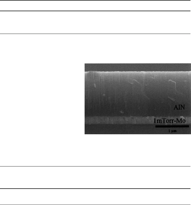
Fig. 5.28 SEM image
illustrating the columnar
growth and smooth texture of
a sputtered AlN film
deposited onto Mo on a Si
substrate [96] (Reprinted with
permission. Copyright 2003
American Vacuum Society)
Table 5.5 Influence of a Ti seed layer on the sputter deposition of both Mo and AlN films [99]
Substrate
Mo deposition
temperature
(
◦
C)
Mo
roughness,
R
rms
(Å)
Mo
FWHM (
◦
)
AlN
roughness,
R
rms
(Å) AlN FWHM (
◦
)
No seed layer 250 3.86 6.2 12.60 3.6
Ti seed (30 nm) 250 2.75 2.1 7.44 1.7
Reprinted with permission. Copyright 2004 American Vacuum Society
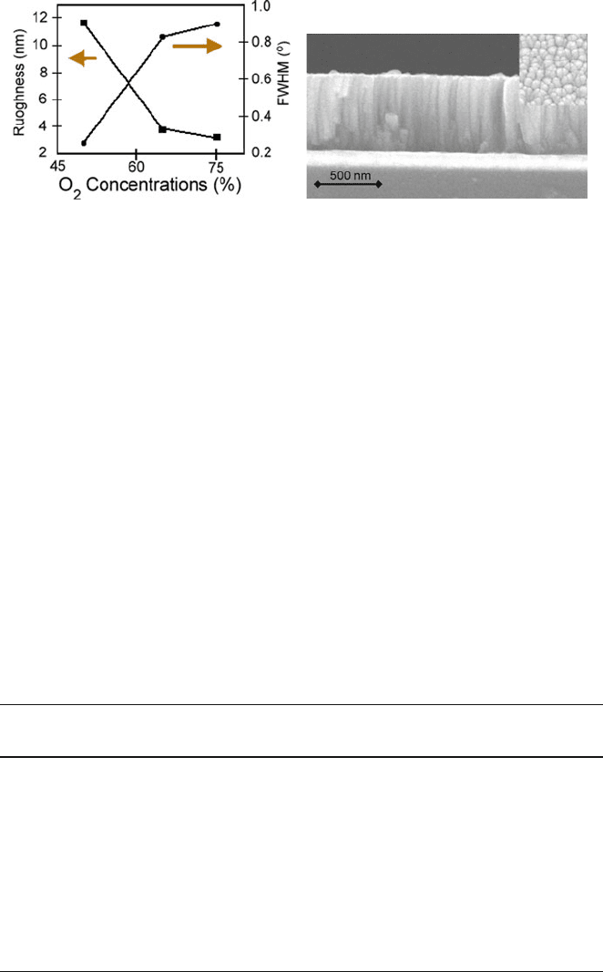
in Fig. 5.29a, increases in oxygen percentage in a Ar/O
2
mixture leads to decreases
in the surface roughness. However, the FWHM of the [0002] peak increases. One
method of achieving improvements in both the RMS roughness and FWHM is to
use a two-step deposition process [105]. In the process outlined by Lin, Chen, and
Kao [105], the initial step uses a high oxygen percentage (75%) to deposit a smooth
starting layer of ZnO. The second deposition processes s witches to a lower oxygen
percentage (50%) to increase the texture quality of the film along with maintaining
accurate stoichiometry. The resulting film exhibits a columnar growth pattern along
with an improved surface quality (see Fig. 5.29b).
5 Additive Processes for Piezoelectric Materials 305
(b)(a)
Fig. 5.29 (a) Influence of oxygen concentration on the texture and surface roughness of RF sput-
tered ZnO thin films and (b) an SEM image of a sputtered ZnO film deposited using a two-step
process [105] (Reprinted with permission. Copyright 2007 Springer Science+Business Media)
5.2.2 Patterning Techniques
In order to enable the full integration potential of AlN and ZnO, selective pattern-
ing capabilities are required including both wet chemical and dry etch processes. A
key aspect of wet chemical processes is their tendency to be very isotropic result-
ing in reasonably large lateral etch rates. However, under many circumstances, wet
etching is preferred to avoid the physical damage and generally low selectivity of
physical etch techniques. Both AlN and ZnO can be removed with wet chemical
etch processes and a list of known etchants have been assembled in Table 5.6.An
important characteristic about ZnO is that its material quality (texture, dielectric
loss, and breakdown strength) are well known to be extremely sensitive to micro-
fabrication processes [107]. As a result care must be taken not only to protect it
during the etching process but also during the remainder of the device fabrication
processes. Protection layers can include the use of silicon dioxide and silicon nitride
barrier layers to name a few.
Table 5.6 Summary of wet etching techniques for AlN and ZnO thin films
Etching
parameter AlN AlN AlN AlN ZnO ZnO
Chemical(s) AZ400K
(KOH)
KOH (10%) TMAH H
3
PO
4
(85%) HCl (0.1 M) CH
3
COOH:
H
3
PO
4
:H
2
O
(1:1:60)
Mask Apiezon
wax
Ti Cr
Temperature
(
◦
C)
85 RT–85 RT 60 RT RT
Etch rate
(nm/min)
6–1000 6–1500 22 600–3000 300–1200 ∼800
References [108, 109][109, 110][111][112, 113][107, 114,
115]
[107, 116]
306 R.G. Polcawich and J.S. Pulskamp
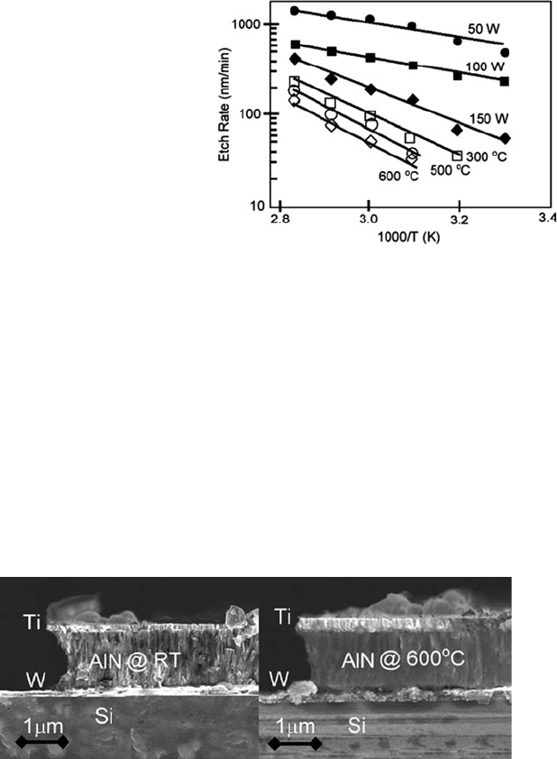
Fig. 5.30 AlN wet etch rates
in 10 wt% KOH as a function
of solution temperature,
deposition temperature, and
the deposition power of
sputtered AlN [110]
(Reprinted with permission.
Copyright 2008 Elsevier)
The ability of etching AlN has a very strong relationship to the crystalline quality
of the thin film. As discussed previously, the crystalline quality is highly dependent
on the deposition parameters. Similarly, the etching rates are linked to the deposition
conditions. The example in Fig. 5.30 illustrates the variance in etching conditions
as a function of solution temperature, RF deposition power, and substrate deposi-
tion temperature. In addition, the lateral etch rates also vary as a function of the
crystalline quality of the film (see Fig. 5.31). Another crucial point in the primary
wet etch for sputtered AlN films is KOH, the main component in some photoresist
developers [108, 109]. Therefore, special concern must be taken in the selection
of photoresists and developers used during the microfabrication process. Similar to
ZnO films, the use of barrier coatings such as silicon dioxide or silicon nitride thin
films are common.
Fig. 5.31 SEM images of sputtered AlN following a wet etch in 10 wt% KOH for films deposited
at RT and 600
◦
C[110] (Reprinted with permission. Copyright 2008 Elsevier)
Physical etching of AlN and ZnO by various etching techniques is the choice
for precision definition of MEMS devices. In general, chlorine plasmas are used for
AlN etching and fluorine plasmas are used for ZnO. A list of common physical etch
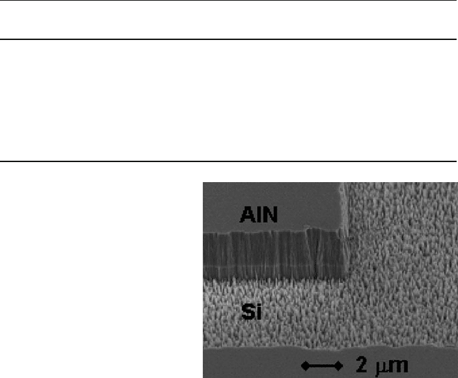
techniques for both compounds is given in Table 5.7. In contrast to wet chemical
etching, physical etching leads to nearly vertical sidewalls under the appropriate
etch conditions (see Fig. 5.32). For AlN, the use of hydrogen in the etch chemistries
5 Additive Processes for Piezoelectric Materials 307
Table 5.7 Summary of plasma etch techniques for AlN and ZnO
Etching
parameter AlN AlN AlN ZnO ZnO
System ECR ICP ICP ICP ICP
Chemical(s) Cl
2
/H
2
Cl
2
/Ar (5:1) Cl
2
or Cl
4
/H
2
C
2
F
6
C
2
H
6
/H
2
/Ar
RF power (W) 200 500 100–1500 700–1000 300
Bias (V or W) –150 V –100 to –350 V 0 to –100 V 50–200 W
Pressure (Pa) 0.13 0.26 0.26–2 0.4–2 0.26
Etch rate
(nm/min)
10–40 50–700 50–150 410 50
References [117][118, 119][120][121][122]
Fig. 5.32 SEM of an AlN
layer etched using an ICP
plasma using a Cl
2
/Ar gas
mixture
tends to lead to equal etching rates for the group III and group V components and
leads to smoother etch surfaces [117].
5.2.3 Device-Design Concerns
Designing piezoelectric MEMS with AlN or ZnO requires attention to several key
aspects that affect the overall device performance. The choice of film thickness has
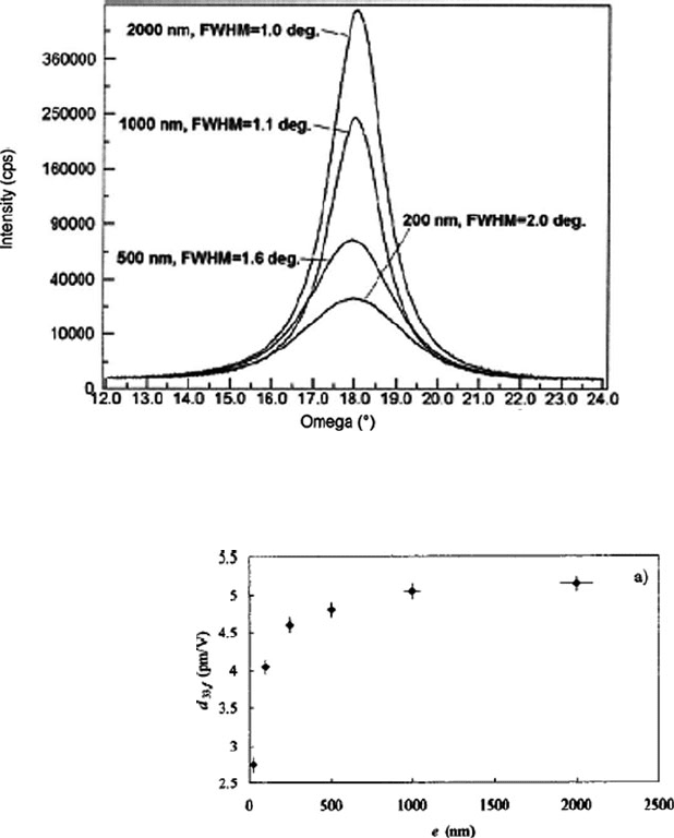
a direct impact on the crystalline texture and piezoelectric coefficient. The initial
growth starts with epitaxial matching to the substrate or electrode surface leading
to strained growth with a relatively broad FWHM. For sputtered AlN, as the film
thickness increases, the alignment of the crystals improves, reducing the FWHM to
near 1 degree and increasing d
33, f
toward 5 pm/V (see Figs. 5.33 and 5.34)[90,
123].
In most applications, parallel plate configurations (d
31
mode) are utilized requir-
ing the use of multilayer composites. As a result, control of residual stress gradients
is imperative and starts with an understanding of the residual stress in the piezoelec-
tric. Similar to the FWHM and piezoelectric coefficient, the residual stress heavily
308 R.G. Polcawich and J.S. Pulskamp
Fig. 5.33 RockingcurveFWHMand d
33, f
as a function of film thickness for sputtered AlN on
Si/SiO
2
/Ti/Pt [123] (Reprinted with permission. Copyright 2009 American Vacuum Society)
Fig. 5.34 d
33, f
as a
function of film thickness for
sputtered AlN on
Si/SiO
2
/Ti/Pt [90] (Reprinted
with permission. Copyright
2004 American Vacuum
Society)
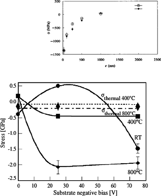
depends on the film thickness, primarily a result of high interface stresses as the
piezoelectric is strained to match the underlying layers. As shown in Fig. 5.35,the
stress of a sputtered AlN on Pt changes from compressive to tensile with increas-
ing thickness, for the deposition parameters in [90]. In addition to the stress being
dependent on the film thickness, the deposition parameters (RF or DC bias, pres-
sure, gas flow, and temperature) can greatly influence the residual stress [22, 101,
102, 104]. In many instances, the film stress can be controlled over a wide spec-
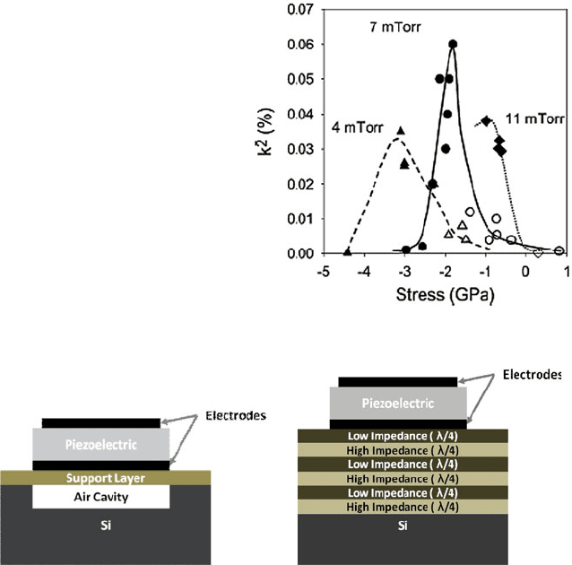
trum from compressive to tensile stress (see Fig. 5.36 ). In addition, the film stress
and the coupling factor have been shown to be interrelated creating a more chal-
lenging situation to achieve both low stress and high piezoelectric properties (see
Fig. 5.37).
5 Additive Processes for Piezoelectric Materials 309
Fig. 5.35 Residual stress as a
function of film thickness for
a sputtered AlN film on
Si/SiO
2
/Ti/Pt [90] (Reprinted
with permission. Copyright
2004 American Vacuum
Society)
Fig. 5.36 Residual stress of AlN deposited on Si as a function of substrate bias and substrate
temperature [101] (Reprinted with permission. Copyright 2006 Elsevier)
5.2.4 Device Examples
This section provides a sampling of the capabilities of polar thin films in MEMS
and how they have been implemented in devices. Examples highlighting some
recent successes are presented, followed by a full case study in AlN contour-mode
resonators and filters.
The cell phone industry has been driving RF filter innovation in recent years, pro-
viding challenging requirements for filter selectivity, power handling, temperature
insensitivity, and filter figure of merit (k
2
eff
Q)[124]. Film (or “free-standing”) bulk
310 R.G. Polcawich and J.S. Pulskamp
Fig. 5.37 The interplay
between the
electromechanical coupling
factor and residual stress at
different deposition pressures
for sputtered AlN films on Si
and Si/SiO
2
[91] (Reprinted
with permission. Copyright
2004 Elsevier)
(a) (b)
Fig. 5.38 Illustration of (a) film bulk acoustic resonator (FBAR) structure and (b) solidly mounted
resonator (SMR). B oth devices are typically realized with AlN thin films
acoustic resonator and filter technology now represents a significant commercial
success story in RF MEMS. AlN FBAR devices feature extensional thickness-mode
thin-film piezoelectric membrane resonators that are suspended above a silicon
substrate (see Fig. 5.38). In addition to the free-standing FBAR structures, the
solidly mounted resonator (SMR) device utilizes a series of acoustic impedance
mismatch layers directly below the resonator to retain acoustic energy within the
transducer.
SMR devices tend to be more robust than the FBAR but have inferior RF per-
formance due to degradation in mechanical quality factor with enhanced acoustic
energy radiation into the substrate. Both SMR and FBAR devices have a number
of advantages over competing technologies such as surface acoustic wave devices
(SAWs), including superior figure of merit, power handling, electrostatic discharge
insensitivity, and size [125, 126]. Avago Technologies, formally Agilent’s semicon-
ductor products group, has sold hundreds of millions of FBAR-based units including

5 Additive Processes for Piezoelectric Materials 311
(a) (b)
Fig. 5.39 (a) Micrograph of an example FBAR filter from Avago Technologies Inc. The active
filter area is indicated by the white rectangle [125] (Reprinted with permission. Copyright 2008
IEEE) and (b) Micrograph of singulated packaged FBAR filters from Avago [127] (Reprinted with
permission. Copyright 2002 IEEE)
filters, duplexers, and multiplexers. The Avago FBAR device (see Fig. 5.39) fab-
rication begins with etching and backfilling portions of the silicon substrate with
a sacrificial oxide [125]. Once the wafer is polished, a Mo film is deposited and
patterned as an electrode. The AlN film is then sputter-deposited and patterned
and followed by the deposition and patterning of the Mo top electrode. Following
additional processing, the structures are released with HF. The Avago devices are
hermetically sealed in a low-cost wafer-level package [127]. The patented process
bonds the FBAR s ilicon substrate with a second silicon wafer housing vias, seals,
and alignment marks. The cap wafer is subsequently thinned with conventional
wafer-thinning. DRIE is then used to open access to the FBAR contacts.
Despite the advantages and success of FBAR devices, there remains a need for
integrating small-scale and low-power multiple-frequency and multiple-standard RF
devices [128]. Cost-effectively integrating large numbers of multiple frequency fil-
ters appears difficult for FBAR devices as they rely on extensional thickness modes
to determine center frequency. In contrast, contour-mode resonators have center fre-
quencies determined by their lithographically definable lateral dimensions. Great
progress has been made during the last few years in both ZnO and AlN contour
mode resonators [129–132].
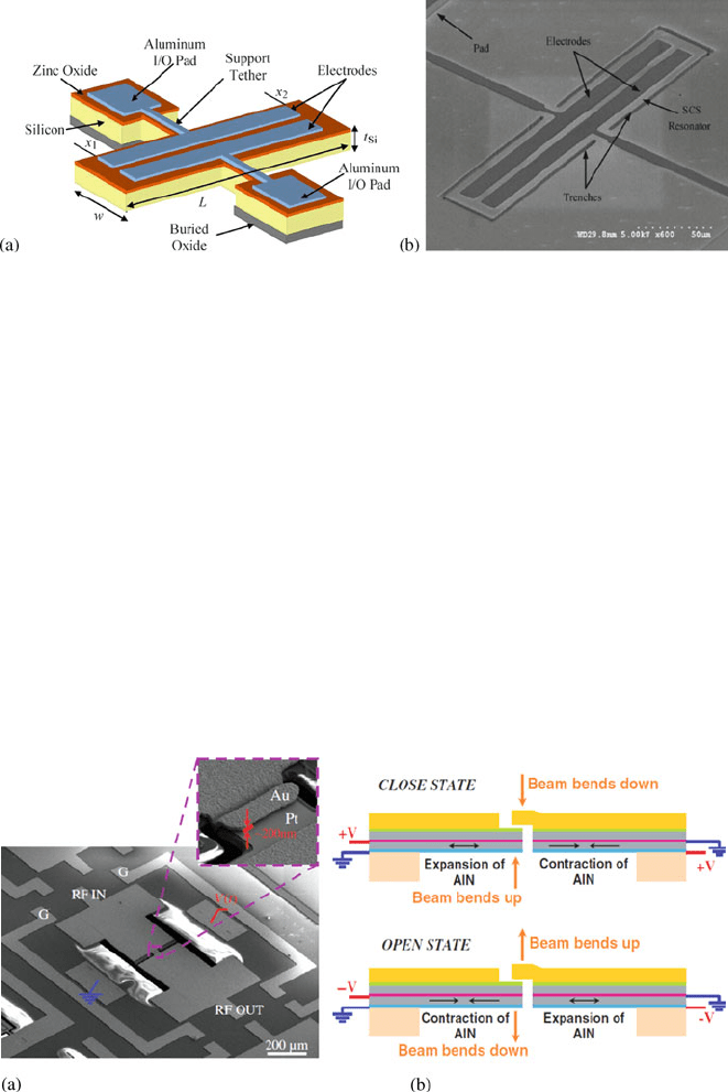
High performance extensional contour mode resonators have been demonstrated
in ZnO (see Fig. 5.40). Referring to the research in [ 129], the devices make use
of high-quality single crystal silicon as the bulk of the resonator to provide low
volumetric mechanical losses. Loaded quality factors in vacuum have been demon-
strated with values as high as 11,800 with motional resistances of 1600 . Motional
resistances as low as 600 have also been shown, however, with lower Qs. The
resonators are fabricated with a three-mask process that begins with patterning an
SOI-based single crystal silicon resonator. ZnO films are then deposited on the
Cr–Au electroded resonator structures. After an Al top electrode is deposited and
patterned, the ZnO is finally patterned to provide bottom electrode access.
A number of transduction techniques have been utilized in the actuation of
RF MEMS switches, including electrostatic, electromagnetic, thermomechanical,
312 R.G. Polcawich and J.S. Pulskamp
Fig. 5.40 (a) Illustration and (b) SEM of a ZnO on silicon lateral bulk acoustic resonator [129]
(Reprinted with permission. Copyright 2008 IEEE)
and piezoelectric. The interest in radio and cell-phone frequency compatible AlN-
based filters has motivated the development of integrated piezoelectric RF MEMS
switches. AlN piezoelectric RF MEMS switches have recently been demonstrated
with good RF performance at these frequencies of interest [133]. These devices
feature an innovative approach to address residual stress deformation, temperature
sensitivity, and the modest piezoelectric coefficients of AlN. A symmetric “dual-
beam” design features pairs of actuators t hat experience similar residual stress and
temperature-induced deformations that minimize variations in the open-state contact
gap despite the mechanical fluctuations (see Fig. 5.41). The device shows immu-
nity to residual stresses, fast switching speeds (∼2 μs), moderate actuation voltage
(∼20 V), and good low frequency isolation (>26 dB) and insertion loss (<0.7 dB) at
2 GHz. These devices have also been successfully cofabricated on the same wafer
as contour-mode AlN RF MEMS resonators. The device fabrication leverages the
process used for AlN contour-mode resonators. Once these features are defined,
Fig. 5.41 (a) SEM image of AlN RF MEMS switch with inset indicating the nanogap contact
location and (b) illustration of principle of operation of “dual-beam” architecture [133] (Reprinted
with permission. Copyright 2008 Institute of Physics)
5 Additive Processes for Piezoelectric Materials 313
including multiple AlN and Pt electrode deposition and patterning steps, an amor-
phous silicon sacrificial layer is deposited and patterned with liftoff. This is followed
by the deposition and patterning of a thick electroplated Au layer to provide RF
transmission lines and unimorph actuator features. The switch is released using a
xenon difluoride dry release to complete the process.
A number of groups are investigating mechanical logic technologies to address
the limitations imposed in CMOS by gate oxide leakage. Static power consump-
tion now rivals dynamic power consumption in CMOS and presents a significant
challenge to the continued scaling of CMOS logic devices. Motivated by low-power
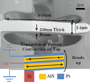
nanomechanical logic applications, AlN nanoactuators have recently been demon-
strated [134]. AlN thin films with a thickness of 100 nm were implemented in
nanoscale bimorph cantilevered actuators. Displacements of 40 nm were achieved
at 2 V in 18 μm long cantilever devices. The actuators were fabricated using a
five-mask post-CMOS compatible process similar to the process outlined for the
fabrication of the AlN RF MEMS switch discussed above. A key difference in the
process, however, is the use of a focused ion beam (FIB) tool. The nearly complete
suspended clamped–clamped AlN beam is severed at one anchor with the FIB to
create the cantilevered device seen in Fig. 5.42.
Fig. 5.42 SEM image of
AlN cantilevered bimorph
nanoactuator [134]
(Reprinted with permission.
Copyright 2008 IEEE)
5.2.5 Case Study
As discussed earlier, there is great interest in developing highly integrated multi-
ple frequency arrays of filters and resonators for RF applications. Recent progress
in both AlN contour-mode filters and RF MEMS switches suggests this technol-
ogy could become a viable commercial product [128, 132, 133, 135]. The devices
are generally near-symmetric Pt/AlN/Al composite structures with AlN thicknesses
typically in excess of a micron [131]. The contour vibrational modes are excited
