Ghodssi R., Lin P., MEMS Materials and Processes Handbook
Подождите немного. Документ загружается.

334 R.G. Polcawich and J.S. Pulskamp
pMUTs offer the potential of s maller size systems resulting from MEMS fabrica-
tion, higher frequency for improved resolution (targeting 10–100 MHz), and better
impedance matching to air and water [194]. To achieve their full potential, these
arrays require a high electromechanical coupling factor enabling a large bandwidth,
high efficiency, and minimal cross-element noise and high aspect ratio structures
[195]. Similar to the low-frequency microphones discussed previously, membrane
structures have been the typical incarnation of the pMUT. An example of such a
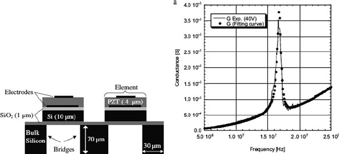
device is in Fig. 5.61 in which a 4 μm thick PZT layer was combined with a 10 μm
Si device layer to yield a transducer operating at 16.9 MHz with a quality factor Q
of 25 in air and coupling factor, k
2
of 3% [195]. One limitation with conventional
micromachining approaches is difficulty in achieving ultrahigh aspect ratios neces-
sary for l ow MHz operation. Recent work on using spray-mist deposition of PZT
solutions may be a means of achieving such technology (see [196]).
Fig. 5.61 Example of a pMUT comprised of a Si/SiO
2
/Ti/TiO
2
/PZT/Cr/Au fabricated using
Si DRIE to create t he membrane [195] (Reprinted with permission. Copyright 2007 Springer
Science+Business Media)
Actuation technology continues to be a strong area of development for piezoelec-
tric MEMS including ultrasonic motors, micromirrors, RF devices, and robotics.
Ultrasonic motors using thin-film PZT were investigated initially in the middle
1990s as possible replacements for actuators in wrist watches [197, 198]. For this
device, a piezoelectric membrane stator is combined with a set of elastic fins on a
rotor. As the resonant wave is generated within the membrane, it periodically com-
presses the elastic fins resulting in movement in the rotor as the elastic fins relax after
contacting the membrane [199]. Similar to the previously discussed membranes,
they were created using a combination of bulk and surface micromachining tech-
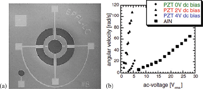
nologies. The device and data shown in Fig. 5.62 were from a membrane patterned
using a KOH etch to create the Si membrane structure. This configuration using a
1 μm PZT film was able to achieve nearly 100 rad/s at 5 V, nearly two orders of
magnitude higher velocity compared with an AlN stator of comparable frequency
anda2μmAlNfilm.
5 Additive Processes for Piezoelectric Materials 335
Fig. 5.62 (a) Optical micrograph of a PZT membrane configured for optimal vibration mode using
electrode shaping to create an ultrasonic motor and (b) measurements of the motor angular velocity
as a function of applied voltage [199] (Reprinted with permission. Copyright 2000 Institute of
Physics)
Piezoelectric MEMS actuators represent a truly enabling actuator technology for
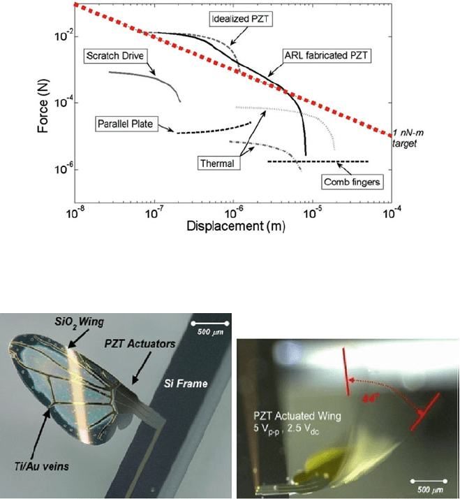
millimeter-scale robotics. The actuation potential of PZT thin-film actuators is best
represented in Fig. 5.63. As illustrated, PZT actuators are capable of achieving
forces and displacement values in excess of other common actuation technolo-
gies for a given footprint. This particular actuator technology is being developed
to enable ground mobile millimeter-scale robotics using a thin-film lateral actua-
tion technology. This lateral actuation technology is created using manipulation of
the PZT thin film relative to the neutral axis position of the beam actuator [16].
Such actuators can achieve mN force levels at micron displacements. Combining
these actuators with single-crystal silicon tethers and end deflectors, it is possible to
achieve in-plane rotations of 3–5
◦
for a single element. Cascading these structures
enables 45
◦
in-plane rotations. Rotations at these levels begin to approach reason-
able levels for the creation of biomimetic insect structures using a hexapod gate.
Another area of interest for piezoelectric MEMS actuators is in microflight at the
millimeter scale. For this application, actuators are being designed to create both
the flapping and angle of attack motions used for flight by insects [84]. As shown
in Fig. 5.64, wing actuators based on PZT thin films have been fabricated using a
combination of surface and bulk micromachining techniques to yield wings capable
of nearly 45
◦
of total angular deflection at 5 V at a resonance frequency of 156 Hz.
These wing actuators are approaching the metrics of many millimeter-scale insects
for flight, including resonance frequencies in the 150–250 Hz range. Total angular
deflection still requires additional research, as values in the range of 80–180
◦
are
desirable to achieve sustainable flight.
One of the key limitations of electrostatically actuated MEMS switches is the
inability to combine a low actuation voltage with excellent DC and RF performance
(i.e., contact force and insertion loss, respectively) and reliability. Attempts to lower
the actuation voltage with electrostatic switches generally rely on reducing either
336 R.G. Polcawich and J.S. Pulskamp
Fig. 5.63 Force-displacement plot of various actuation technologies for actuators confined to a
500 × 500 μm
2
area. The straight line marks the target 1 nN-m minimum performance for mm-
scale robotic applications [16] (Reprinted with permission. Copyright 2008 IEEE)
(a) (b)
Fig. 5.64 Images of a PbZr
1−x
Ti
x
O
3
(PZT) microelectromechanical systems actuated microwing
(2.5 mm length) (a)at0Vand(b) at resonance (156 Hz, 5 Vp-p), showing that resonant behavior
amplifies the stroke. p-p, peak-to-peak [16] (Reprinted with permission. Copyright 2009 IEEE)
the mechanical stiffness of the released structures or the gap between the mechan-
ical bridge/cantilever and the corresponding biasing pad [200]. Reductions in the
stiffness can limit the restoring force of the switch and can lead to stiction failures
[201]. Decreasing the electrode gap limits the high-frequency RF performance (in
particular, the isolation in the open state for series switches) [202].
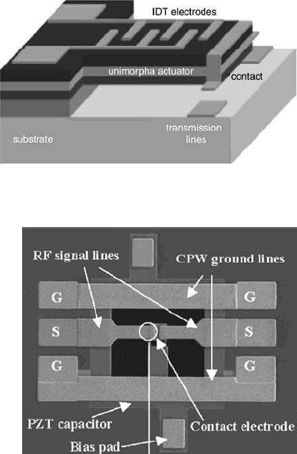
The first functioning piezoelectric MEMS DC relays were demonstrated by
Gross et al. using in-plane poled PZT film actuators [203]. These devices used a
cantilever beam with a supporting elastic layer, a PZT thin film as the actuator, and
patterned gold structures to act as the electrodes (see Fig. 5.65). This device operated
5 Additive Processes for Piezoelectric Materials 337
Fig. 5.65 Illustration of a
thin-film PZT unimorph
switch developed at Penn
State University [203]
(Reprinted with permission.
Copyright 2003 American
Institute of Physics)
Fig. 5.66 SEM image of a
bulk micromachined RF
MEMS series switch using a
thin-film PZT actuator to
complete the signal path
[204] (Reprinted with
permission. Copyright 2005
IEEE)
as low as 20 V with a switching-on time as low as 2 μs. The first reported working
RF MEMS switch using PZT thin films used bulk micromachining to release a uni-
morph actuator and a suspended transmission line [204, 205]. This design utilized
a cantilever perpendicular to the wave propagation direction along the RF conduc-
tor of the coplanar waveguide (CPW). The switch operates as low as 2.5 V with an
insertion loss better than 0.7 dB and isolation better than –21 dB up to 20 GHz (see
Fig. 5.66).
One limitation with the RF switch actuators described above is the require-
ment for bulk micromachining. Surface micromachining is substantially cheaper
and easier to integrate with other fabrication processes than bulk micromachining
techniques [206]. The development of a surface micromachined, piezoelectric RF
MEMS switch is discussed in full detail in the remainder of this section heavily
leveraging the information described in [29, 182].
338 R.G. Polcawich and J.S. Pulskamp
5.3.5 Case Study on the Design and Processing of a RF MEMS
Switch Using PZT Thin-Film Actuators
The first few considerations for the design of a MEMS switch with PZT actuators
are the position of the actuator relative to the microwave transmission line and the
contact configuration. Referencing the description in Section 5.1.3.6, thin-film PZT
generates an in-plane compressive strain at large electric field values when used in
a parallel plate configuration (d
31
mode). The resulting direction of actuation for a
thin-film actuator is dictated by three main parameters, the magnitude and sense of
the transverse piezoelectric stress constant, e
31,f
induced strain (force), and the posi-
tion of the geometric midplane of the piezoelectric thin film relative to the composite
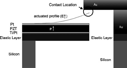
neutral axis (moment arm). If the geometric midplane of the piezoelectric layer lies
above the neutral axis, the induced piezoelectric strain will deflect the actuator up
out of the wafer surface. Using this configuration, a switch can be designed with the
electrical contacts of the switch residing above the actuators (see Fig. 5.67).
Fig. 5.67 Cross-section
schematic of a PZT actuator
and electrical contacts
configured for use as switch
Another important consideration is that the PZT actuator is a multilayer compos-
ite comprised of at least four layers (elastic layer, metal, piezoelectric, metal) with
each layer having significantly different coefficients of thermal expansion (CTE)
and residual stress. The net result of such a structure is the potential for significant
residual-stress-induced deformations in the unbiased actuator state and thermally
induced deformations from the differences in CTE. The reader is directed to Section
5.3.3 for a description of the residual stress gradient and thermally induced stress
deformations. For proper switch operation, a negative static curvature is desired
and can be reproducibly fabricated using an elastic layer comprised of a three-
layer composite of PECVD, SiO
2
, and Si
3
N
4
. The negative curvature using an
oxide/nitride/oxide elastic layer for the actuator not only enables switch opera-
tion with a normally open switch state but also ensures that thermally induced
deformations do not cause the switch to open or close inadvertently.
With the design of the actuator complete, the RF transmission line should be
designed to accommodate the actuator with minimal perturbation to the RF signal.
Based on previous discussions on the piezoelectric strain generation in a parallel
plate capacitor configuration, the switch contacts should be configured above the

5 Additive Processes for Piezoelectric Materials 339
actuators using the vertical motion generated in the actuators. The placement of the
actuators requires a close interaction between the mechanical design and the high-
frequency design aspects of the RF transmission line. By placing the actuators in the
gaps between the RF conductor and ground planes in a coplanar waveguide (CPW)
transmission line, the high dielectric constant PZT combined with the air cavity
beneath the released actuator (created with a XeF
2
etch) can be compensated with
minor changes in the CPW dimensions (i.e., width of the RF transmission line and
RF-GND gap) so as to maintain a 50 impedance in the switch (see Table 5.13 and
Fig. 5.68). The two actuators residing in the RF gaps can be connected mechanically
with a coupling beam containing a short section of conductor used to complete the
RF circuit. Two very short cantilevered structures anchored to each section of RF
conductor overhang the conductor on the mechanical coupling beam and allow the
switch structure to close the series configured gap upon actuation. Another design
feature is air bridges that span the RF conductor to electrically connect each of the
actuators. The actuator bias lines allow the actuation voltage to be applied indepen-
dently of the RF conductor. The bias air bridges spanning the RF conductor require
the width of the conductor to be modified to maintain 50 impedance because of
the capacitive loading on the RF conductor. Thus, the RF conductor is narrowed
underneath the bias air bridges and widened in the regions where the PZT actuators
are located (see Fig. 5.68). It can be compensated with minor changes in the CPW
gaps so as to maintain a 50 impedance.
Table 5.13 Dimensional information for a PZT switch design using a CPW transmission line
Feature Width (μm) Length (μm)
RF conductor (outside of actuators) 75 >150
RF conductor (under air bridges) 50 10
RF gap (between actuators) 40
RF gap (outside of actuator regions) 50
Ground plane 440 660
PZT actuator 40 100, 125, 150
RF cantilever (in) 100 37.5
RF cantilever (out) 75 37.5
RF contact pad (in) 120
RF contact pad (out) 77
Bias air bridges 170 10
Ground straps 18 80
The fabrication of the PZT switch begins with the choice of an appropriate sub-
strate for high-frequency performance and reasonable piezoelectric properties in the
PZT thin film. The preferred substrate is silicon because of the wealth of knowledge
regarding fabrication processes as well as previous history with processing PZT thin
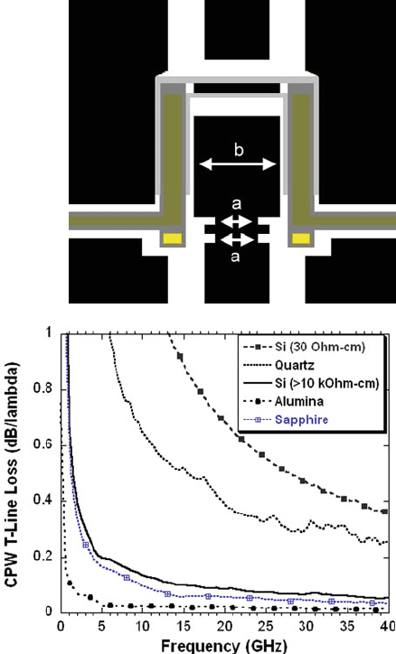
films on platinized silicon substrates. However, as illustrated in Fig. 5.69, a standard
resistivity (1–30 cm) silicon substrate has extremely poor transmission line loss
at microwave frequencies. Traditional microwave substrates, alumina and sapphire
[202], have transmission line losses less than 0.04 dB/wavelength (see Fig. 5.69).
340 R.G. Polcawich and J.S. Pulskamp
Fig. 5.68 Illustration of the
RF conductor width
modifications to account for
(a) capacitive loading from
the DC bias air bridges and
(b) the changes to the
capacitance within the RF
gap from the air cavity
underneath the actuators and
CPW transmission line
Fig. 5.69 Coplanar
waveguide transmission line
(T-line) loss as a function of
frequency for various
substrates. Note: The alumina
is a polycrystalline substrate
Even though high-resistivity silicon is not commonly thought of as a microwave sub-
strate, it performs quite well, with a transmission line loss of ∼0.05 dB/wavelength
at 40 GHz. The transmission line loss is reported as dB/wavelength and not dB/mm
because the primary aim of MEMS switches is in distributed RF circuits. As a con-
sequence, the interest is in designing the smallest low-loss circuits such as phase
shifters and tunable antenna receivers. As the microwave wavelength depends on
the dielectric constant of the substrate, other substrates such as quartz and fused sil-
ica usable for transmitting energy point-to-point, where dB/mm is important, require
much larger circuits to maintain a particular wavelength. The result is that the line
loss per wavelength increases. For the following discussion, high resistivity (>10 k
cm) Czochralski-grown (100) silicon substrates are s elected for fabrication of a PZT
switch.

5 Additive Processes for Piezoelectric Materials 341
Table 5.14 Plasma-enhanced chemical vapor deposition parameters for silicon dioxide and
silicon nitride thin films deposited using a plasma-Therm 790
Material
SiH
4
in
5% He
(sccm) He (sccm)
N
2
0
(sccm) N
2
(sccm)
NH
3
(sccm)
Pressure
(mT) Temp (ºC)
Power
(W)
SiO
2
70 93 390 0 0 900 250 25
Si
3
N
4
90 488 0 160 3.00 900 250 45
The next step in the actuator fabrication is deposition of the stress engineered
elastic layer comprised of SiO
2
/Si
3
N
4
/SiO
2
. The previous discussions regarding this
elastic layer combination are based on PECVD-deposited films deposited at 250
◦
C
using the deposition parameters in Table 5.14. One concern with PECVD films used
in conjunction with higher temperature processing is the release of trapped hydrogen
within the films, especially when using silane (SiH
4
) as a precursor gas. With the
CSD PZT having a thermal budget of 700
◦
C, any trapped hydrogen within the film
must be released prior to deposition of the metal and PZT layers. Following PECVD
deposition, the elastic layer is annealed at 700
◦
CinflowingN
2
(∼5 sccm) for 60 s
to eliminate loosely attached hydrogen ions [207–209]. The hydrogen release also
results in a restructuring of the atomic bonds within the film, altering the residual
stress within the PECVD films leading the values reported in Table 5.12.
Following the elastic layer, the base metal layer of Ti/TiO
x
/Pt is deposited,
preferably using sputter deposition to achieve a high degree of (111) texture in the
Pt. The details of the deposition process for achieving a highly textured Pt layer can
be best described in [158]. The process begins with the deposition of Ti followed
by an oxidation anneal to convert the titanium into titanium dioxide configured in
the rutile crystal structure. The 820 Å Pt layer is then sputter-deposited at 500
◦
C.
With the processing temperature for the PZT being 700
◦
C, the residual stress within
the Pt should be characterized following an anneal at 700
◦
C. The anneal results in
a stress relaxation of the metal thin films, with an increase in the tensile stress of
the metal layer (see Fig. 5.56). However, for device fabrication, the anneal is elim-
inated to ensure optimal growth of the PZT thin film without the introduction of Pt
hillocks.
The planar depositions of the actuator materials are completed with the deposi-
tion of the active piezoelectric layer, PZT (52/48), followed by a sputter deposition
of Pt. For the devices demonstrated in [29], a 0.5 μm thick PZT layer was deposited
via sol-gel using a 2-methoxyethanol solvent-based solution. Sputtered PZT (52/48)
has also successfully been used to create the same switch actuators. After the PZT,
a0.1μm thick Pt layer is sputter-deposited at 300
◦
C.
The next steps in the switch fabrication include actuator patterning, patterning
the RF transmission lines, creation of air bridge structures, and device release and
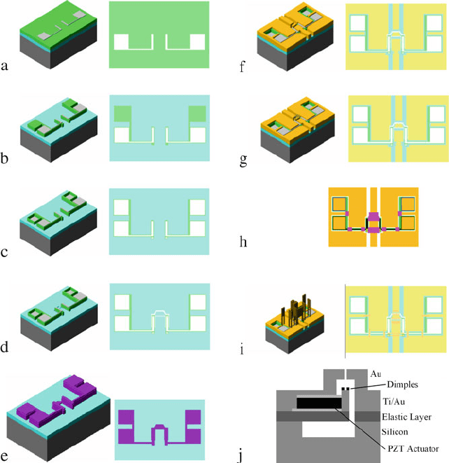
are schematically represented in Fig. 5.70. The actuator patterning begins by defin-
ing the area of the top Pt electrode regions using Ar ion-milling. Next, the PZT and
bottom bilayer of Ti/Pt or TiOx/Pt are patterned with ion-milling stopping on the
342 R.G. Polcawich and J.S. Pulskamp
Fig. 5.70 Fabrication process flow schematic for creating a PZT actuated RF MEMS switch: (a)
pattern top Pt, (b) pattern PZT and bottom Pt, (c) open via to bottom Pt, (d) open etch release
trench, (e) thin elastic layer (pink layer is resist), (f) pattern CPW transmission line, (g) deposit
contact dimple metal, (h) pattern sacrificial resist layer, (i) air bridge deposition, patterning, and
O
2
release of sacrificial resist, (j)XeF
2
etch release of actuator [57] (Reprinted with permission.
Copyright 2007 IEEE)
elastic layer with a small amount of overetch into the top of the elastic layer permit-
ted. The opening via to contact the bottom Pt electrode is completed with either a
combination of ion-milling and wet etching or simply a wet etch using a combina-
tion of H
2
O:HCl:HF (2:1:0.04). The final step required for patterning the actuator
is the opening of the etch trench in the elastic layer surrounding the actuator. This
etch utilizes a combination of CF
4
,CHF
3
, and He to remove the elastic layer and
provide a shallow overetch into the silicon substrate.
Prior to deposition of the RF transmission lines, the remaining elastic layer is
thinned using a combination of CF
4
,CHF
3
, and He to remove the top layer of
5 Additive Processes for Piezoelectric Materials 343
silicon dioxide, silicon nitride, and 50 nm of the bottom silicon dioxide layer. As
described in [29], this etch is crucial for reducing the parasitic and achieving low
loss transmission lines. The transmission lines are patterned using a metal liftoff
technique with evaporated Ti/Au (20/730 nm). In addition, a separate layer of Au/Pt
(400/100 nm) or Au/Ru (400/100 nm) is deposited to serve as contact dimples for
the switch.
The air bridge structures are created using a combination of a sacrificial pho-
toresist layer using a mild high-temperature bake to round the corners of the resist
followed by metal liftoff of an electron-beam-evaporated 2 μm Au layer. The resist
is then removed using an oxygen plasma to then create the free-standing air bridge
structures for the switch. Prior to the final release of the actuators, a short plasma
etch using a combination of CF
4
,CHF
3
, and He is used to remove any oxidation
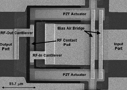
on the exposed silicon surfaces. The final device (see Fig. 5.71) etch is completed
using a timed XeF
2
designed to provide an approximate lateral undercut of 35 μm.
Fig. 5.71 SEM image of a
PZT-actuated RF MEMS
switch [57] (Reprinted with
permission. Copyright 2007
IEEE)
5.4 Summary
This chapter has introduced the fundamentals of piezoelectric and ferroelectric
materials, provided simple models for the response of thin film piezoelectric
devices, and presented an overview of applications for these devices. The mate-
rial deposition and patterning techniques for the polar piezoelectric materials, AlN
and ZnO; and the ferroelectric material PZT have been reviewed. Device design
considerations related to processing have also been addressed for these materials.
Examples and discussions of demonstrated devices and their fabrication processes
have been presented for both polar and ferroelectric materials.
The motivation to overcome the processing challenges with these materials con-
tinues to gain momentum as piezoelectric MEMS devices continue to demonstrate
unique capabilities and in many cases superior device performance. Many of the
