Ghodssi R., Lin P., MEMS Materials and Processes Handbook
Подождите немного. Документ загружается.

314 R.G. Polcawich and J.S. Pulskamp
through the d
31
coefficient in c-axis-oriented AlN films. In a typical two-port config-
uration, an input broadband RF signal is transduced into the mechanical domain via
the converse piezoelectric effect by an input transducer. The signal is then largely
filtered by the mechanical frequency response of the structure and subsequently
transduced back into the electrical domain by means of the output transducer. The
input transducer effectively behaves as an actuator whereas the output transducer
behaves as a sensor. Different resonator geometries are utilized to achieve the best
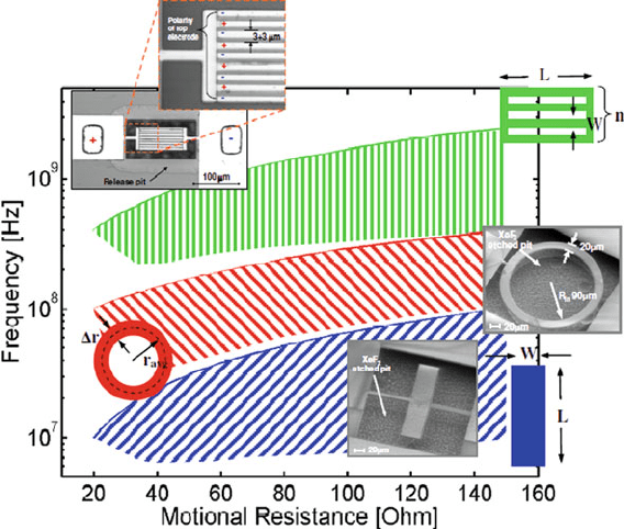
RF performance at various frequencies, including the rectangular plate geometry
(∼10 to ∼100 MHz operation), ring resonators (∼100–400 MHz), and higher-order
contour-mode plate geometries (see Fig. 5.43). These devices have been demon-
strated at frequencies from 20 MHz to about 700 MHz with quality factors as high
as 4300 (230 MHz) and with low motional resistances ranging from 50 to 700 .
Fig. 5.43 Plot illustrating suggested geometries for AlN RF MEMS contour-mode resonators for
various frequency ranges [135] (Reprinted with permission. Copyright 2006 IEEE)
These resonators have also been successfully implemented as bandpass filters
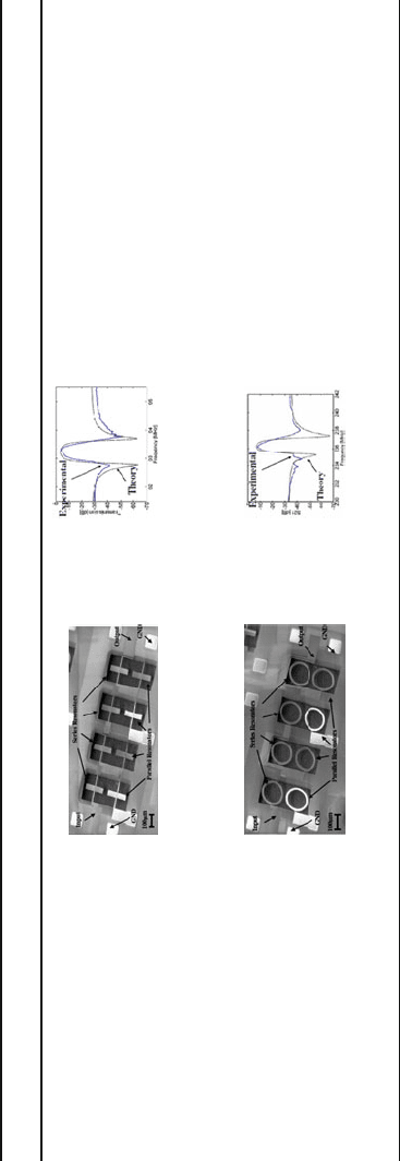
[128]. Electrically coupled resonators, in a ladder configuration, have been demon-
strated with rectangular plate resonators at 93 MHz and with ring resonators at
236 MHz (see Table 5.8). The filters are comprised of individual series and shunt
one-port resonators configured as cascaded L networks. Within each L network,
the series resonance of the series resonator is designed to coincide with the par-
allel resonance of the shunt resonator in order to optimally form the passband of
5 Additive Processes for Piezoelectric Materials 315
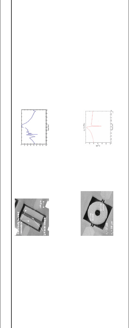
Table 5.8 Summary of performance of AlN contour-mode resonators [1]
Filter Photograph Data Performance
Electrically coupled ladder [9]
f
0
∼ 93.2 MHz
BW
3dB
∼ 305 kHz
%BW
3dB
∼ 0.33%
BW
20dB
∼ 671 kHz
I.L. ∼ –4 dB
Rejection ∼ 27 dB
R
term
∼ 2k
Electrically coupled ladder [9]
f
0
∼ 236.2 MHz
BW
3dB
∼ 605 kHz
%BW
3dB
∼ 0.26%
BW
20dB
∼ 1.8 MHz
I.L. ∼ –7.9 dB
Rejection ∼ 26 dB
R
term
∼ 1k
316 R.G. Polcawich and J.S. Pulskamp
Table 5.8 (continued)
Filter photograph Data Performance
Mechanically coupled array [10]
f
0
∼ 40 MHz
BW
3dB
∼ 392 kHz
%BW
3dB
∼ 0.98%
BW
20dB
∼ 1.1 MHz
I.L. ∼ –1.5 dB
Rejection ∼ 20 dB
R
term
∼ 1.5 k
Dual mode resonator [1]
f
0
∼ 22.4 MHz
BW
3dB
∼ 112 kHz
%BW
3dB
∼ 0.5%
BW
20dB
∼ 358 MHz
I.L. ∼ –4.8 dB
Rejection ∼ 30 dB
R
term
∼ 2.5 k
Reprinted with permission. Copyright 2006 IEEE
5 Additive Processes for Piezoelectric Materials 317
the filter. The bandwidth of the filter is related to the difference between the series
resonance of the shunt resonator and the parallel resonance of the series resonator.
This requires a frequency shift between the two resonators, within each L network,
by as much as a few percent and as little as a few tenths of a percent. Piazza, et al.
[128] accomplished this by modifying the geometry of the bottom Pt electrode to
affect mass loading of the composite resonators between the series and shunt devices
within the filter. These devices show very good RF performance with further gains
expected with optimization. The rectangular plate-based filters, featuring eight res-
onators, display 4 dB of insertion loss and 27 dB of out-of-band rejection at 93 MHz
with 2 k termination resistances. The filters based on eight ring resonators display
8 dB of insertion loss and 26 dB of out-of-band rejection at 236 MHz with 1 k
termination resistances.
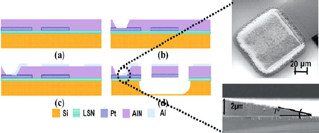
The fabrication of these AlN contour-mode filters utilizes a four-mask CMOS
compatible process (see Fig. 5.44). The process begins with the deposition of a
LPCVD l ow-stress nitride buffer layer onto a silicon substrate. A 100 nm RF sput-
tered Pt bottom electrode layer is patterned by liftoff. The AlN films are deposited
with a single-module Advanced Modular Sputtering (AMS, Goleta, CA) PVD sput-
ter tool. Bottom electrode vias through the AlN film are defined with a wet etch
of heated phosphoric acid. The wet etch provides a modest slope etch profile,
facilitating the ensuing top electrode contact required for properly configuring the
series and shunt resonators of the filter. A dry etch is used to define the top Al
electrode. The AlN layer is patterned with a hard mask of low-temperature oxide
and a chlorine-based dry etch. In addition, the top electrode is passivated by a
∼30 nm layer of Nb during the AlN etch step. The Nb l ayer, remaining LTO
hard mask, and the low-stress nitride layer beneath the resonators are removed
during the subsequent CF
4
-based dry etch. Finally, xenon difluoride is used to
release the devices and to remove any remaining low-stress nitride from beneath the
resonators.
Fig. 5.44 Illustration of the fabrication process used to demonstrate AlN electrically coupled fil-
ters and images of the wet etch bottom electrode via [128] (Reprinted with permission. Copyright
2007 IEEE)
318 R.G. Polcawich and J.S. Pulskamp
5.3 Ferroelectrics: PZT
This section concentrates on the leading ferroelectric material used in thin-film
piezoelectric MEMS: lead zirconate titanate (PbZr
x
Ti
1−x
O
3
) or PZT. Possessing a
piezoelectric coefficient nearly an order of magnitude larger than its nonferroelectric
counterparts, PZT is the ideal candidate for devices requiring large displacements
or forces. The goals of this section include an analysis of the deposition of these
materials, patterning techniques, identification of device design and processing con-
cerns, and finally a detailed subsection covering examples of PZT devices including
a case study on PZT actuators for RF switching applications.
5.3.1 Material Deposition
PZT thin films have been successfully deposited by a wide variety of processes
with a majority of the early development done through various sputtering techniques
with a strong focus on RF or ion-beam deposition using bulk ceramic targets [136–
139]. Current research efforts primarily utilize sputtering [140, 141], metal-organic-
chemical vapor deposition (MOCVD) [142–144], and chemical solution deposition
techniques [145–151] with many of the techniques summarized in Table 5.9.PZT
deposition methods require strict control of the stoichiometry to prevent nucleation
of nonferroelectric fluorite and pyrochlore structures [ 152, 153]. Furthermore, lead
oxide (PbO) becomes highly volatile above 500
◦
C so one must take care to provide
enough excess lead to compensate f or lead loss through the release of PbO during
any high-temperature processing and annealing [154].
A variety of substrates can be used for PZT deposition. However, there are
requirements for both the substrate and/or metallization layers. Growth of PZT is
strongly nucleation controlled and with proper control of the nucleation, crystal
orientation of the film can be manipulated [155, 156]. Single crystal substrates (i.e.,
MgO, SrTiO
3
) can be used to nucleate epitaxial, single-crystal PZT thin films [157].
For most MEMS applications, silicon is the substrate of choice. When using Si
it is important to prevent the formation of lead silicide at t he substrate interface by
using buffer layers and/or metal layers. In most instances, a layer of silicon diox-
ide is used as a buffer layer in combination with a bilayer of Ti/Pt to serve as the
base electrode for the PZT deposition. With the lattice constant of platinum being
close to that of PZT (2–3% mismatch for c-axis-oriented PZT), Pt can be an excel-
lent template for (111) oriented PZT films as Pt tends to grow with a strong (111)
texture. In order to maximize the texture within the Pt, the preferred material stack
is SiO
2
/TiO
x
/Pt [158]. The layer of TiO
x
serves as a buffer layer and template that
allows a higher degree of texture within the Pt. For detailed information on the
method required for achieving highly textured (111) Pt, the readers are directed to
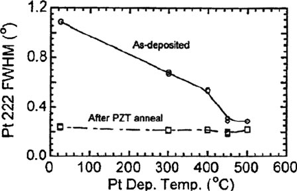
[158] with one of the key figures reproduced in Fig. 5.45. Methods of manipulat-
ing the texture of the PZT away from (111) orientation when using Pt layers are
discussed later within this section.

5 Additive Processes for Piezoelectric Materials 319
Table 5.9 Deposition methods and parameters for PZT thin films
Deposition parameter DC sputter (reactive) RF sputter MOCVD MOCVD CSD
Target stoichiometry Pb, Zr, Ti (3 metal targets) Pb
1.20
(Zr
0.53
Ti
0.47
)O
3
Excess Pb % 20 10 and 30
RF power (W) 100
Bias (V or W)
Pressure (Pa or T) 1–2 5 T
Gas O
2
(1–3 sccm) O
2
(1 L/min) O
2
Deposition rate (nm/min) 10–20 12
Temperature (
◦
C) 570 followed by post-dep RTA 550–700 550 540 RT→350
→650
References [140][140, 160][144][143][149]
320 R.G. Polcawich and J.S. Pulskamp
Fig. 5.45 Texture, FWHM of
the sputtered Pt (222) peak,
as a function deposition
temperature and after thermal
processing of a PZT film
deposited atop the Pt film
[158]
There are several metal and/or conducting oxides (i.e., Ru and RuO
2
and Ir and
IrO
2
) that can be used in place of Pt. These alternative electrodes can exhibit a higher
resistance to Pb interdiffusion and thus provide a better barrier. Oxide electrodes are
commonly used for the top electrode to reduce ferroelectric fatigue (reduction of
switchable polarization with bipolar cycling). Note, ferroelectric fatigue has very
little dependence on the bottom electrode material. In a vast majority of MEMS
applications, bipolar switching will be avoided with typical operation relying on
unipolar drive (see Section 5.1.3.10).
Sputter deposition of PZT thin films has been completed through either reactive
deposition using three metal targets (Pb, Zr, and Ti) or RF sputtering using ceramic
targets. In either case, PZT thin films with excellent ferroelectric and piezoelectric
properties can be obtained. One challenge with sputter deposition is accurate con-
trol of the Pb and O content within the films. Lead has a higher sputter yield and
higher volatility (i.e., PbO) compared to Zr and Ti. As a result, the lead loss must
be compensated with either higher fluxes sputtered from pure Pb targets or excess
Pb incorporated in ceramic targets. An additional item of note is the substrate tem-
perature during deposition. The use of high temperatures during deposition results
in higher Pb loss and typically requires higher excess lead content targets. If the
substrate temperature can be maintained greater than 600
◦
C, pure perovskite-phase
PZT thin films can be achieved. Otherwise, a crystallization anneal is required
on the sputtered film to convert the deposited layer into the desired perovskite
phase.
MOCVD processes for PZT thin films have been researched as a key technology
for mass production of ferroelectric random access memory (FeRAM) especially for
device architectures requiring exceptional step coverage. For PiezoMEMS applica-
tions, there has been limited information reported on the piezoelectric properties
MOCVD-deposited thin films. For a summary of the MOCVD deposition process
readers are directed to [142, 144] for more detail.
Chemical solution deposition (CSD) methods for ferroelectric thin films have
been developed based on a variety of methods (i.e., sol-gel and metallorganic
decomposition) and precursors [159]. The CSD techniques can be categorized into
5 Additive Processes for Piezoelectric Materials 321
three main groups: sol-gel, chelating process, and metallorganic decomposition
[149, 150]. The two most widely used approaches are based on a sol-gel approach
using 2-methoxyethanol as a solvent and the inverted mixing order process using
methanol as a solvent. Sol-gel methods have been primarily based on the research
of Budd et al. in 1985 [145].
With the inverted mixing order (IMO) process, the lead, titanium, and zirconium
precursors are combined in the opposite order from those developed in the original
sequential addition process by Budd et al. [145, 160, 161]. In addition, the solvent
used for the IMO process is methanol with slight additions of acetic acid and deion-
ized water for additional solution stability. The use of methanol instead of 2-MOE
enables a less toxic solution preparation and deposition process for the user [159].
The most heavily researched processes for the deposition of PZT films uses 2-
MOE as a solvent and lead acetate trihydrate, titanium iso-propoxide, and zirconium
n-propoxide as the precursors [145, 162, 163]. This process has been used to pro-
duce PZT films with the highest piezoelectric coefficients to date. A general version
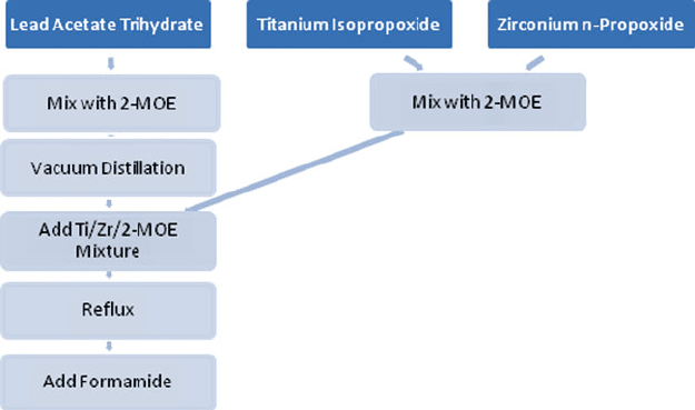
of the 2-MOE-based solution process flow is highlighted in Fig. 5.46.Tobegin,the
lead precursor (lead acetate trihydrate) is dissolved in 2-MOE followed by vacuum
distillation to remove the water. The dehydrated lead acetate is allowed to redissolve
in a portion of the 2-MOE solvent before being mixed with the Zr and Ti precur-
sors. Prior to being added to the lead precursor, the Zr and Ti precursors are mixed
in the desired stoichiometric ratio at room temperature with 2-MOE. The combined
solution is refluxed for 2–3 h at 120
◦
C using a rotary evaporator or comparable
setup. Next, the solution undergoes a short vacuum distillation to remove a small
amount of reaction by-products and adjust the concentration, typically 0.4 M. The
final step is to add 4 volume percent of formamide, which serves as a drying control
Fig. 5.46 Schematic process flow for creating a 2-MOE-based solution for PZT thin films
322 R.G. Polcawich and J.S. Pulskamp
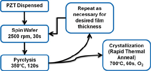
Fig. 5.47 Deposition and thermal treatment process flow for chemical solution deposition of PZT
thin films based on a 2-Methoxyethanol solvent system
agent [164]. Additionally, a small percentage of acetylacetate may be added to the
solution to assist in the long-term stability of the solution [165].
Regardless of the solution chemistry, the deposition processes are quite sim-
ilar and graphically represented in Fig. 5.47. The only discrepancies are minor
changes to the pyrolysis temperature or the crystallization temperature. The depo-
sition begins by placing the solution into a syringe configured with a 0.1–0.2 μm
PTFE (polytetrafluoroethylene) filter. The solution is statically dispensed onto t he
substrate and then spun to achieve a uniform film thickness across the substrate.
Following the spin, the film is pyrolyzed on a hot plate to remove the volatile organ-
ics. The spin and pyrolysis steps are repeated as required (i.e., one to four layers)
prior to the crystallization anneal in flowing oxygen. Using a 0.4 Molar solution, a
four-layer spin process typically yields a final film thickness close to 0.25 μm. The
process is continuously repeated until the desired film thickness is achieved.
Regardless of deposition method, there are several key material parameters with
which to judge the quality of the PZT thin film. The first is the crystalline quality
of the film via X-ray diffraction (XRD). The best quality piezoelectric films will
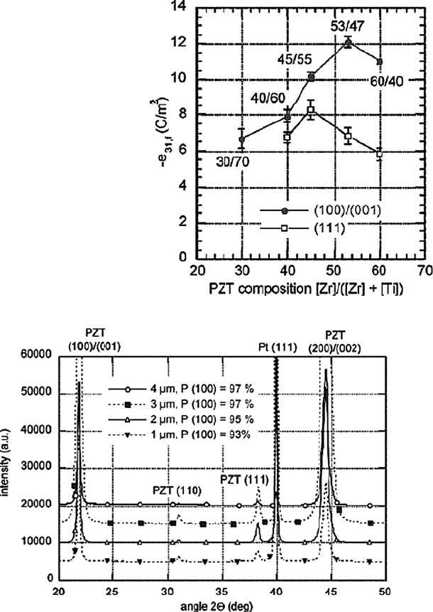
possess a high degree of texture in the (100)/(001) orientation (see Fig. 5.48). The
easiest method of assuring a high degree of (100) texture is through templating the
nucleation and growth with a PbTiO
3
seed layer and proper attention to the amount
of excess lead present during any high-temperature annealing or crystallization pro-
cesses [155, 163]. An example XRD pattern of a highly textured CSD PZT thin film
is shown in Fig. 5.49.
Optimizing material quality and properties requires controlling the stoichiomet-
ric gradients through the thickness of the PZT film. Figure 5.50 illustrates the
importance of controlling these gradients, as these gradients represent deviations
of the average properties of the film from the intended composition. As stated ear-
lier, PZT films are strongly nucleation controlled. With heterogeneous nucleation
occurring at the electrode interface, Ti rich compositions nucleate first [155]. The
end result is a sawtooth Zr/Ti gradient through the PZT thickness with a Ti rich
layer at the electrode interface and a Zr-rich layer at the film surface (see Fig. 5.50)
[149]. To compensate for the gradient, Calame and Muralt developed a process to
5 Additive Processes for Piezoelectric Materials 323
Fig. 5.48 Transverse
piezoelectric stress constant,
e
31, f
,ofa1μm PZT thin film
as a function of Zr/Ti ratio for
both (100)/(001) and (111)
oriented thin films [163]
(Reprinted with permission.
Copyright 2003, Elsevier)
Fig. 5.49 –2 X-ray diffraction pattern for PZT (53/47) thin films (1–4 μm) using a PbTiO
3
seed layer to promote a highly textured (100) orientation [163] (Reprinted with permission.
Copyright 2003 Elsevier)
reduce the gradient by manipulating the stoichiometry of each of the four CSD lay-
ers (63, 58, 48, and 43% Zr content) deposited prior to the crystallization step [149].
As shown in Fig. 5.50, the average composition through the entire 2 μm thickness
closely resembles the MPB desired composition of 53/47.
