Ghodssi R., Lin P., MEMS Materials and Processes Handbook
Подождите немного. Документ загружается.

1134 M.A. Huff et al.
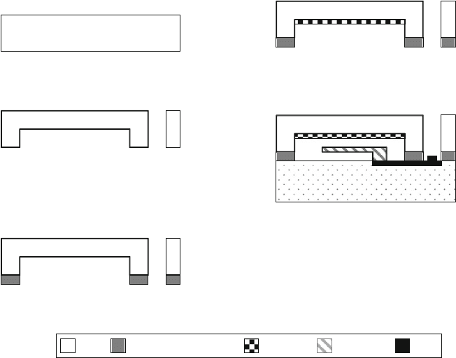
MEMS Device Wafer
(a). Starting silicon or Pyrex capping wafer (we show a
silicon capping wafer through rest of process flow).
Silicon Wafer
(b). Silicon capping wafer is patterned and etched to
form a recess where the MEMS device will be located
and patterned and etched to form a through-via to where
the electrical bond pads on the MEMS device will be located.
We show the use of DRIE to perform these etches, but they
could be performed using any appropriate etching technology.
Silicon Wafer
(c). An sealing material that is appropriate for bonding
the two wafers together is deposited and patterned on the
capping wafer in the area to be sealed around the MEMS device.
Silicon Wafer
(d). The NanoGetter
TM
material is sputter deposited
and patterned in the recess area of the capping wafer.
Silicon Wafer
(e). The capping wafer is bonded to the MEMS
device wafer and the NanoGetter
TM
material is
activated. The wafer is then diced into individual
microchips.
Silicon Wafer
Silicon MetalWafer bonding/Sealing Layer Nanogetter
TM
MEMS Device
Fig. 14.67 Process flow for ISSYS wafer-level packaging process sequence
(Fig. 14.67e). The optimum bonding temperature varies depending on the sealing
materials used, with higher temperatures (up to 425
◦
C) usually necessary for glass
frit bonding processes and lower temperatures for solder bonding processes. After
the MEMS device wafer is bonded to the capping wafer and the gettering material
has been activated, the composite bonded wafer pair is diced into individual die,
which can then be attached and wirebonded or flip-chip bonded to connect to the
intended system.
The material used for bonding the substrate together will play a large part in
determining what kinds of devices can be packaged using this approach. Obviously,
a solder material would be more suitable for the packaging of integrated MEMS
devices because they are more susceptible to degradation upon exposure to higher
temperatures.
14.8.3 Review of Integrated CMOS MEMS Process Technologies
14.8.3.1 iMEMS – Analog Devices
The Analog Devices, Inc. iMEMS process is the evolution of an integrated
MEMS/circuit process that began its development in the late 1980s as a skunk-works
project at Analog Devices, Inc (ADI) [66, 67]. The process was developed to
14 MEMS Process Integration 1135
implement an interdigitated finger-based, variable capacitance accelerometer. The
MEMS unit process steps were developed within a s tandard single-metal 3 µm
BiCMOS process that had been running at ADI for many years. The MEMS struc-
ture portion of the process was a relatively straightforward 2 µm thick polysilicon,
surface-micromachining process. The accelerometer application called for both
thick polysilicon and narrow finger-to-finger gaps, in other words, a large aspect
ratio for the main structural polysilicon etch. In the technology of the time, an aspect
ratio of 1–2 was considered state of the art. The sensor design, with its large num-
ber of positive and negative polarity fixed fingers also required careful design of
vias and electrical interconnect. Because the single metal could only be deposited
at the end of the process for thermal reasons, the sensor interconnect was done with
polysilicon layers and substrate diffusions.
Much of the complexity of the process was driven by the requirements for spa-
tial segregation between the MEMS sensor and the circuitry and by the mechanism
used to support the MEMS structure during release and subsequent process s teps.
The BiCMOS circuit process was fundamentally an analog process, and the bipolar
transistors were the workhorses of the circuit designs. In recent years, the pro-
cess has undergone two major revisions to increase the thickness of the structural
poly-silicon to 4 µm and to include a self-assembled monolayer (SAM) coating for
stiction reduction.
Process Flow Overview
The basic construction of the ADI iMEMS process is:
1. Build the circuit devices.
2. Build the MEMS sensor.
3. Wire the sensor and the circuit.
4. Release the sensor.
Build the Circuits
The BiCMOS process supports NPN and PNP bipolar transistors and PMOS and
NMOS FETs. The process starts with a P+ substrate with a P epitaxial layer. N wells
are defined and implanted to construct PMOS and NPN bipolar transistors. The tran-
sistor process is typical, including a thick oxide growth to separate the transistors.
This thick oxide is also used to define the boundary between the MEMS sensor area
and the circuit area. The first joint process step is an N+ diffusion that forms the
N+ emitter of the NPN transistors and also a conductive interconnect between the
sensor and the circuit areas. The transistor gate oxide is also used in the sensor area
to isolate the N+ diffusion.
Build the Sensor
The sensor construction begins by stripping off the circuit passivation from the
sensor area. A polysilicon ground-plane layer is deposited followed by a 2 µm
1136 M.A. Huff et al.
sacrificial oxide. The thickness of this sacrificial oxide is a critical design parameter,
so considerable care must be taken to understand its deposition, densification, and
etch characteristics. As with other polysilicon surface micromachining processes, a
bump etch is employed to reduce the contact area between the released structure and
the ground plane. Etches must also be made through the sacrificial oxide to allow
contact to the ground plane and the N+ interconnect. Four microns of polysilicon
are deposited to form the released structure (including its anchors). This material is
heavily doped to produce a material that is a good conductor. Deposition and anneal
conditions must be carefully designed to control stress and curvature in the released
film. A dry RIE etch is used to pattern this film.
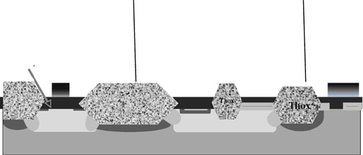
Nwell
Nwell
PMOS
Transistor
NPN Bipolar
Transistor
Sensor
Boundary
Gate Oxide
N+
P+
N+
N+
P+
N+
Thox
Thox
Substrate
Fig. 14.68 The BiCMOS circuit area (Reprinted with permission, copyright Analog Devices Inc.)
Connect the Sensor and the Circuit
This part of the process starts by stripping the sensor sacrificial oxide from the cir-
cuit area. An etch is performed to open N+ diffusion contact areas at the periphery of
the sensor area. Platinum is deposited and sintered to form platinum silicide in t hese
contact areas. TiW is deposited as a barrier metal and then aluminum is deposited
and patterned as in a typical circuit interconnect process.
Release the Sensor
The ADI iMEMS process uses a unique method of depositing and patterning pho-
toresist, which will remain during the sacrificial oxide release etch. The key is that
small, strategically placed areas of the sacrificial oxide are initially etched. These
“holes” are then filled with photoresist, making a solid material between the sensor
polysilicon and the ground plane. These photoresist supports remain in place and
the sacrificial oxide is removed by a wet HF etch and subsequent drying to keep the
sensor polysilicon layer from collapsing due to the very large surface tension forces
associated with the drying process. After the release etch, the process is completed
by depositing a self-assembled monolayer (SAM) coating to reduce stiction forces.
14 MEMS Process Integration 1137
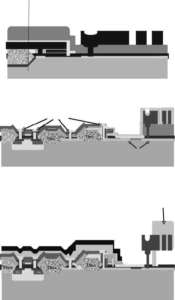
Circuit
Sensor
Thox
Oxide
Polysilicon
Fig. 14.69 Cross-section showing the patterned sensor. Note the via on the sensor that connects it
to the interconnect layer below (Reprinted with permission, copyright Analog Devices Inc.)
P+ P+
TiW/AlCu
Thox
N+ interconnect
Fig. 14.70 Cross-section showing the circuit interconnect. Note that the N+ diffusion forms an
interconnect layer between the circuit and the sensor (Reprinted with permission, copyright Analog
Devices Inc.)
Photoresist
Fig. 14.71 Cross-section showing the final structure. The photoresist shown is removed to com-
pletely release the actuator structure (Reprinted with permission, copyright Analog Devices Inc.)
1138 M.A. Huff et al.
14.8.3.2 DLP (Texas Instruments)
Digital Light Processing technology developed by Texas Instruments Corporation is
one of the most successful MEMS development endeavors to date with market sales
of chip sets of nearly $1 B annually and is used in various large volume commercial
markets such as projection televisions and projection display systems [68, 69]. DLP
technology is a disruptive technology for movie theaters because it replaces the 100-
year old celluloid film with a completely digital format. Already, DLP is currently
used in more than 14,000 theaters, with over 7000 more advanced 3-D systems
deployed in theaters. The key component of DLP
R
technology is the micromir-
ror array chip (called the Digital Micromirror Device, or DMD for short [70]).
Essentially the DMD chip is a large array of individually and digitally controlled
MEMS micromirrors; there are up to 2 M mirrors in each chip array! Each mirror
in the array measures just over 10 µmby10µm and is electrostatically actuated
by the microelectronics physically located underneath the mirror array [71]. This
enables the fill factor of the DMD to reach levels of over 90%, thereby allowing
very high optical efficiency and contrast. Integrated microelectronics is a neces-
sity in DLP technology inasmuch as the number, density, and size of the mirrors
combined with individual addressability would preclude having all the electronics
off-chip. The DMD fabrication is made using a “MEMS last” integrated process
technology wherein the microelectronics are fabricated in the base substrate first
and then the MEMS mirrors are fabricated on the surface of the microelectronics
substrate [72].
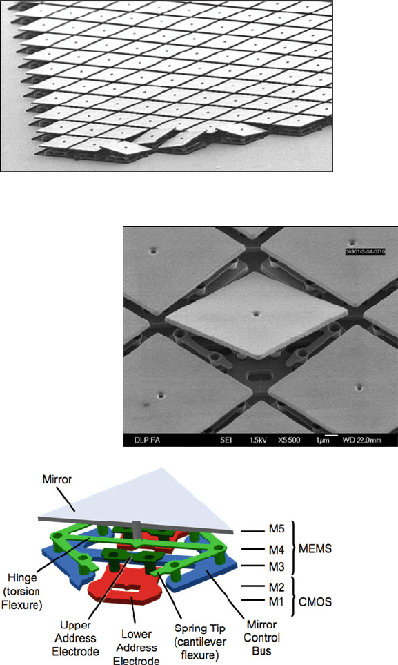
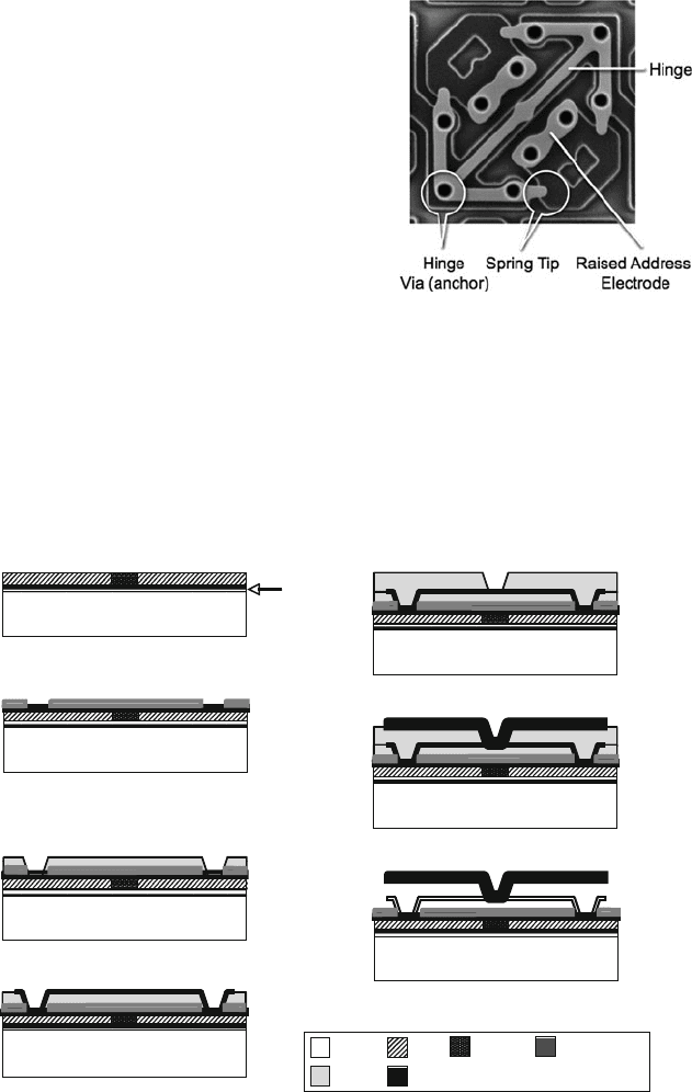
Figure 14.72 is a SEM of a portion of the DMD device and Fig. 14.73 is a closer-
view SEM of the DMD micromirror array showing the center pixel in the actuated
state and the surrounding pixels in the unactuated state. As can be seen, the mirror
rotates by approximately 12
◦
in the actuated state and without actuation the mirrors
(shown around the center pixel) are nominally flat. For a description of how DMDs
are used in projection optical systems, see [70, 72]. The mirrors have a complex
hinge mechanism to allow t hem to rotate by a sufficient angular displacement while
keeping the strain in the hinges to an acceptable level. High levels of reliability
are required for consumer electronics applications, which have been achieved by
having exceptional control to reduce the hinge memory and stiction effects in the
DMD. Remarkably, individual mirrors have been operated over 10
12
full mechanical
movements without failure and thereby have demonstrated an extremely high level
of reliability [68]. Figure 14.74 is a cross-section illustration of the DMD showing
the electromechanical elements underlying a DMD mirror which enable it to actuate
and Fig. 14.75 is a SEM of a pixel with the mirror removed to exhibit the underlying
structure.
The DMD pixel consists of a SRAM cell fabricated in the silicon sub-
strate with a MEMS superstructure implemented on top. The MEMS-last process
sequence requires that all post-CMOS processing steps used to fabricate the MEMS
superstructure be compatible, both thermally and chemically, with the CMOS.
Consequently, the thermal budget for these processing steps is quite restricted
and no processing temperatures can exceed 400
◦
C. This is achieved in the DMD
14 MEMS Process Integration 1139
Fig. 14.72 SEM image of DMD chip shown with the pixels near the leading edge of the array in
the actuated (i.e., nonflat) state (Reprinted with permission, copyright Texas Instruments, Inc.)
Fig. 14.73 Magnified SEM
image of Texas Instrument’s
DMD device with center
pixel in actuated (i.e., rotated)
state (Reprinted with
permission, copyright Texas
Instruments, Inc.)
Fig. 14.74 DMD pixel showing the electromechanical components under the mirror that enables
the device to actuate (Reprinted with permission, copyright Texas Instruments, Inc.)
1140 M.A. Huff et al.
Fig. 14.75 SEM image of a
DMD pixel with the top
aluminum mirror l ayer
removed to expose the
underlying aluminum layers
forming the hinge and
electrode elements (Reprinted
with permission, copyright
Texas Instruments, Inc.)
process sequence by fabricating the MEMS superstructure utilizing a series of rel-
atively low temperature deposition and etch processes. Consequently, the DMD is
made using a low-temperature, surface micromachining, MEMS-last, monolithic,
integrated MEMS process technology.
The DMD process sequence begins (see Fig. 14.76) with a relatively conven-
tional 0.8 µm linewidth CMOS process technology having a two-layer metallization
(M1 and M2) [72]. After the CMOS is completed, a relatively thick oxide layer is
(a). A CMOS wafer having a two-layer metallization (M1 and M2) has a thick
oxide deposited on the surface, followed by CMP to planarize the surface. A
metal plugged via is fabricated through the oxide layer so as to make electrical
connection to the mirror electrodes.
CMOS Silicon Wafer
(b). A so-called “dark” metal layer (M3) is sputter deposited, patterned and
etched to form the lower address electrodes. M3 is composed of a base
aluminum layer, a second high-resistivity layer (shown as part of aluminum
layer), and a thin capping layer of oxide. M3 forms an antireflective coating on
the substrate surface. Contact openings are made in the topmost thin oxide layer
to serve as contacts between the hinge layer (M4) and electrode layer (M3).
CMOS Silicon Wafer
(c). A sacrificial polymer layer is deposited over layer M3 and patterned on
the substrate surface to make a spacer layer and anchors for the MEMS
superstructure.
CMOS Silicon Wafer
(d). Another aluminum layer (M4) is sputter deposited, patterned and etched
to to form the hinge (flexure) for the mirror, the upper address electrodes,
and the anchors that support the hin
g
e at the contact openin
g
to M3.
CMOS Silicon Wafer
(e). Another polymer layer is deposited and patterned on the substrate surface to make
a second spacer layer and via for the mirror center post.
CMOS Silicon Wafer
(f). An aluminum layer (M5) is sputter deposited, patterned and etched to form the
mirror component.
CMOS Silicon Wafer
(g). After dicing, the polymer sacrificial layers are removed using an oxygen plasma
exposure thereby releasing the mirrors.
CMOS Silicon Wafer
Silicon
Oxide
Polymer
Metal Plug
Aluminum
Electrode Oxide
M1 & M2
Fig. 14.76 Texas Instruments’ DMD process technology
14 MEMS Process Integration 1141
deposited on the wafers and subsequently planarized using chemical-mechanical
polishing. The planarization of the surface of the CMOS wafer is very important
to ensure that the wafer surface is completely flat prior to beginning the MEMS
fabrication in order not to degrade the brightness uniformity or contrast ratio of the
DMDs. The CMP oxide layer is patterned, etched, and filled with metal to form
plugged vias to electrically connect the CMOS electronics to the actual mirror bus
lines (Fig. 14.76a).
Next, a so-called “dark” metal layer (M3) is deposited, patterned, and etched to
form the lower address electrodes (Fig. 14.76b). M3 is actually a stack composed
of a base aluminum layer, a second high-resistivity film, and a capping layer of thin
oxide. Together these three layers form an antireflective coating to reduce stray light
reflections from the substrate. Contact openings are then patterned and etched in the
thin cap oxide layer to serve as electrical contacts between the hinge layer (M4) and
electrode layer M3. Next, a planarizing, sacrificial polymer layer is deposited over
the M3 and subsequently patterned (Fig. 14.76c).
Another aluminum metal layer (M4) is then sputter deposited, patterned, and
RIE etched to form the hinge (flexure) for the mirror, the upper address electrodes,
and the anchors that support the hinge at the contact openings to M3 (Fig. 14.76d).
After the hinge metal layer (M4) has been defined, another thick, planarizing sacrifi-
cial layer of polymer is deposited on the wafer surface (Fig. 14.76e). Subsequently,
another aluminum metal layer (M5) is sputter deposited onto the patterned poly-
mer sacrificial layer, followed by the patterning and etching of the aluminum layer
to define the DMD mirrors. After the top metal aluminum layer has been etched
using RIE (Fig. 14.76f), a layer of photoresist is deposited to protect the mirror sur-
faces during dicing (not shown). Lastly, the DMD mirrors are released by placing
the substrates in an oxygen plasma etcher, which removes the sacrificial polymer
layers, as well as the protective photoresist top coat, thereby leaving the functional
MEMS mirrors (Fig. 14.76g) and completing the DMD fabrication.
14.8.3.3 Integrated MEMS Pressure Sensor (Freescale)
The Integrated Pressure Sensor (IPS) process technology was originally devel-
oped and put into production by Motorola (now Freescale Semiconductor) in 1991
and represents one of the most successful and long-standing high-volume MEMS
products in the commercial market. The device is mostly used in automotive appli-
cations, but is also employed in medical devices and industrial control applications.
This sensor employs the piezoresistive effect to measure the deflection of a thin
silicon membrane and combines bipolar microelectronics for signal conditioning
and calibration on the same silicon substrate as the sensor device, thereby making
it a fully integrated MEMS product (actually the first fully integrated high-volume
MEMS product since it went into production in 1991). The transduction approach
taken to measure membrane deflection under pressure loading is somewhat unusual
inasmuch as it uses a single piezoresistor element to measure strain as opposed
to the conventional approach of using multiple, distributed piezoresistors (e.g.,
Wheatstone bridge). Freescale has used two types of piezoresistive transducers, the
1142 M.A. Huff et al.
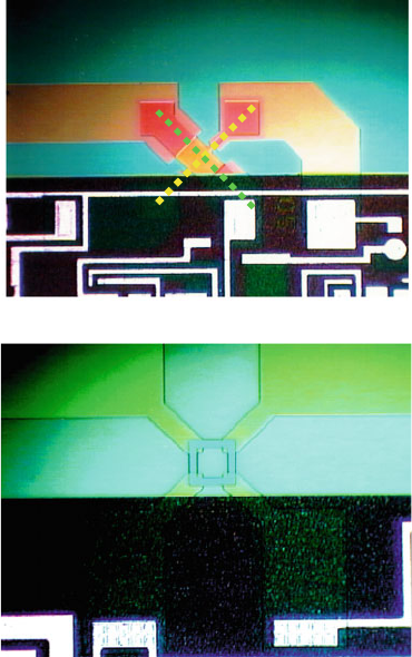
(a)
(b)
Fig. 14.77 (a) Optical
photograph of top surface of
Freescale pressure sensor that
employs the original X-ducer.
An “X” has been added to
show the transducer layout.
(b) The newer “picture
frame” piezoresistor
configuration (Reprinted with
permission, copyright
Freescale Semiconductor
Inc.)
X-ducer
TM
and the Picture Frame. The original “X-ducer” design resembles an “X”
located at the edge of the pressure deflecting membrane (Fig. 14.77a). The X-ducer
design had the benefit of reducing the offset distribution that is an undesirable
attribute of some Wheatstone bridges.
The process technology has been improved over the years, tracking recent devel-
opments in micromachining and design, and Freescale now uses what is called a
“picture frame” piezoresistor configuration that allows approximately 40% greater
output signal than the X-ducer design (Fig. 14.77b). Other process improvements
include using an electrochemical etch stop to precisely control the pressure-sensing
membrane thickness and reduction of the area consumed by the sensor [73]. We
review the most recent process flow for this device.
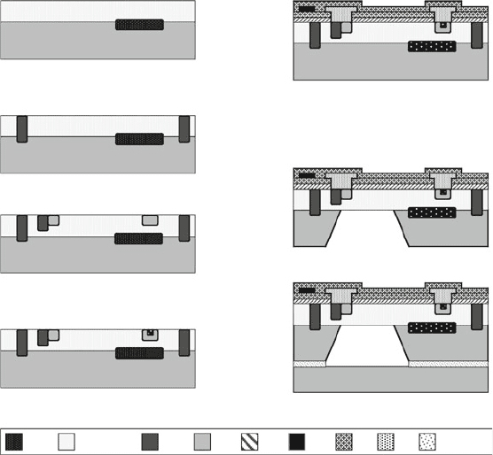
The process begins with a single crystal p-type silicon substrate (Fig. 14.78)
[74]. A diffusion to create an n+ region is performed and this will be used to form
the buried layer for the bipolar transistor devices. A 15 µm thick layer of n-type
silicon is epitaxially grown on the surface of the wafer and this is followed by
a deep diffusion to create p+ regions to electrically isolate the bipolar transistors
(Fig. 14.78a, b). Subsequently, a diffusion is performed to create a p+ region that
14 MEMS Process Integration 1143
Silicon Wafer
Starting wafer p-type silicon substrate, followed by n+
diffusion to create bipolar buried layer. Then a 15 micron
thick layer of n-type silicon is deposited using epitaxy.
Silicon Wafer
Deep p+ diffusions are performed to form isolation
for the bipolar transistors.
Silicon Wafer
A p+ diffusion is performed to form low-resistance
connections and a p- diffusion is performed to make the
piezoresistor element.
Silicon Wafer
A n+ diffusion is performed to form emitter for
bipolar transistor formation.
Silicon Wafer
Chrome silicide resistors are formed that will be laser-trimmed
to calibrate the pressure sensor after packaging. Then a 1.5
micron thick aluminum layer is deposited and patterned to
electrically contact and connect the devices. A passivation
layer of silicon nitride is then deposited using PECVD. The
SiN is removed from the bond pads.
Silicon Wafer
A backside wet anisotropic etch is performed using an
electrochemical etch stop created by biasing the epi layer.
Silicon Wafer
Optional: a wafer is bonded to the backside using glass frit to
create a sealed reference cavity for absolute pressure sensor.
Reference
Cavity
CrSip+ Si Al Glass Fritp-Sin-type Si epi SiO
2
Backside Bonded Wafer
(e)
(f)
(g)
SiN
(a)
(b)
(c)
(d)
n+ Si
Fig. 14.78 Process technology for Freescale Manifold Air Pressure (MAP) sensor
will be used to make low-resistance connections. This is followed by performing
another diffusion to form p- regions that will be used to make the piezoresistors of
the sensor device (Fig. 14.78c). Yet another diffusion is performed to create an n+
region to make the bipolar transistor emitter and to provide ohmic contact to the
n-type epi (Fig. 14.78d).
A layer of chrome–silicide (CrSi) is deposited and patterned and etched to
form resistors. These CrSi resistors on the top surface of the substrate are laser
trimmed after packaging to calibrate the sensor offset and adjust the sensor span.
A1.5µm thick layer of aluminum is deposited, patterned, and etched to make elec-
trical contact and connection to the transistors and sensor elements of the device.
A layer of PECVD silicon nitride is then deposited to passivate and protect the top
surface of the substrate. The SiN is removed only from the electrical pads by a
photolithography and etch process (Fig. 14.78e). Then, the wafer is immersed into
a wet anisotropic etch solution and electrical contact is made to the n-type sili-
con layer that was epitaxially grown to allow an electrochemical etch stop. As the
etchant solution reaches the junction between the p-type silicon substrate and the
n-type silicon epi layer the etching process terminates thereby allowing for pre-
cise control of the sensor membrane thickness (Fig. 14.78f). As an optional step, a
silicon wafer may be bonded to the backside of the sensor wafer to create sealed
pressure reference cavities for each sensor device (Fig. 14.78g).Thiswouldbeused
