Ghodssi R., Lin P., MEMS Materials and Processes Handbook
Подождите немного. Документ загружается.

1104 M.A. Huff et al.
deflection into an electrical signal including piezoresistive, optical, capacitive, and
piezoelectric, among others. Nevertheless, it is most common to employ the piezore-
sistive effect of silicon in these sensors. The piezoresistive effect is demonstrated in
semiconductors whereby a relatively large change in resistance occurs when the
semiconductor is subjected to a strain; it was first reported by Smith in 1954 [24].
Basically, the piezoresistors are positioned on the diaphragm at locations where the
strain is the largest as the diaphragm is deflected. This transduction mechanism is
attractive due to the large size of the effect in semiconductors, the relative simplicity
of implementation and readout circuitry required, and low cost.
These types of sensors have now been on the market for several decades. Given
the length of time that these devices have been produced for the commercial mar-
ketplace, it should be no surprise that there has been a significant progression of
technology development associated with silicon-based pressure sensors over the
years. In fact, the historical development of pressure sensors in many ways reflects
the broader development of silicon micromachining and MEMS technology with the
first use of isotropic and anisotropic wet chemical etching, eutectic bonding, anodic
bonding, and direct silicon fusion bonding.
Brysek et al. and Sze [25, 26] have excellent reviews of the history of MEMS
pressure sensors. It is interesting to note that initially (circa 1958) the individ-
ual silicon piezoresistors were glued to diaphragms made of metal. This was
before the capability of silicon micromachining had been developed and as a
result, these combined silicon and metal sensors suffered from low yields and
poor stability, mostly due to the large thermal mismatch between the silicon to
glue to metal interface. Subsequently, in the early 1960s, dopants were selectively
diffused into the silicon to make regions of piezoresistive material on a silicon sub-
strate that was then epoxied to a metal constraint. This improved the yield and
performance of the sensors as well as lowered the cost. The next improvement
around 1970 was to replace the epoxied bond with a silicon–gold eutectic bond
and to thin the silicon diaphragm using mechanical milling or chemical isotropic
etching. Subsequently in 1975, the eutectic bond was replaced with a glass frit
bond and the silicon diaphragm was machined using anisotropic wet chemical
etchant solutions. This allowed the diaphragm to be made thinner and more uni-
form in thickness thereby increasing the sensitivity, performance and yield still
further.
In the 1980s the piezoresistors were made using ion implantation rather than
diffusion, which allowed increased control of the bridge resistance and offset. In
addition, the glass frit bond was replaced with an anodic bond wherein the glass sub-
strate was closely matched in its thermal expansion coefficient to that of the silicon
substrate to which it was bonded. This helped to improve the temperature stability,
improved yield, and allowed the die size to be reduced thereby reducing cost. In
the late 1980s silicon-to-silicon direct bonding was introduced which allowed the
thermal matching to be improved even more and the die size to be radically shrunk
thereby reducing cost as well as opening up many additional application opportuni-
ties, inasmuch as high-performance pressure sensors having a die size of less than
1 mm could be produced with very high yields.
14 MEMS Process Integration 1105
We only review one of the more recent types of nonintegrated pressure sen-
sors reported in the literature that are sold in the commercial marketplace. The
technology to fabricate the pressure sensor devices we review was developed by
NovaSensor and first reported in 1988 [27]. It can be used to make both low- and
high-range pressure sensors with some slight variations in the process sequence, but
we review only the low-pressure sensor process technology. The reader can refer to
[27] for information on the fabrication of the high-pressure sensor device.
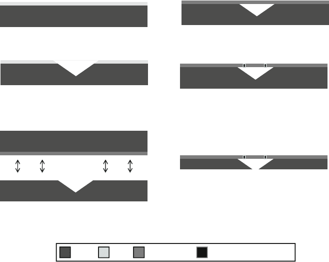
The process begins with the use of a standard thickness silicon wafer with <100>
orientation (Fig. 14.43). A thin-film layer is grown or deposited onto the surface of
the wafer followed by a photolithography and etch to expose square openings in the
masking layer. The wafer is then etched using an anisotropic wet chemical etchant
to form pyramidal pits in the surface of the wafer (Fig. 14.43b). This resultant shape
is due to the fact that the thickness of the wafer is nominally 525 µm and the mask-
ing openings are 250 µm, and therefore the anisotropic etchant self terminates on
the exposed <111> crystallographic planes resulting in an etch pit depth of approxi-
mately 175 µm. The masking layer is removed and then a second silicon wafer that
is p-type with an n-type epitaxial layer is directly bonded to the wafer having the
previously etched pyramids on the surface (Fig. 14.43c).
The thickness of the epitaxial silicon layer will set the thickness of the diaphragm
of the resultant pressure sensor. Subsequently, the bulk of the bonded top wafer is
(a) Starting wafer with masking layer on surface.
(b) Pattering of masking layer, followed by
anisotropic wet etching.
(c) Preparation of a wafer with a n-type epitaxial
layer grown on surface, followed by direct
bonding of the two wafers together.
(d) Removal of p-type silicon from bonded top
wafer to leave behind thin n-type epitaxial layer.
(e) Ion implantation into selected regions on
surface of thin diaphragm to make piezoresistors,
followed by the deposition, patterning and
etching of metal to form electrical connections to
the piezoresistive devices.
(f) The back of the bottom wafer is lapped and
polished to thin it thereby opening up the cavity
and exposing the backside of the pressure
sensitive diaphragm.
Silicon Oxide n-type epi layer Ion Implanted PiezoresistorsSilicon Oxide n-type epi layer Ion Implanted Piezoresistors
Fig. 14.43 Cross-section of the process technology for the NovaSensor pressure sensor
1106 M.A. Huff et al.
removed using a controlled-etch process thereby leaving only the bonded epitaxial
layer on the bottom wafer (Fig. 14.43d). Piezoresistors are then made in selected
regions on the silicon diaphragm using ion implantation (Fig. 14.43e). Metal is
deposited, patterned, and etched to form electrical connections to the piezoresistors
on the diaphragm. Next, the composite wafer is lapped and polished back to reduce
its thickness to about 140 µm thereby opening up the cavity from the backside of
the diaphragm (Fig. 14.43f).
14.8.2.9 Microelectronics Wafer-Bonded (Bulk) Accelerometer Process
(Ford Microelectronics)
A multitude of process sequences have been developed over the last 20 years to fab-
ricate accelerometers. In addition to surface micromachined process sequences, bulk
micromachined and mixed surface–bulk micromachined process sequences have
been developed. This section examines a mixed process technology developed by
Ford Microelectronics, Inc. (FMI). The process contains wafer-level encapsulation
that is a classic example of lateral electrical feedthroughs. The goals of this process
were to provide a wafer-level, hermetic encapsulation of a silicon accelerometer. At
the time of its development, it provided a technology that was robust to the stresses
of the plastic packaging process and thus allowed low-cost plastic packaging. It also
provided an inert environment (dry nitrogen, neon) that could be maintained for >15
years. The sensing principle is a torsional accelerometer where unequal masses are
formed over a central fulcrum. The side with the larger mass moves more under the
influence of acceleration, thus providing a net change in capacitance one side to the
other.
The FMI process is a three-wafer process that includes a Pyrex
R
intercon-
nect/electrode substrate, a silicon device wafer, and a silicon cap wafer [28].
Each of the three wafers includes shared unit process steps, but they can be
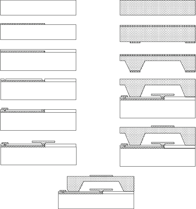
processed independently and in parallel. Starting with the 7740 Pyrex substrate,
the counterelectrodes and interconnects are a deposited metal stack comprised of
Cr/Au/Pt/Au/Cr (1500 Å), which is deposited by evaporation and patterned by liftoff
(see Fig. 14.44a). This thickness is acceptable for DC interconnection of the elec-
trostatic MEMS device. In the next steps, Pyrex is sputtered (1.5 µm) over the
interconnects to provide a semiplanarized bonding interface (Fig. 14.44b). It was
found for these metal and Pyrex film thicknesses that the surface was adequately
planarized to form a hermetic anodic bond. For thicker metal films necessary for
RF performance (0.5–1 µm or thicker), the sputtered Pyrex layer would need to
be thicker and a CMP process would need to be introduced. Following the sput-
tered Pyrex deposition, electrical vias are wet etched (Fig. 14.44c) and filled with
an evaporated Cr/Au/Pt contact metallization (Fig. 14.44d).
The device wafer process begins with a silicon wafer that has an n-epitaxial sili-
con (epi) layer, which is grown above a p+ etch-stop layer. The epi layer is etched in
two stages. First it is time-etched through part of its thickness leaving a protrusion
that will become the central fulcrum. Photoresist is applied a second time to form
the outline of the full structure. A further etch, which ends on the p+ etch stop layer,
forms the moving mass’s structure (Fig. 14.44f).
14 MEMS Process Integration 1107
(a) Glass Substrate
(b) Electrical Interconnect Deposit/Pattern
(c) Sputter deposit Pyrex insulator
(d) Wet etch electrical vias
(e) Deposit contact metal
(f) Anodic Bond Silicon Device to Glass
(l) Saw cut exposure of bond pad and sawin
g
of wafer, cuttin
g
Si and P
y
rex simultaneousl
y
(k) Pattern contact on silicon lid
(j) Anodic bond silicon lid to glass substrate
(h) Deposit and pattern silicon nitride mask
(g) Starting silicon wafer for lid
(i) KOH etch of 100
µm deep cavity
Fig. 14.44 Silicon micromachined wafer-bonded accelerometer and wafer-level encapsulation
process: (a) starting glass substrate, (b) deposition of metallization, (c) Pyrex deposition for pla-
narization, (d) etch to expose metallization for vias, (e) via deposition, (f) Pyrex wafer after the
bonding and dissolved wafer etch back of the device wafer to yield the accelerometer proof mass’s
fulcrum bonded to the metallization, (g) starting silicon lid wafer, (h) deposition of backside etch
mask, (i) backside KOH etch, (j) lid wafer bonded to the Pyrex wafer, (k) patterned lid metal-
lization, (l) final structure showing saw cut used to expose the bond pads on the Pyrex wafer
The silicon wafer and the Pyrex wafer are then anodically (i.e., electrostatically)
bonded together. The protruding central fulcrum contacts a metal pad on the glass
wafer allowing an electrical connection to the moving mass. In order to release the
moving mass, the n-“handle” portion of the wafer is completely etched away from
the backside in a type of dissolved-wafer process. In this case the backside etch
stops on the p+ layer. The p+ layer is then stripped leaving the structure shown in
Fig. 14.44f.
1108 M.A. Huff et al.
The third wafer is a silicon wafer ((100) n-silicon) used as the lid (Fig. 14.44g).
The first step deposits Si
x
N
y
on both sides of the wafer and patterns one side, such
that the Si
x
N
y
acts as a masking layer for a KOH etch (Fig. 14.44h). The KOH etches
a 100 µm deep cavity to provide a volume for the MEMS device and to provide
standoff height for the sawing process to expose the bond pads (Fig. 14.44i).
At this point the silicon wafer can be stored until it is needed for a mating wafer,
when the silicon nitride is stripped so the silicon wafer can be bonded to the Pyrex
wafer. One consideration with this stack is the thermal mismatch between the sili-
con wafer and the Pyrex wafer. The bonding process is performed with 300 V and
315
◦
C, where there is only a small difference in the CTEs of the two materials.
The silicon lid is shown bonded to the Pyrex wafer including the MEMS devices in
Fig. 14.44i.InFig.14.44j, a contact is deposited and patterned on top of the lid for
electrical connection via wire bond.
During the wafer sawing process, the first saw cuts partially saw through the
silicon wafer to expose the bond pads. With the bond pads exposed, a wafer-level
electrical test can be performed to identify known good die and verify functional-
ity. After the functional test, the sawing process is completed to singulate the die
(Fig. 14.44k).
14.8.2.10 Single-Crystal Reactive Etching and Metallization (SCREAM)
(Cornell University)
The SCREAM process was developed at Cornell University in the mid-1990s and is
used to implement high-aspect-ratio single-crystal silicon microstructures that have
metallized sidewalls [29]. It can be used for a variety of applications, but the primary
application has been for inertial sensors because the sidewall capacitance of the
high-aspect-ratio microstructures is relatively high compared to many other process
technology approaches. The SCREAM process technology uses only a single mask
thereby making it extremely simple and inexpensive. The low temperatures of the
SCREAM process also make it compatible with CMOS integration.
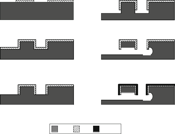
The process begins with a single-crystal silicon wafer that has a layer of silicon
dioxide grown or deposited on the top surface. The oxide layer varies between 1 and
2 µm in thickness. Photolithography is performed to pattern the oxide layer thereby
exposing the underlying silicon in certain regions (Fig. 14.45a). A deep reactive ion
etch is performed to a depth that depends on the structural height of the device, but
usually varies between 4 and 20 µm. Next, a layer of conformal silicon dioxide is
deposited by PECVD to a thickness of about 0.3 µm (Fig. 14.45b). A thinner oxide
layer may be used if a higher aspect ratio is desired. The purpose of this oxide layer
is to protect the top and sides of the structures made in the single crystal silicon
using DRIE in the previous processing step. The oxide is removed from the bottom
of the DRIE etched trenches using a RIE (Fig. 14.45c).
Another DRIE etch is performed to increase the depth of the trench into the
silicon wafer by about 3–5 µm (Fig. 14.45d). This purpose of this silicon etch is to
expose the silicon underneath the silicon structural elements. The silicon under the
structural elements is then removed to release them using an isotropic plasma silicon
14 MEMS Process Integration 1109
OxideSilicon Aluminum
(a).
Starting substrate is a single crystal silicon wafer.
An oxide layer is grown or deposited and then etched.
(b).
A DRIE is performed to etch trenches into the silicon
substrate and an oxide is then deposited using PECVD.
(c).
The oxide at the bottom of the trenches is removed
using RIE.
(d).
Another DRIE is performed to deepen the trenches
into the silicon wafer.
(e).
An isotropic silicon etch is performed to completely
release the silicon microstructures.
(g).
A thin layer of Aluminum is deposited to form
conductive electrodes on the structures.
Fig. 14.45 SCREAM process sequence
etch (either a plasma isotropic SF
6
etch or a xenon di-fluoride [XeF
2
]) as shown in
Fig. 14.45e. This etch chemistry is highly selective to the oxide masking layer that
is used to protect the silicon structural elements. A thin layer of aluminum having a
nominal thickness of 3000 Å is then sputter deposited onto the wafer (Fig. 14.45f).
The sputter deposition results in the metal coating the top of the structure as well
as the sides to form conductive electrodes that can be used for capacitive sensing or
electrostatic actuation. The devices are completed and the wafer can be diced and
packaged.
14.8.2.11 High-Aspect-Ratio Combined Poly and Single-Crystal Silicon
(HARPSS) MEMS Technology (University of Michigan and Georgia
Tech)
The HARPSS process technology was originally developed at the University of
Michigan [30] with further development performed at the Georgia Institute of
Technology. It enables the fabrication of microstructures from polysilicon and
single-crystal silicon having thicknesses varying from the tens to the hundreds of
microns as well as creating microstructures having extremely narrow gaps between
electrodes. The primary application of the HARPSS process technology has been
for inertial sensors (i.e., accelerometers and gyroscopes) wherein the large electrode
1110 M.A. Huff et al.
areas of the thick sidewalls combined with the narrow gaps allows very large capac-
itance values to be realized. The HARPSS process derives some of its attributes
from the hex–sil process technology wherein a mold made in silicon using DRIE
has a thin layer of oxide deposited on the sidewalls and the mold trenches are
filled with LPCVD polysilicon. Once the oxide is removed in HF, the polysilicon
microstructures are completely released and free to move [31].
The HARPSS process is a six-mask process technology and begins with a single-
crystal silicon wafer. A thin layer of silicon nitride (SiN) is deposited by LPCVD
to a thickness of 2000–2500 Å. The SiN layer is patterned and etched to serve as
an insulator between the bonding pads of the microstructure and the substrate. Deep
high-aspect-ratio trenches are then etched into the silicon substrate using DRIE to
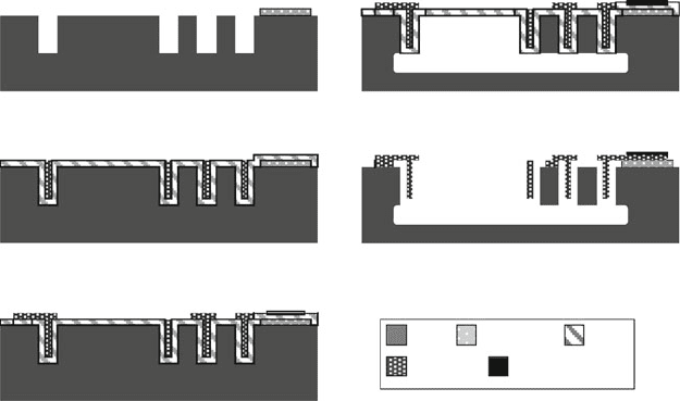
a depth of 50 to a few hundred microns (Fig. 14.46a). The depth of the trench etch
determines the height of the microstructures. Next, a highly conformal thin layer
of silicon dioxide is deposited using LPCVD (Fig. 14.46b). A conformal layer of
polysilicon is then deposited by LPCVD at 588
◦
Celsius to refill the oxide-coated
trenches etched into the silicon substrate. This layer of polysilicon will form a struc-
tural material layer for the devices made by this process and therefore must be doped
to increase its electrical conductivity. Boron doping is preferred over phosphorus
doping due to the slower etch rate of boron-doped polysilicon in HF during long
release etches. The doping of the polysilicon is performed by diffusion of boron
into the oxide trench coating layer prior to the polysilicon deposition. After the
polysilicon is deposited, a drive-in diffusion is performed to diffuse the boron from
the oxide into the polysilicon.
(a). Starting wafer is single crystal silicon wafer. A layer of SiN
is deposited, patterned and etched followed by a DRIE trench etch
into the silicon surface.
(b). A layer of oxide is deposited to conformally coat the trenches
and sidewalls. A layer of polysilicon is deposited to refill the
tenches. The Polysilicon on the surface is removed.
(c). The oxide is patterned and etched in selected regions on
the surface to open anchor areas for the subsequent polysilicon
deposition. Polysilicon is then deposited, patterned and etched.
A thin layer of chrome/gold is deposited, patterned and etched to
form electrical contact pads.
(d). A DRIE trench etch is performed, followed by a timed isotopic
etch to undercut the silicon microstructures in selected areas.
(e). A HF etch is performed to remove the oxide and thereby
release the microstructures.
Silicon Silicon Nitride Oxide
Polysilicon Metal
Fig. 14.46 HARPSS process sequence
14 MEMS Process Integration 1111
After the trenches have been refilled with polysilicon and the drive-in diffu-
sion has been performed, the polysilicon layer on the surface is patterned and
etched. The underlying oxide layer is also patterned and etched to open up areas
that act as anchor points for the microstructures. Another layer of polysilicon is
deposited, doped, patterned, and etched on the surface. A metal layer of chrome/gold
is deposited to a thickness of 3000 Å by evaporation and then patterned and etched
to form electrical bonding pads (Fig. 14.46c). A DRIE etching is performed into the
silicon substrate, followed by a timed dry isotropic SF
6
silicon etch to undercut the
silicon microstructures (Fig. 14.46d). Lastly, a HF etch is performed to remove the
oxide layer and thereby completely release the microstructures (Fig. 14.46e).
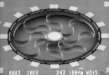
Figure 14.47 shows a SEM of a gyroscope fabricated using the HARPSS process
technology wherein exotically shaped structures such as the meandering supporting
tethers can be implemented rather easily.
Fig. 14.47 SEM of a
gyroscope fabricated using
the HARPSS process
technology. The
meandering-shaped
supporting tethers a re 80 µm
in height and 4 µmwide
(Reprinted with permission,
copyright Prof. Farrokh Ayazi
at the Georgia Institute of
Technology)
14.8.2.12 Hybrid MEMS (Infotonics)
There are many surface micromachining techniques such as the MUMPS and
Summit processes that use multilayer polysilicon as the main structural mate-
rials for MEMS devices. A few SOI process modules such as SOI MUMPS
(from MEMSCAP), aMEMS
TM
(from Teledyne, see also Section 14.8.2.18 in this
chapter), MigraGem (from Micralyne), and MEMSOI (from Tronics Microsystems)
processes have recently become available to create MEMS structures using the
single-crystal silicon (SCS) layer on SOI wafers [32–35]. There are a couple of
advantages of using the SCS layer as the MEMS structural material. First, compared
to polysilicon, SCS has excellent and reproducible mechanical properties such as a
high Young’s modulus, a repeatable Poisson ratio, and no residual stress or stress
gradients. Second, the conductivity of the SCS can be finely controlled over five
orders of magnitude. The SCS also has better optical properties such as lower opti-
cal loss in infrared range than other materials like polysilicon. However, SOI wafers
have only one SCS layer and it is difficult and costly to add more SCS layers later
in the fabrication to build a MEMS structure. The SOI process modules mentioned

1112 M.A. Huff et al.
above are based on only one SCS layer. Thus, there is a limitation on the variety of
MEMS devices that can be built by these SOI processes.
The hybrid MEMS process, initially developed at Xerox [36] and now available
at Infotonics Technology Center [37], can be used to create MEMS structures from
one polysilicon layer and one SCS layer on SOI wafers. Another hybrid process for
fabricating inchworm motors and hinged SOI legs using five masks has also been
developed at BSAC [38]. The advantage of the hybrid process is to combine the
flexibility of polysilicon processing and the unique material properties of SCS for
MEMS devices. Surface micromachining using polysilicon has been studied since
the 1980s and the process capability of polysilicon has been widely accepted. The
hybrid process can use the polysilicon as the mechanical support structures such
as dimples and anchors, and use SCS for the critical structures such as optical
waveguides. Compared to polysilicon surface micromachining, the challenges of
this process are twofold. First, SCS and the buried oxide (BOX) layer already exist
on the SOI wafer in the beginning. Many desired mechanical features such as dim-
ples and anchors have to be added to the existing SCS layer. Second, depending on
the thickness of the SCS layer, surface topography after patterning the SCS layer
can be greater than the typical polysilicon micromachining.
The complete hybrid process is a 13-mask integrated process including a 3 µm
polysilicon layer for static mechanical structures and anchoring, and a 5 µmSCS
layer to provide optimum mechanical and optical performance for optical MEMS
devices (waveguides and optical switches). Table 14.2 shows examples of MEMS
and MOEMS designs that can be fabricated using the entire process or the sub-
sets of the all-hybrid process. Because the optical devices are very sensitive to the
Table 14.2 Subsets of hybrid MEMS processes for different applications [37]
Mask names
Mask
number
Advanced
optical Waveguide
Rapid
optical
Rapid
mechanical
SCS shallow etch 1
√
SCS doping 2
√√
SCS anchor etch 3
√√
SCS dimple etch 4
√√
SCS gap fill
√
SCS precise cut 5
√√
SCS medium etch 6
√√
SCS final c ut 7
√√ √
TEOS and CMP
√
SCS expose 8
√
Silicon nitride 9
√
Polysilicon 10
√
TEOS etch 11
√
Bulk Si DRIE 12
Metal 13
√√
Totalmasks 84 26
Reprinted with permission, copyright 2005 IEEE
14 MEMS Process Integration 1113
lithography dimension and alignment accuracy, six masks are used to etch the pat-
tern on the SCS layer. Although extra masks increase the cost of the process, it
is sometimes necessary to achieve the desired design intent. The advanced optical
module, developed by the MOEMS Manufacturing Consortium, is an 8-mask subset
of this process [39]. Another example is waveguide devices such as AWG, which
is a 4-mask subset process [39]. An attractive feature of the Hybrid SOI Process
is that many subsets of the entire process can be used independently. Each subset
can carry a specific design function and can be made with a rapid turn-around time.
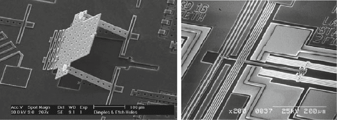
Figure 14.48 shows some examples of optical MEMS devices fabricated using the
hybrid MEMS process. The SCS layer was used to form an out-of-plane reflective
micromirror in Fig. 14.48a, and the optical waveguide switch and latching structures
using heat actuators is shown in Fig. 14.48b [37].
(a) (b)
Fig. 14.48 Optical MEMS devices fabricated using hybrid MEMS: (a) fixed reflective micromir-
ror; (b) optical waveguide switch with heat actuators [37] (Reprinted with permission, copyright
2005, IEEE)
The starting SOI wafers consist of a 5 µm thick SCS layer on top of a 1 µmBOX
layer. Figure 14.49 shows the schematic cross-section view of this process. The SCS
layer is etched 0.3 µm deep using the first mask (SCS shallow etch, Fig. 14.49a).
This etch is used to pattern the fiducial and functional structures such as optical
gratings. The second mask (SCS doping, Fig. 14.49b) is for phosphorus doping to
increase conductivity in the SCS layer. The doping in SCS will increase optical loss
and this mask can confine the doping to the desired electrically conductive areas.
The third mask (SCS anchor) and the fourth mask (SCS dimple, Fig. 14.49c
were used for DRIE on SCS. The anchor etch is completed through the entire BOX
to provide mechanical connection to the underlying wafer. The dimples are antis-
tiction structures and the dimple etch is only half-way through the BOX. A layer
of polysilicon is deposited to fill the anchor and dimple holes. Polysilicon is then
blanket-etched away to expose the SCS layer again ( Fig. 14.49d). The next mask
(SCS precision cut, Fig. 14.49e) is a high precision cut with all patterns under the
same dimension to avoid loading effect in dry etching. The sixth mask (SCS medium
etch, Fig. 14.49f) offers an intermediate SCS etch, that is, not all the way through to
