Ghodssi R., Lin P., MEMS Materials and Processes Handbook
Подождите немного. Документ загружается.

1084 M.A. Huff et al.
Current approaches for managing this impedance mismatch usually involve either
removing a large section of the wafer material from underneath the resonator struc-
ture or by using a suitably designed Bragg filter that reflects the acoustic energy of
the resonator away from the wafer substrate interface [4].
Currently, the FBARs manufactured and sold for commercial applications are not
integrated with microelectronics. This has to do with the economics of combining
a piezoelectric process that is strongly material parameter-dependent (e.g., the cou-
pling coefficient, frequency, and Q can significantly vary from required values by
the processing conditions) for the FBAR with a CMOS process that is highly parti-
cle defect-dependent (while still maintaining acceptable yield levels). Furthermore,
the economics of placing a few resonators per IC die where the die area used for the
resonators are large, makes the cost of integrated resonators prohibitive.
We review the process technology for the most successful FBAR device in the
marketplace, specifically the Avago Technology FBAR (original development began
under Hewlett-Packard Laboratories and then under Agilent Technologies). Avago’s
process technology uses MEMS fabrication techniques to create an air cavity under
the device to control the impedance mismatch on either side of the resonator that
would otherwise severely degrade the resonator’s performance.
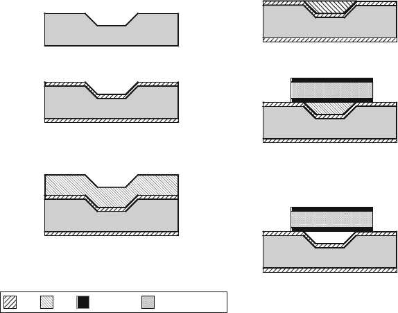
The process begins with a high-resistivity silicon wafer [7] ( See Fig. 14.16).
Photolithography is performed to define an area where a cavity is etched on the top
surface of the wafer. The resonator structure is fabricated so as to suspend across a
cavity or “swimming pool” etched into the silicon substrate. A cavity depth of a few
(a)
A shallow cavity is wet etched into the surface of the
silicon starting wafer.
(b) A thermal oxide is grown on the silicon wafer surface to
create a diffusion barrier to keep any dopants from the
sacrificial layer entering into the silicon substrate.
(c) A sacrificial layer of phosphorsilicate glass (PSG) is
deposited having approximately 8% phosphorous content.
(d)
Chemical-mechanical polishing (CMP) is performed on
the wafer surface, leaving only PSG material to fill the
cavity.
(e)
After cleaning, a thin layer of metal, such as Molybdenum
(Mo) is deposited which will be the FBAR bottom electrode.
Then a layer of Aluminum Nitride (AlN) piezoelectric
material is deposited. This is followed by depositing another
layer of Mo which will act as the FBAR top electrode.
(f)
The PSG sacrifical layer is removed from the cavity region to
release the resonator.
Molybdenum Aluminum Nitride
Silicon Wafer
PSGSiO
2
Silicon Wafer
Silicon Wafer
Silicon Wafer
Silicon Wafer
Silicon Wafer
Fig. 14.16 Cross-section of wafer through the Avago FBAR process sequence
14 MEMS Process Integration 1085
microns is sufficient. The cavity is formed in a high-resistivity wafer using conven-
tional dry etching techniques (Fig. 14.16a). The wafer is then thermally oxidized
to grow a thin layer of silicon dioxide (Fig. 14.16b). This silicon dioxide layer is
added to create a diffusion barrier against any dopants or contaminants from diffus-
ing into the silicon that would result in reducing its resistivity. This diffusion barrier
is needed in the Avago process because the subsequent step deposits a highly doped
glass onto the wafer surface. A layer of phosphorsilicate glass (PSG) having a thick-
ness more than the cavity depth is deposited at 450
◦
C using LPCVD ( Fig. 14.16c).
The phosphorous content of the PSG layer is approximately 8%. The PSG layer acts
as a sacrificial layer in the process sequence and is preferred due to its very high etch
rate in dilute hydrofluoric acid (HF). Moreover, the PSG is deposited at a relatively
low temperature, which limits the amount of phosphorous diffusion into the thermal
oxide diffusion barrier.
The surface of the as-deposited PSG layer is unsuited for deposition of the piezo-
electric device due to its relative roughness and therefore must be made smooth.
Specifically, a piezoelectric layer deposited on the as-deposited rough PSG layer
results in randomly oriented crystal growth and this material morphology exhibits
a highly reduced piezoelectric coefficient. A high-performance FBAR requires
that the piezoelectric device layer have a highly textured columnar crystal growth
wherein the crystals are perpendicular to the plane of the wafer. Also, the fabrication
process requires that the PSG layer be removed from the top surface of the wafer
and only remain within the etched cavity. Therefore, chemical-mechanical polishing
(CMP) is performed on the wafer top surface to remove the excess PSG and to make
the surface of the PSG atomically smooth (Fig. 14.16d). Subsequently, a thorough
cleaning is performed to remove any r esidual contaminants on the wafer surface that
may be left after the polishing process.
Next, a bottom electrode metal layer composed of molybdenum (Mo) or tungsten
(W) is deposited using sputter deposition. Although other metals may be used for the
FBAR electrodes, such as aluminum, gold, platinum, or titanium, the metal materi-
als Mo or W are preferred because of their low thermoelastic loss and high acoustic
impedance, which are important for creating a FBAR with a high Q and coupling
coefficient. Next, the piezoelectric layer is deposited which is composed of alu-
minum nitride (AlN) using sputter deposition. Then the top electrode is deposited
which is also a sputter deposited Mo (or W) layer. A thin mass loading step is
performed whereby a layer is patterned using liftoff to allow the frequency of the
shunt resonators to be lowered relative to the series resonators. This helps form the
half-ladder filter topology used in designing filters with steep skirts. This multilayer
stack is patterned and etched appropriately into the device structure and vias are
etched to expose the sacrificial PSG layer within the cavity under the FBAR device
structure (Fig. 14.16e). The wafer is then immersed into dilute hydrofluoric acid to
completely remove the PSG material from the cavity thereby completing the device
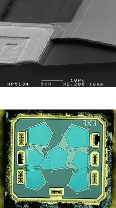
fabrication (Fig. 14.16f). Figure 14.17 is a SEM image of a completed FBAR device
that has been cross-sectioned.
In as much as a number of FBAR devices are usually fabricated onto a single die
each having different resonant frequencies (See Fig. 14.18), Avago has developed a
1086 M.A. Huff et al.
Fig. 14.17 SEM
cross-section of Avago FBAR
device (Reprinted with
permission, copyright Avago
Technologies, Inc.)
Fig. 14.18 Photograph of
Avago filter composed of a
number of FBARs made with
the Microcap process with the
silicon lid removed. The gold
ring around the perimeter and
each of the I/O connections
form a hermetic seal between
the individual resonators and
the outside environment
(Reprinted with permission,
copyright Avago
Technologies, Inc.)
number of methods for tuning the individual devices. These tuning methods involve
either adding (as in mass loading) or subtracting material from devices thereby mod-
ifying the device’s resonant frequency. These methods are described elsewhere [8].
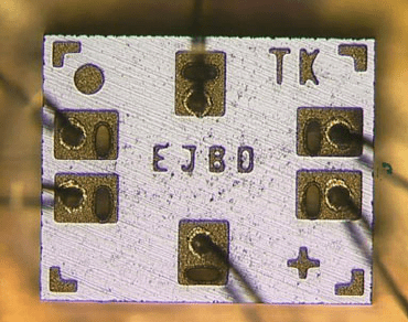
Also, the FBARs are encapsulated by bonding a silicon lid to the die as shown in
Fig. 14.19.
14.8.2.3 Summit V (Sandia)
Sandia National Laboratories has created a nonintegrated MEMS process technol-
ogy that is called Sandia Ultra-planar, Multi-level MEMS Technology 5, (SUMMiT
V
TM
)[9]. Of the nonintegrated process technologies that have been developed
in MEMS, SUMMiT V is perhaps the most sophisticated process technology
to date. It is a five-layer polysilicon surface micromachined process composed
14 MEMS Process Integration 1087
Fig. 14.19 A photograph of
a typical FBAR filter after
having been cap’d and
singulated. This shows the die
after wire bonding but, prior
to overmold (Reprinted with
permission, copyright Avago
Technologies, Inc.)
of one ground plane/electrical interconnect polysilicon layer and four mechani-
cal/structural polysilicon layers. The process sequence employs 14 photolithogra-
phy masks and makes use of chemical-mechanical polishing to maintain substrate
surface planarity as more mechanical/structural layers of polysilicon are added.
The SUMMiT V process has been successfully used for a diverse number of
applications. It was used to fabricate MEMS devices for space launch as part
of NASA’s Space Technology 5 (ST5) Micro-Sats program whose mission is to
explore concepts of building and operating miniaturized microsatellites. ST5 is the
first step in developing missions of tens or hundreds of small spacecraft that would
look at phenomena such as space weather. MEMS devices fabricated using the
Sandia SUMMiT
TM
V process were launched aboard NASA ST5 Micro-Sats, a
constellation of three microsatellites. Devices were ejected at 3-min intervals dur-
ing a launch aboard a Pegasus XL rocket on March 22, 2006. The spacecrafts’ orbit
is a “string of pearls”, in a near-Earth polar elliptical orbit that ranges from approx-
imately 300 (190 miles) to 4500 km (2800 miles) from the Earth. The SUMMiT
V process was also licensed to Fairchild Semiconductor who transferred the tech-
nology to a commercial foundry in Portland, Maine where it was used to produce
MEMS devices for several products in the marketplace. Sandia has been providing
access to the SUMMiT
TM
technology to the research and development community
through its SAMPLES prototyping program that supports small quantities of MEMS
devices.
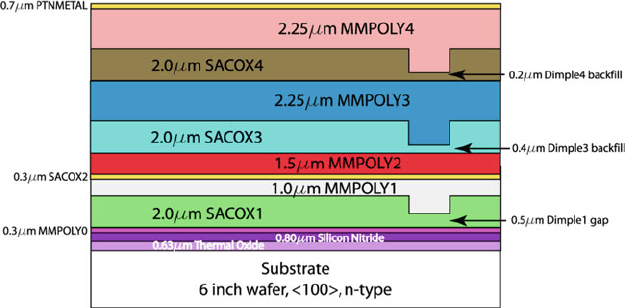
The Sandia SUMMiT V process starts with n-type <100> oriented 150 mm diam-
eter silicon wafers with a resistivity of 2–20 cm (Fig. 14.20). A thermal silicon
dioxide (SiO
2
) layer is grown on the wafers having a thickness of 0.63 µm. This
oxide layer serves as an electrical isolation. Next, a 0.80 µm thick layer of low-
stress silicon nitride (SiN
x
) is deposited to act as an etch stop layer. Photolithography
is performed (Mask 1, nitride-cut mask) on the substrates whereby the silicon
nitride and oxide layers are etched to create electrical contacts to the silicon sub-
strate. A 0.3 µm thick layer of doped polycrystalline silicon is deposited (poly0) by
LPCVD onto which photolithography is performed (Mask 2, mmpoly0 mask). The
1088 M.A. Huff et al.
Fig. 14.20 Cross-section of wafer processed using Sandia’s SUMMiT V process technology
showing the structural and sacrificial layers in the stack (Reprinted with permission, copyright
Sandia National Laboratories, SUMMiT
TM
Technologies, www.mems.sandia.gov)
poly0 polysilicon layer is etched using reactive ion etching (RIE) t o form areas for
mechanical anchors, ground planes, or electrical wiring interconnections. The first
sacrificial layer composed of silicon dioxide (SiO
2
) is deposited which is 2.0 µm
in thickness. Photolithography is performed (Mask 3, dimple-cut mask) on the sur-
face of the wafer to pattern the underlying oxide layer. Subsequently, the oxide is
etched using RIE to a depth of 1.5 µm; that is, the etch is not entirely through
the oxide layer. This partial etch of the oxide is used to form dimples, which are
essentially standoffs, in a mechanical/structural layer later deposited and etched in
the process sequence. A subsequent photolithography on the oxide layer is then
performed (Mask 4, sacox1-cut mask) and the oxide layer is etched using RIE com-
pletely through to the underlying polysilicon layer in the exposed areas to form
anchor sites.
A1.0µm thick layer of polycrystalline silicon (poly 1) is deposited by LPCVD
on the wafers, followed by another photolithography (Mask 5, mmpoly1 mask) and
etching using RIE to pattern the polysilicon layer into a mechanical/structural layer.
Photolithography is repeated on this layer (Mask 6, pin-joint-cut mask) and the layer
is completely etched using RIE to form hubs in the polysilicon layer for rotating ele-
ments. A layer of 0.3 µm thick silicon dioxide (SiO
2
) is deposited which is used in
the process as a second sacrificial layer or as a hard mask for mmpoly1 polysili-
con layer. Photolithography is performed (Mask 7, sacox2 mask) on this layer and
it is etched through its thickness using RIE. A 1.5 µm thick layer of doped poly-
crystalline silicon is deposited by LPCVD. Photolithography is performed (Mask 8,
mmpoly2 mask) and this layer is etched completely through using RIE. A 2.0 µm
thick layer of silicon dioxide is deposited using the TEOS process. This layer is the
third sacrificial layer of oxide in the process. Chemical-mechanical polishing is per-
formed on the top of the wafers to planarize the surface. Photolithography is then

14 MEMS Process Integration 1089
performed (Mask 9, dimple3-cut mask) on this layer followed by an etching using
RIE completely through the oxide layer. A 0.4 µm thick layer of silicon dioxide is
then deposited to backfill the dimple holes by LPCVD. Another photolithography
on this sacrificial layer is performed (Mask 10, sacox3-cut mask) and the exposed
oxide areas are completely etched through the layer using RIE to make anchors to
the underlying polyilicon layer.
Next, 2.25 µm of doped polycrystalline silicon (poly3) is deposited also by
LPCVD. Photolithography is then performed (Mask 11, mmpoly3 mask) on this
deposited polysilicon layer and the underlying polysilicon layer is then etched to
define the third mechanical/structural layer using RIE. A layer of silicon diox-
ide is then deposited that is 2.0 µm in thickness, which acts as a sacrificial layer
between the third and fourth polysilicon layers. This layer is the fourth sacrificial
layer of oxide in the process. Chemical-mechanical polishing is performed on the
top of the wafers to planarize the surface. Photolithography is performed (Mask 12,
dimple4-cut mask), followed by an etch using RIE completely through the layer.
A0.2µm thick layer of silicon dioxide is then deposited to backfill the dimple holes
between the third and fourth polysilicon (poly3 and poly4) layers. Photolithography
is repeated on this oxide layer (Mask 13, sacox4-cut mask), followed by a complete
etch through the layer using RIE to form openings between the third and fourth
polysilicon layers. A layer of polycrystalline silicon (poly4) of 2.25 µm thickness
is deposited by LPCVD which acts as the fourth and final mechanical/structural
layer. Photolithography is performed (Mask 14, mmpoly4 mask) on this layer and
the layer is completely etched through using RIE. A release etch is performed on
the substrates using a wet etchant solution composed of 100 to 1, HF and HCl, to
remove all exposed sacrificial oxide layers. Lastly, the substrates are dried using
either air evaporation (this only works if the micromachined structures are very
mechanically stiff), or supercritical dried using CO
2
(necessary for highly compli-
ant structures). Optionally, a layer of metal can be deposited to a thickness of 0.7 µm
and photolithography performed (Mask 15, ptnmetal-cut mask) to make electri-
cal contact to the topmost polysilicon mechanical/structural layer. Figure 14.21
Fig. 14.21 Cross-section of SUMMiT V wafer showing how the individual layers stack up and
features that can be realized in the process (Reprinted with permission, copyright Sandia National
Laboratories, SUMMiT
TM
Technologies, www.mems.sandia.gov)
1090 M.A. Huff et al.
illustrates more accurately how the layers stack up in the SUMMiT V process
sequence.
There are several interesting process integration issues involved in the SUMMiT
V process technology. First, there are no severe restrictions on thermal processing
because there are no electronic devices or metals involved (at least until the very end
of the process s equence). This allows LPCVD to be used for the multiple polysil-
icon and sacrificial oxide depositions. Moreover, high-temperature anneals which
are required in order to reduce the residual stress in the polysilicon layers can be
performed without degrading the other material layers.
Second, the totality of the polysilicon mechanical/structural layer thicknesses is
over 7.0 µm and the totality of the sacrificial oxide layers is over 6.3 µm, which
would result in an enormous topography of the wafer surface thereby severely
restricting the dimensions and type of devices that could be fabricated with this
process. The use of CMP to planarize the surface of the wafer after deposition of
the third and fourth sacrificial oxide layer depositions helps to solve this problem
and thereby allow higher levels of precision on the resultant device dimensions to
be obtained.
Third, the technique used to make the dimples in the first sacrificial oxide layer is
different from that used for either the third or fourth sacrificial layers. Specifically,
the dimples in the first sacrificial oxide layer are made using the standard technique
in surface micromachining of a timed partial etch through the entirety of the sac-
rificial oxide layer, whereas the dimples for the third and fourth sacrificial oxide
layers are made by an etch completely through the thickness of the sacrificial layer
followed by a deposition of oxide material to a thickness substantially less than that
of the oxide layer, thereby resulting in a dimple height equal to that of the sacrifi-
cial oxide thickness minus the thickness of the dimple backfill deposition thickness.
This technique for making dimples in the third and fourth sacrificial oxide layers is
needed due to the wide variation in the resultant thicknesses of the sacrificial oxide
layers after CMP is performed, thereby making it extremely difficult to control t he
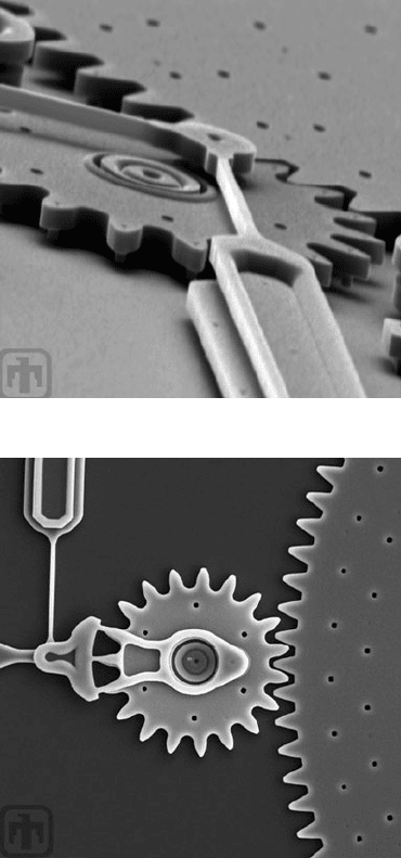
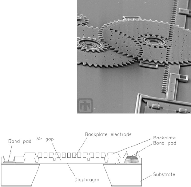
dimple height using a timed etch process. Figures 14.22, 14.23, and 14.24 are SEM
images of gear mechanisms made with this process, which demonstrate the level of
mechanical complexity that can be obtained with the SUMMiT
TM
V technology.
14.8.2.4 Microphone (Knowles)
The idea of constructing a MEMS-based acoustic transducer started quite early
in the evolution of MEMS devices [10–12]. However, it took many years before
the development of processes for commercial products began in earnest [12, 13].
The basic design requirement for a microphone is the construction of a low mass
diaphragm offset a short distance from a stiff backplate. Typically these structures
form the electrodes of a variable capacitance type microphone (although piezoresis-
tance and other pickoff mechanisms are possible). The combination of the flexible
diaphragm and the stiff backplate makes a variable capacitor whose capacitance is
a function of the diaphragm deflection. To reduce the damping of this system, the
backplate is generally perforated with holes.
14 MEMS Process Integration 1091
Fig. 14.22 A SEM of a gear
mechanism fabricated using
the Sandia SUMMiT V
process technology
(Reprinted with permission,
copyright Sandia National
Laboratories, SUMMiT
TM
Technologies, www.mems.
sandia.gov)
Fig. 14.23 ASEMof
another gear mechanism
fabricated using the Sandia
SUMMiT V process
technology (Reprinted with
permission, copyright Sandia
National Laboratories,
SUMMiT
TM
Technologies,
www.mems.sandia.gov)
The earliest commercially successful MEMS microphone process technology
was developed by Knowles, Inc. [14]. The Knowles 11-mask process technology
fabricates its diaphragm and its backplate on a single wafer (Fig. 14.25). The wafer
is KOH wet etched from the back side to expose the diaphragm and backplate. The
diaphragm, which is 1 µm thick polysilicon, is released such that it is a freely
floating plate. Thus, its stiffness is dependent on plate bending, requiring good
thickness control to obtain consistent device-to-device sensitivity. The backplate
is a 1.5 µm thick silicon-nitride layer, which is perforated to achieve the desired
damping. A conducting polysilicon layer is deposited on the diaphragm side of
1092 M.A. Huff et al.
Fig. 14.24 ASEMofan
overlaying gear mechanism
fabricated using the Sandia
SUMMiT V process
technology (Reprinted with
permission, copyright Sandia
National Laboratories,
SUMMiT
TM
Technologies,
www.mems.sandia.gov)
Fig. 14.25 Cross-sectional diagram of the Knowles, Inc. microphone sensor structure (Reprinted
with permission, copyright Knowles, Inc.)
the backplate and acts as the capacitive counterelectrode. Support posts of 4 µm
height are fabricated in the backplate to keep the diaphragm from collapsing into
the backplate due to electrostatic forces. The sensor is then assembled, along with
an associated readout ASIC, in an open cavity package.
Analog Devices developed a commercial MEMS microphone that has a similar
structure to the one described above. ADI’s microphone process is based on an SOI
process developed at the University of California at Berkeley [15]. The process was
first developed by ADI to fabricate optical MEMS and inertial sensors. In this orig-
inal process, the MEMS structures were constructed first by DRIE etching trenches
into the SOI layer and filling them with silicon dioxide and polysilicon. Circuits
were then constructed after the MEMS with a 0.6 µm double-polysilicon, double-
metal CMOS process. To convert this original process into a microphone process,
the DRIE etched silicon layer becomes the perforated backplane [16]. Then, a set of
spacer layers and a thin polysilicon diaphragm layer are added above the SOI layer.
An interesting feature of this process is that the sacrificial material that is etched
14 MEMS Process Integration 1093
Fig. 14.26 Top-down optical
micrograph of the Knowles,
Inc. microphone sensor
(Reprinted with permission,
copyright Knowles, Inc.)
Fig. 14.27 Sensor diagram
and SEM image showing the
backplane (BP), diaphragm,
and support posts (Post)
(Reprinted with permission,
copyright Knowles, Inc.)
Fig. 14.28 SEM image
showing backplane (upper
layer) with etch hole, support
post, and diaphragm (lower
layer) with small contact
dimple (Reprinted with
permission, copyright
Knowles, Inc.)
away to form the gap between the diaphragm and the backplate is also polysilicon.
The process must isolate the diaphragm polysilicon layer from the sacrificial polysil-
icon in order to etch away one and leave the other. Figure 14.32 shows an optical
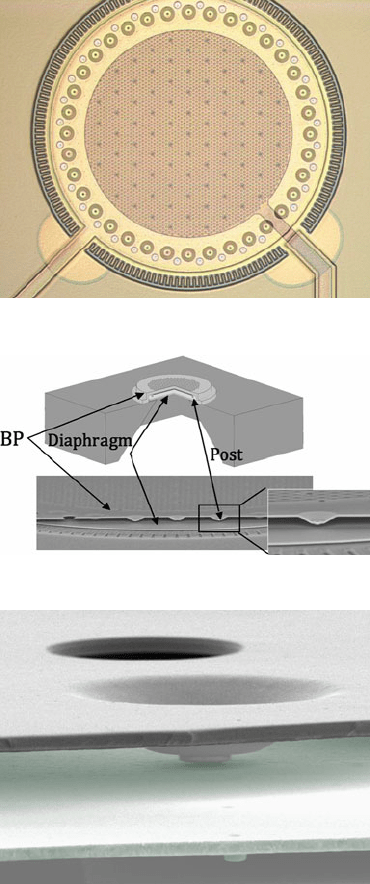
micrograph of the sensor structure. In addition to the backplate perforation pattern,
this image shows the 12 spring structures that support the polysilicon diaphragm.
