Ghodssi R., Lin P., MEMS Materials and Processes Handbook
Подождите немного. Документ загружается.

1094 M.A. Huff et al.
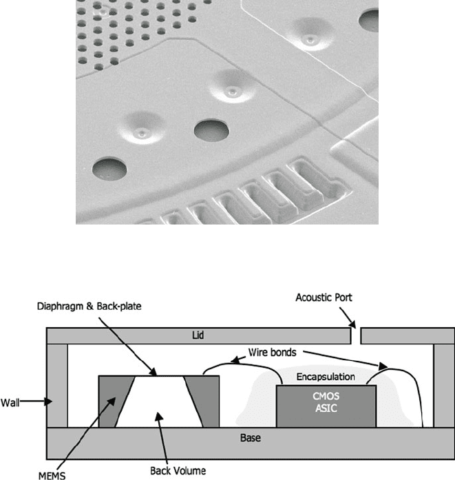
Fig. 14.29 SEM image of the backplate from above showing damping holes (small), support posts,
and etch holes (large) (Reprinted with permission, copyright Knowles, Inc.)
Fig. 14.30 Cross-section diagram of the MEMS microphone sensor and circuit ASIC in the open
cavity package (Reprinted with permission, copyright Knowles, Inc.)
14.8.2.5 Silicon Resonator (SiTime)
Quartz crystal oscillators are mechanical resonator devices that exploit the piezo-
electric effect in quartz material to create an electrical signal with an extremely
precise frequency. These devices are used in a number of timing applications includ-
ing quartz clocks and wristwatches, stable and precise clocks for most electronic
systems, digital integrated circuits and computers, and frequency stabilization for
communication systems. The market for quartz crystals is very large and is currently
estimated to be over 17 billion devices sold each year.
Recently, silicon MEMS-based oscillators have been developed and introduced
into the marketplace to compete with quartz oscillators. There are basically two
approaches: one is to have a discrete MEMS oscillator that is pin-for-pin compatible
14 MEMS Process Integration 1095
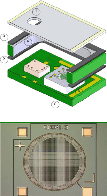
Fig. 14.31 Diagram showing
the assembly of the Knowles,
Inc. open cavity package
(Reprinted with permission,
copyright Knowles, Inc.)
Fig. 14.32 An optical image
of the ADI MEMS
microphone sensor
(Reprinted with permission,
copyright Analog Devices
Inc.)
with the quartz devices; and the other is to fully integrate the MEMS resonators
onto the CMOS as a monolithic solution. SiTime has introduced several devices
that take the first approach. Other companies have been developing fully integrated
devices, but because this approach requires modification to the CMOS fabrication
lines to make these devices, their introduction into the marketplace is expected to
take longer.
One of the key issues for implementing MEMS oscillators is how to make the
micromechanical resonator structure extremely stable. The SiTime solution is to
use a novel wafer-level packaging technology that is part of the resonator fabrica-
tion process whereby each resonator is encapsulated within a microcavity vacuum
chamber [17, 18].
The SiTime MEMS-based oscillator fabrication process begins with a 200 mm
diameter p-type silicon-on-insulator (SOI) wafer with a 10-µm thick silicon device
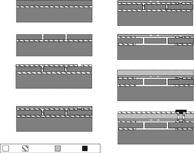
layer (Fig. 14.33a)[19]. Photolithography is performed to define the shape and
1096 M.A. Huff et al.
Starting wafer is 200 mm diameter SOI wafer with a
10 micron thick device layer.
DRIE is used to etch trenches through device layer.
Silicon dioxide is deposited using CVD to fill trenches
and planarize surface. The oxide is then etched to make
electrical contact to the silicon device layer.
Wafer is placed in an epitaxial reactor and a thin layer
of polysilicon is deposited over oxide layer.
The polysilicon layer is etched to make an array
of openings.
Vapor-phase HF is used to etch the oxide layer and
release the resonator structure.
A thick layer of polysilicon is deposited using
epitaxy to hermetically seal the resonator inside a cavity.
Vias to make electrical contact with resonator and
electrodes are made. Aluminum is deposited and
etched to make electrical interconnections and bond pads.
Silicon PolysiliconSilicon Dioxide Metal
(a)
(b)
(c)
(d)
(h)
(g)
(f)
(e)
Fig. 14.33 Cross-section of wafer processed using SiTime’s MEMS-based silicon oscillator
process technology
geometry of the silicon resonators, which are patterned by DRIE etching 0.4 µm
wide trenches completely through the silicon device layer (Fig. 14.33b). When the
process is complete, the silicon resonators will vibrate horizontally on the surface
of the wafer during operation.
A glass layer is deposited using CVD onto the surface of the wafer to a thickness
sufficient to completely fill the previously etched trenches made in the silicon device
layer and planarize the surface. Photolithography is performed, which is followed
by an etching process to create openings through the glass layer through which
electrical contacts will be made to the resonator and electrodes later in the pro-
cess (Fig. 14.33c). The glass from the field areas surrounding the resonators is also
removed. Next, the wafer is placed in an epitaxial silicon reactor wherein a layer
of silicon is deposited (Fig. 14.33d). The silicon deposited on the glass is polycrys-
talline, whereas the silicon deposited on the contact area in the glass is single-crystal
material. Photolithography is performed to define an array of openings through the
epideposited silicon layer at the location above the silicon resonator (Fig. 14.33e).
These openings will be used to remove the sacrificial oxide layer surrounding the
silicon resonator structure.
The wafer is placed in a vapor-phase hydrofluoric (HF) acid etch system and a
timed etch is performed to remove the oxide surrounding the silicon structure and
14 MEMS Process Integration 1097
thereby release the resonator (Fig. 14.33f). The resonator is now cleaned, sealed,
and encapsulated using the SiTime Epi-Seal
TM
process. This process is critical in
achieving a stable oscillator whereby the resonant frequency does not drift over
time or with subsequent packaging and soldering processing steps. The cleaning
process is performed in the epitaxial reactor at a temperature of over 1000
◦
C and
entails exposure of the wafer to a hot hydrogen and chlorine gas. This removes
all contaminants from the resonator structure. Subsequently, in the same epitaxial
reactor, a layer of polysilicon is deposited onto the surface of the wafer that seals
off the openings that were made through the first epitaxial silicon layer in order to
facilitate the release of the resonator (Fig. 14.33g).
At this point the resonators are sealed within a cavity that is at vacuum pressure.
A polishing process is performed on the surface, after which the surface appears
smooth and continuous. Photolithography is performed and the polysilicon is etched
to isolate the vias to the resonators and electrodes. The trenches are filled with glass
to planarize the surface. Contact holes are etched after contact photolithography.
Aluminum is deposited and patterned (photolithography is performed) and etched to
define metal electrical connections from the resonators and electrodes to bond pads.
A layer of silicon dioxide and silicon nitride is deposited to provide a protective
layer over the surface of the device (Fig. 14.33h). The resonators are diced, tested,
and packaged.
The SiTime approach encapsulates the resonator in a sealed cavity at the wafer
level and does so without consuming much space on the die. This approach pro-
vides a significant advantage on reducing packaging costs. However, because the
temperature of the sealing process is far too high for microelectronics, this approach
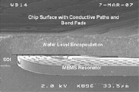
would not be suitable for an integrated MEMS resonator technology. Figure 14.34
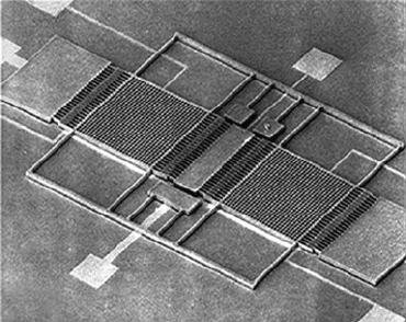
is a SEM of a SiTime MEMS device that has been cross-sectioned to display the
resonator within the wafer-level encapsulation.
Fig. 14.34 SEM of a SiTime MEMS device that has been cross-sectioned to display the resonator
within the wafer-level encapsulation (Reprinted with permission, copyright SiTime, Inc.)
1098 M.A. Huff et al.
14.8.2.6 Gyroscopes (Draper)
The Draper gyroscope is an example of a tuning fork gyro design whereby in-
plane electrostatic forces are used to excite the microstructure, and angular rates
are detected through the Coriolis forces which result in a differential out-of-plane
force loading on the two identical resonant proof masses. This differential force
causes the resonant proof masses to move relatively to one another and this move-
ment is capacitively sensed by electrodes located on the surface of the substrate
immediately underneath the resonant microstructures (Fig. 14.35). A derivative of
the Draper gyroscope process technology is now in commercial production.
Fig. 14.35 SEM of Draper
surface-micromachined
gyroscope fabricated with the
dissolved-wafer process
technology (Reprinted with
permission, copyright Charles
Stark Draper Laboratory,
Inc.)
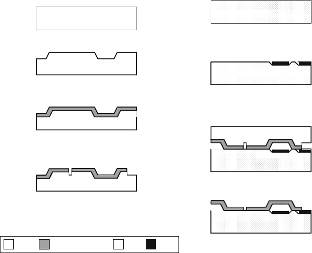
The “dissolved-wafer” process sequence (developed at the University of
Michigan) uses wafer bonding and high-aspect-ratio silicon surface micromachining
[20]. The process begins with an n-type silicon wafer that has a recess etched into
the surface using an anisotropic KOH etch (Fig. 14.36). This recess establishes the
gap spacing from the capacitive sense electrodes and the resonant microstructure.
Alternatively the gaps may be etched into the glass substrate wafer.
A deep boron diffusion is then performed to create a highly doped region in the
surface of the silicon wafer at a depth, which will determine the thickness of the
resonant microstructure, typically 5–20 µm (Fig. 14.36b). Alternatively, this layer
of highly doped silicon may be grown epitaxially on the surface of the silicon wafer.
After photolithography is performed to pattern the outline of the microstructure, a
RIE etch is performed through the highly boron-doped region of the silicon surface
and into the underlying lightly doped silicon substrate (Fig. 14.36c). This RIE etch
is best performed using a high aspect and deep silicon etch, such as DRIE.
A glass wafer that will be mated to the silicon wafer is prepared as follows. First,
a recess approximately 1600 Å is made into the surface of the Pyrex 7740 glass
wafer by wet etching. A multiple layer metal stack is then deposited, consisting
of 400 Å of titanium, 700 Å of platinum, and 1000 Å of gold. This metal stack is
patterned using liftoff thereby leaving the metal stack only in the recessed areas on
the glass surface (Fig. 14.36f). The multilayer metal stack is thicker than the glass
14 MEMS Process Integration 1099
Silicon Wafer
(a). Starting substrate is a n-type silicon wafer.
Silicon Wafer
(b). Wafer is masked in selected regions and exposed
silicon is time etched in KOH.
Silicon Wafer
(c). The surface of the wafer is heavily doped with
Boron using diffusion. Alternatively, this layer can
be created using an epitaxial silicon growth.
(d). RIE or DRIE is used to etch through the Boron-
doped layer of silicon and into the underlying silicon
substrate.
Glass Wafer
(e). A Pyrex 7740 glass wafer is used as the second
substrate in the process sequence.
Glass Wafer
(f). Recesses are etched into the Pyrex 7740 glass wafer
and a multiple layer stack of metal is deposited.
Silicon Wafer
Glass Wafer
(g). The silicon wafer is anodically bonded to the glass
wafer at 375 C and 1000 Volts.
Silicon Wafer
Glass Wafer
(h). The silicon wafer is removed by immersing the
bonded wafer pair in EDP which etches the lightly-doped
silicon but leaves the heavily boron-doped silicon.
Silicon Boron-Doped Silicon MetalGlass
Fig. 14.36 Process sequence for the Draper silicon tuning-fork gyroscope
recess, therefore the metal protrudes about 500 Å above the surface of the glass
wafer. This metal layer will form the capacitive sense electrodes and the output
electrical interconnects for the device.
The glass and silicon wafer surfaces are then aligned and anodically bonded to
one another using a temperature of 375
◦
C and an applied voltage potential of 1000 V
(Fig. 14.36g). Electrical contact to the silicon is made by overlapping the silicon rim
of the device over a small area of the metal on the glass wafer. The bonded wafer
is then placed into an ethylene–diamine–pyrocatechol (EDP) and water solution,
which is an effective etchant solution for silicon, but has excellent selectivity with
respect to the other materials used in the process sequence. The EDP etchant com-
pletely removes the silicon wafer but does not attack the highly boron-doped silicon
layer, which acts as an etch stop (Fig. 14.36h). The wafer is then ready for packaging.
14.8.2.7 Bulk Accelerometer (STMicroelectronics)
STMicroelectronics, Inc. has very quickly captured a significant portion of t he con-
sumer electronics MEMS sensor market by introducing a line of inertial sensing
devices that have excellent performance levels and are sold at extremely attrac-
tive prices, an absolutely essential requirement for most consumer applications.
STMicroelectronics refers to their microdevices development effort as a “MEMS
1100 M.A. Huff et al.
Epiphany,” which means that they claim t o have married the best that MEMS tech-
nology has to offer for enabling smaller, cheaper, higher performance, and more
functional devices (Technology Push) with a more innovative design approach
(Design Driven Innovation) resulting in MEMS devices that are better suited for
the consumer marketplace [21].
This strategy has been very successful and has allowed STMicroelectronics
to rapidly become the world’s largest producer of MEMS devices.
STMicroelectronics’ MEMS devices are currently used in such notable and
highly recognizable consumer products such as Nintendo’s Wii, Apple’s iPhones
and iTouch, and others [22]. For example, Nintendo’s Wii product employs
STMicroelectronics inertial sensors located in a handheld wand controller to s ense
the motion of a user who is playing tennis, golf, or any of the other available games
thereby allowing the user to be immersed and participate in the action on the screen.
This capability has radically advanced computer gaming from a purely passive
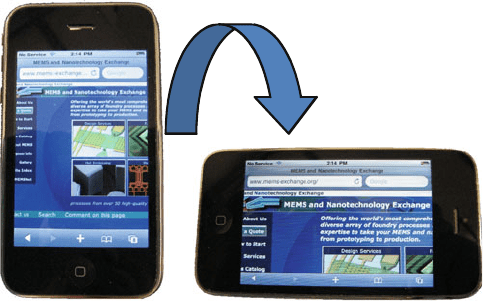
activity to a much more exciting fully active gaming endeavor. Similarly the Apple
iPhone uses STMicroelectronics MEMS sensors to detect the orientation of the
handheld communication device to the user’s perspective and adjusts the screen
display accordingly, thereby allowing much more user freedom and functionality
(Fig. 14.37).
Fig. 14.37 Photographs of products employing STMicroelectronics’ inertial MEMS sensor tech-
nology that provide the customer with radically new capabilities in consumer products (Reprinted
with permission, copyright MEMS and Nanotechnology Exchange)
The STMicroelectronics MEMS inertial products are based on their Thick
Epitaxial Layer for Microactuators and Accelerometers (THELMA) process tech-
nology as shown in Fig. 14.38 [23]. The THELMA process is a nonintegrated
MEMS process technology that is slightly more complex than a polysilicon sur-
face micromachining process technology, but has the distinct advantage of allowing
thicker structures to be implemented, which is extremely useful for capacitive-based
14 MEMS Process Integration 1101
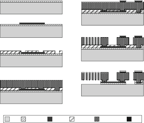
PolysiliconSilicon Epitaxial Polysilicon
(a) Starting silicon wafer with thermally grown oxide.
(b) A thin polysilicon layer is then deposited, patterned
and etched.
(c) A 1.6 micron thick PECVD oxide layer is deposited,
patterned and etched.
(d) A 15 micron thick epitaxial polysilicon layer is
deposited.
(f) The epitaxial polysilicon layer is patterned and etched.
(e) Metal is deposited, patterned and etched.
(g) The thick polysilicon structure is released using vapor HF.
Silicon Dioxide PECVD Oxide Metal
Fig. 14.38 STMicroelectronics’ THELMA process technology that is used to manufacture their
line of inertial sensors
inertial sensors. The THELMA process technology is used to implement capacitive-
based inertial devices, but is sufficiently flexible to be used for the production of
accelerometers, gyroscopes, and other MEMS device types.
The process begins with a silicon wafer onto which a 2.5 µm thick thermal silicon
dioxide layer is grown (Fig. 14.38a). Next, a polysilicon layer (poly1) is deposited
using LPCVD. This polysilicon layer is patterned and etched to form buried elec-
trical interconnections that are used as pathways for the potential and capacitive
signals from the device to the outside world (Fig. 14.38b). This layer can also be
used as a structural layer for thin polysilicon micromachined devices depending on
the device design as well. A 1.6 µm thick layer of silicon dioxide is then deposited
using PECVD. This PEVCD oxide layer in combination with the 2.5 µm thick ther-
mal oxide layer forms a composite 4.1 µ m thick layer of oxide that acts as the
sacrificial layer in the THELMA process technology. The deposited PECVD oxide
layer is then patterned and etched forming anchor regions for the thick polysilicon
devices that will be implemented later in the process (Fig. 14.38c). Next a thick layer
of polysilicon is deposited using epitaxial deposition (Fig. 14.38d). The thickness
of this layer can be tailored to the device design and can range from 15 to 50 µm.
A metal layer is deposited, patterned, and etched that is used to make electrical con-
nection to the sensor device (Fig. 14.38e). Subsequently, the thick polysilicon layer
is patterned and etched using deep reactive ion etching stopping on the underlying
1102 M.A. Huff et al.
oxide layer (Fig. 14.38f). The DRIE allows very high-aspect-ratio structures to be
made in the thick polysilicon layer. The sacrificial oxide layer is removed using
vapor hydrofluoric acid to release the structural polysilicon layer (Fig. 14.38g).
One of the key aspects of the STMicroelectronics inertial sensors is the low-
cost packaging approach that they have pioneered for high volume production. As
stated earlier, packaging of MEMS devices can often be the most expensive element
of the manufacturing process. The STMicroelectronics approach uses a glass frit
low-temperature wafer-scale bonding process to seal the inertial device within an
enclosed cavity between two wafers. This is followed by a land-grid array (LGA)
matrix platform packaging technology that they have pioneered for final assem-
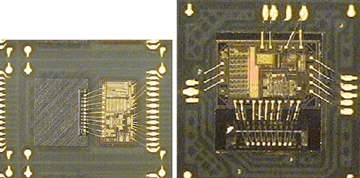
bly and packaging. In this process, the individual sensor die can be placed next to
the microelectronics die (the so-called side-by-side configuration) or the sensor and
microelectronics die can be placed on top of one another (the so-called stacked chip
approach) as shown in Fig. 14.39.
Fig. 14.39 Two configurations of STMicroelectronics’s inertial sensor packaging: (left) the side-
by-side configuration, and (right) the stacked chip approach (Reprinted with permission, copyright
STMicroelectronics, Inc.)
In the stacked chip configuration, the sensor die are first bonded to a large-area
substrate using an adhesive film (Fig. 14.40). Stacking of the microelectronics die
and the MEMS die onto each other enables the package to be kept very small
(Fig. 14.41). Wirebonding to the electrical pads on the die is performed and then
the die are encapsulated using an injection molding plastic process. This packaging
approach is performed on large-area substrates and is comparatively inexpensive.
Packaging stress, particularly stresses introduced by the adhesive bonding and
injection molding processes were significant challenges that STMicroelectronics
needed to develop suitable solutions for in order for this approach to be success-
ful. Figure 14.42 shows the evolution of STMicroelectronics device package for
their ultracompact linear accelerometer that is commonly used in many consumer
products.
14 MEMS Process Integration 1103
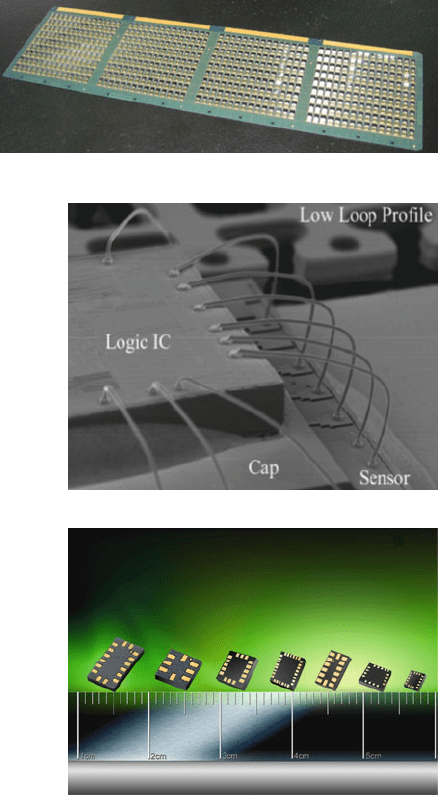
Fig. 14.40
STMicroelectronics’
approach to low-cost and
small profile packaging for
their MEMS inertial sensor
devices (Reprinted with
permission, copyright
STMicroelectronics, Inc.)
Fig. 14.41 A SEM showing
the stacking of the
microelectronics die on top of
the MEMS sensor die
followed by wirebonding and
prior to injection molding to
encapsulate the devices
(Reprinted with permission,
copyright
STMicroelectronics, Inc.)
Fig. 14.42 A photograph of
the evolution of the
STMicroelectronics inertial
sensor package (Reprinted
with permission, copyright
STMicroelectronics, Inc.)
14.8.2.8 Pressure Sensor (NovaSensor)
The pressure sensor was the first MEMS device of significant technological and
economic importance. These types of sensor devices continue to represent a large
and important part of the MEMS component industry with annual sales of well over
$1 B for an enormous diversity of applications including: automotive, aerospace,
industrial control, medical, environmental control, and so on. Essentially these
devices are composed of a thin diaphragm of material that is usually made of sili-
con that deflects under the application of a differential pressure loading across the
diaphragm. A number of schemes can be used for transduction of the diaphragm
