Ghodssi R., Lin P., MEMS Materials and Processes Handbook
Подождите немного. Документ загружается.

1114 M.A. Huff et al.
D
E
F
G
H
I
K
J
L
M
P
A
B
C
N
Single crystal silicon;
Silicon oxide;
Polysilicon;
Doped SCS;
Nitride;
Metal.
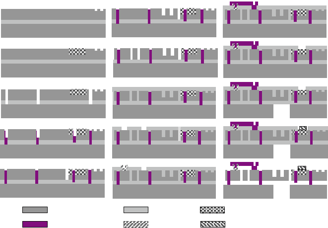
Fig. 14.49 Schematic cross-section view of fabrication process [37] (Reprinted with permission,
copyright 2005, IEEE)
the BOX. It is used to pattern structures such as rib waveguides and gratings within
the SCS layer. The last mask (#7) on the SCS layer (SCS final cut, Fig. 14.49g)
is another DRIE on SCS for actuator patterns, which removes large areas in SCS.
The pattern sizes can be in wide ranges and the loading effect can be eliminated by
overetching.
One of the key challenges for MEMS fabrication is to overcome the topog-
raphy created by DRIE on the SCS. After large areas of the SCS layer are
etched away, it is very difficult to use thin photoresist for photolithography. Thus,
8 µm LPCVD low-stress tetraethylorthosilicate (TEOS) oxide was deposited and
chemical-mechanical planarization was performed to minimize topography after
DRIE in the SCS layer. A few cycles of deposition and a blank etch process have
been developed to eliminate buried keyholes in the TEOS oxide layer. The thick
oxide layer is then planarized using CMP, which uses a silicon nitride layer under
the TEOS as a polishing stop. Hence, it is desired to select the slurry and pad for
high selectivity between the oxide and nitride. Another 2 µm of TEOS oxide is
deposited after CMP (Fig. 14.49h) as the sacrificial layer.
The eighth mask (SCS expose, Fig. 14.49i) opens up the 2 µm TEOS oxide.
A layer of silicon nitride is deposited and patterned (mask #9) to provide elec-
trical isolation (nitride, Fig. 14.49j). Mask #10 is for a 3 µm low-stress-doped
LPCVD polysilicon (polysilicon, Fig. 14.49k). This polysilicon layer is used for
static mechanical structures. Mask #11 (TEOS etch, Fig. 14.49l) is used to open
14 MEMS Process Integration 1115
areas in the TEOS oxide for metal contact. The underlying wafer can be etched
from the backside by DRIE using mask #12 (bulk Si etch, Fig. 14.49m). Metal such
as Cr/Au is deposited using liftoff techniques with mask #13 (metal, Fig. 14.49n).
The final release step can be a wet process (HF solution) or a dry process (HF vapor)
(Fig. 14.49p).
In summary, six masks are used for patterning the SCS layer including three dif-
ferent etching depths in the SCS layer (shallow, intermediate, and full). The various
etching steps enable designs such as optical gratings, channels, waveguides, and
actuators. Although it may cost more for extra masks, there are a few advantages:
(1) precise dimensional control (within ±0.2 µm error for optical devices), (2) dim-
ples on released SCS structures (preventing stiction), and (3) anchoring of the SCS
layer (for long release in HF). The mask for confining doping areas (mask #2)
avoids the large loss of optical signals in waveguides due to doping. Polysilicon fill
and TEOS oxide fill level the surface topography and enable the multilayer MEMS
structures.
14.8.2.13 Silicon-On-Glass (University of Michigan)
The silicon-on-glass (SOG) process was developed at the University of Michigan
[40] and has been used in applications requiring high-aspect-ratio and thick
single-crystal silicon structures. The applications and devices that the SOG pro-
cess has been used in include: inertial sensors (e.g., accelerators and gyroscopes
for automotive, medical, industrial, and aerospace applications), microactuators
(e.g., microvalves, micropumps, optical devices, comb drive actuator devices), and
micromechanical resonators (e.g., RF MEMS devices, communication devices,
optical devices), and several others.
The SOG process utilizes a relatively thick single-crystal silicon device layer
(100–150 µm in thickness) and a high-aspect-ratio etch process (up to 50 to 1 as
quoted as possible by the University of Michigan, but typically a 15 to 1 aspect ratio
is more common) to realize thick and high-aspect-ratio microstructures. A major
feature is that the single-crystal silicon layer is supported on an insulating glass
substrate thereby eliminating the expense and complexity of using SOI wafers. The
SOG process can be performed on standard microelectronic wafers (such as CMOS
wafers made through an IC foundry process) or die using postprocessing steps that
are compatible with microelectronics.
The SOG process starts with a 500 µm thick glass wafer, usually a borosili-
cate glass wafer such as Pyrex 7740 so as to have a thermal expansion coefficient
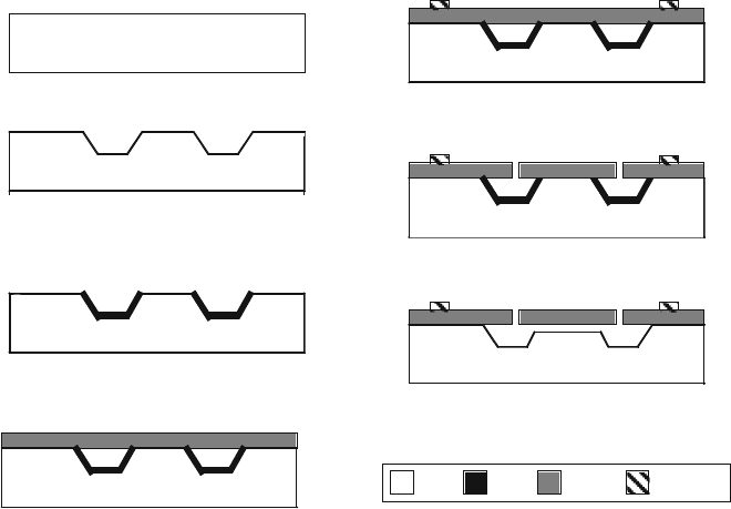
matched to that of silicon (Fig. 14.50). Photolithography is performed (mask level 1)
on the top surface of the glass wafer (and a protective photoresist is deposited on
the wafer backside) and subsequently the wafer is etched in a wet chemical etchant
solution (i.e., hydrofluoric acid) to form recesses approximately 10 µm in depth
(Fig. 14.50b). This etch is isotropic in nature and therefore the undercut of the glass
must be considered in the mask layout.
Typically, the first mask includes anchors that will be temporary and serve to
support the silicon device layer during fabrication. These anchors will be removed
1116 M.A. Huff et al.
Glass Substrate
Glass Substrate
(a). Starting substrate is a glass wafer having a
500 micron thickness.
(b). Photolithography (Mask Level 1) and etching
is performed to form recesses into the surface
of the glass substrate. The recesses in the glass
are 10 microns in depth.
(c). A layer of ITO is deposited and patterned
(Mask Level 2) to act as a metal shield for the
subsequent DRIE etching.
(d). The glass wafer is anodically bonded to a thin
silicon wafer.
(e). A 0.5 micron thick layer of aluminum is
deposited and patterned (Mask Level 3).
(f). Photolithography is performed (Mask Level 4)
followed by DRIE etching entirely through the
silicon layer.
(g). The exposed ITO layer is removed and the
device is released by removing the glass anchors.
Glass Substrate
Glass Substrate
Glass Substrate
Glass Substrate
Glass Substrate
Glass SiliconITO Aluminum
Fig. 14.50 Process sequence for the silicon-on-glass process
later in the process and have a 30 µm edge length dimension as drawn on the
first mask level. Next a layer of indium tin oxide (ITO) is deposited at a thick-
ness of 2000 Å. ITO is selected due to its properties of being both conductive and
transparent. The transparency is important to allow inspection of the wafer dur-
ing fabrication whereas the conductivity is important to prevent charge buildup on
the glass wafer surface that would seriously degrade the quality of the subsequent
DRIE processing steps used to define the silicon device layer. Photolithography is
performed (mask level 2) to define the pattern in the ITO layer that can be etched or
ion milled. Alternatively, liftoff can be used to pattern the ITO layer (Fig. 14.50c).
The glass wafer is then anodically bonded to a single-crystal silicon wafer having
a nominal thickness of 100–150 µm. The silicon wafer having this thickness is
extremely fragile and care must be exercised during handling to prevent yield loss.
Alternatively, the glass wafer can be bonded to a thicker silicon wafer, but at the
expense of having to thin down the silicon wafer using lapping and polishing. Also,
because glass wafers do not have total thickness variations comparable to those of
silicon wafers, the resultant silicon device layer using lapping and polishing to thin
the wafer back will likely be of variable thickness (Fig. 14.50d).
The anodic bonding is performed at a voltage potential of 1000 V and a tem-
perature of 350
◦
C. A layer of aluminum of thickness of 0.5 µm is deposited on
the silicon wafer surface. This metal layer will be used to make ohmic contact to
14 MEMS Process Integration 1117
the MEMS devices. Photolithography is performed (mask level 3) to define the alu-
minum layer which is subsequently etched using a wet chemical etchant solution
(Fig. 14.50e). Photolithography is performed (mask level 4) to define patterns to be
etched into the silicon device layer. The silicon layer is then etched using a high-
aspect silicon DRIE etch process all the way though the silicon layer and stopping
at the glass substrate (Fig. 14.50f ). The DRIE etch rate will vary depending on the
amount of exposed silicon as well as the range of feature sizes. In general, smaller
gaps etch considerably more slowly than large areas in DRIE and therefore a con-
siderable overetch may be required in order to complete the etch. The exposed ITO
layer is then removed using a wet etchant. Next, the glass anchors are removed using
a wet chemical HF solution (Fig. 14.50g). Lastly, the wafer is then diced into indi-
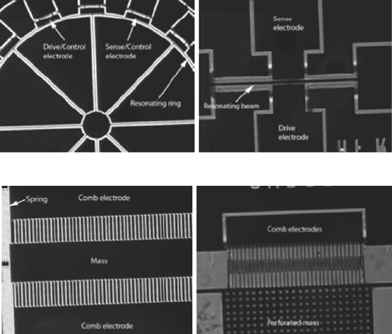
vidual die. Figure 14.51 shows the examples of different types of MEMS devices
made with the SOG process sequence. MEMS implemented with the SOG process
can be merged with microelectronics by flip-chip bonding of the CMOS die to the
exposed electrical pads made on the silicon device layer. However, the relatively
low doping (i.e., high resistance) of the silicon device layer must be considered in
selecting the CMOS process and device design.
(a) (b)
(c) (d)
Fig. 14.51 Example of MEMS devices made using the SOG process: (a) a vibrating ring gyro-
scope; (b) a beam resonator; (c) a perforated mass with comb electrodes; (d) an accelerometer
1118 M.A. Huff et al.
14.8.2.14 SOI MUMPS
TM
(MEMSCap)
The SOIMUMPS
TM
process is a simple double-sided etch and two-step metal pro-
cess that utilizes the predefined and fabricated layers found in silicon-on-insulator
starting material (Fig. 14.52a) rather than grown layers one sees in the other MUMPs
processes. By using this type of starting material, the process can be flexible enough
to offer multiple thicknesses of etched silicon using the same mask set.
(a). Starting SOI wafer.
(b). PSG deposition.
(c). A 20 nm thick layer of chrome
and 500 nm thick layer of gold, is
deposited and patterned through a
liftoff process.
(d). Photolith is performed and the
silicon layer is etched using DRIE.
(e). Frontside protective layer is
deposited and backside of wafer
is etched using DRIE.
(f). Wet oxide etch is performed
and then frontside protective layer
is removed.
(g). Shadow mask is used to
deposited a patterned layer of
50 nm of Chrome and 600 nm of
Gold.
(h). Shadow mask is removed.
Silicon Substrate Bottom Oxide Shadow Mask
Oxide Metal PSG (dopant) Frontside Protection Material
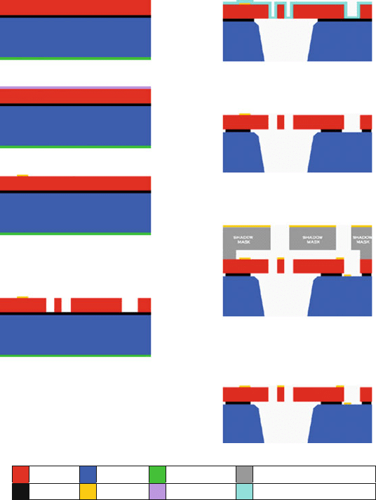
Fig. 14.52 MEMSCap’s SOIMUMPS process sequence. (a) Starting SOI wafer. (b) PSG deposi-
tion. (c) A 20 nm thick layer of chrome and 500 nm thick layer of gold, is deposited and patterned
through a liftoff process. (d) Photolith is performed and the silicon layer is etched using DRIE.
(e) Frontside protective layer is deposited and backside of wafer is etched using DRIE. (f)Wet
oxide etch is performed and then frontside protective layer is removed. (g) Shadow mask is used to
deposited a patterned layer of 50 nm of Chrome and 600 nm of Gold. (h) Shadow mask is removed
(Reprinted with permission, copyright MEMSCap, Inc.)
14 MEMS Process Integration 1119
The process begins with doping of the SOI device layer using PSG which is sub-
sequently stripped (Fig. 14.52b)[41]. The first metal layer, a metal stack of 20 nm
of chrome and 500 nm of gold, is patterned through a liftoff process (PADMETAL)
to define finer metal features for bond pads and routing lines (Fig. 14.52c). Because
this metal is exposed to high temperature during the subsequent process, sur-
face roughness tends to be higher and not suitable for low-loss optical mirror
applications.
Silicon is lithographically patterned with the second mask level (SOI), and etched
using deep RIE (Fig. 14.52d). This etch is performed using inductively coupled
plasma (ICP) technology; a special SOI recipe is used to virtually eliminate any
undercutting of the silicon layer when the etch reaches the buried oxide of the SOI
substrate.
A frontside protection material is applied to the top surface of the silicon layer
to protect frontside features from the rigors of the backside etch. The substrate
layer is lithographically patterned from the bottomside using the third mask level,
TRENCH. This pattern is then etched into the bottom side oxide layer using RIE.
DRIE is subsequently used to etch these features completely through the substrate
layer, allowing for through-hole structures (Fig. 14.52e). A wet oxide etch pro-
cess is then used to remove the buried oxide layer in the regions defined by the
TRENCH mask. The frontside protection material is then stripped in a dry etch pro-
cess which “releases” any mechanical structures in the silicon layer that are located
over through-holes defined in the substrate layer.
The r emaining “exposed” oxide layer is removed from the wafers using a vapor
HF process to minimize stiction. The exposed oxide layer is removed to allow
for electrical contact to the substrate and to provide an undercut in the oxide
layer that will prevent metal shorts between the silicon layer and the substrate
layer (Fig. 14.52f). The blanket metal layer, consisting of 50 nm Cr + 600 nm
Au, is deposited and patterned using a shadow masking technique (Fig. 14.52g).
The shadow mask is prepared from a separate double-sided polished silicon wafer.
Standoffs are incorporated into the side of the shadow mask that will contact the SOI
wafer, to avoid any contact with patterned features in the silicon layer. The shadow
mask is then patterned with the BLANKETMETAL mask, and through holes are
DRIE etched. The shadow mask is then aligned and temporarily bonded to the SOI
wafer, and the metal is evaporated using an e-beam tool. Metal is deposited on the
top surface of the silicon layer only in the through hole regions of the shadow mask.
After evaporation, the shadow mask is removed, leaving a patterned metal layer
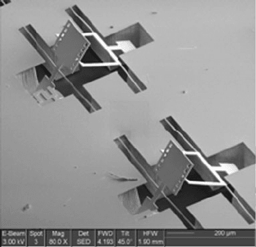
on the SOI wafer (Fig. 14.52h). Figure 14.53 is a SEM of some micromechanical
structures fabricated using the MEMSCap SOIMUMP
TM
process technology.
14.8.2.15 LIGA (CAMD, etc.)
LIGA is the German acronym for lithography, electroplating, and molding
(Lithographie, Galvanik, und Abformung) and is a very useful process technology
for making extremely high-aspect-ratio microstructures with high precision and
smooth sidewalls. The LIGA process was developed in the late 1970s at the
1120 M.A. Huff et al.
Fig. 14.53 SEM of some
devices fabricated using
MEMSCap’s SOIMUMPS
TM
process sequence (Reprinted
with permission, copyright
MEMSCap, Inc.)
Institut für Kernverfahrenstechnik (IKVT), today the Institute for Microstructure
Technology (IMT) in the Forschungszentrum Karlsruhe GmbH [42–44]. Several
institutes now use the LIGA process for developing prototype structures and com-
ponents often in collaboration with industry [45]. The benefits of LIGA principally
derive from the use of deep X-ray lithography. Although LIGA-made parts are rela-
tively demanding to fabricate, the technology is well suited for massive inexpensive
replication whereby the first-made part is used as a metal mold insert for hot emboss-
ing or injection-molding replication of the pattern into another material. Some of
the features and advantages of the LIGA process include: providing a large lay-
out freedom for the mask geometry; high aspect ratios of 20 to 1 are typical and
extreme ratios up to and beyond 100 to 1 have also been achieved; the s idewalls of
the structures made with the process are extremely parallel and have nearly verti-
cal sidewall angles (e.g., typical deviation of sidewalls is about 1 µm for structures
1 mm in height); the sidewalls of the LIGA structures are very smooth with R
a
val-
ues ranging from a few 10 nm to about 200 nm suitable for optical micromirror
surfaces; the precision in the lateral directions of LIGA-made structures is only a
few micrometers even over distances of several centimeters; and, it is also possi-
ble to create multilevel structures using a double exposure process [46]aswellas
different sidewall angles by tilting and rotating the sample during exposure [47].
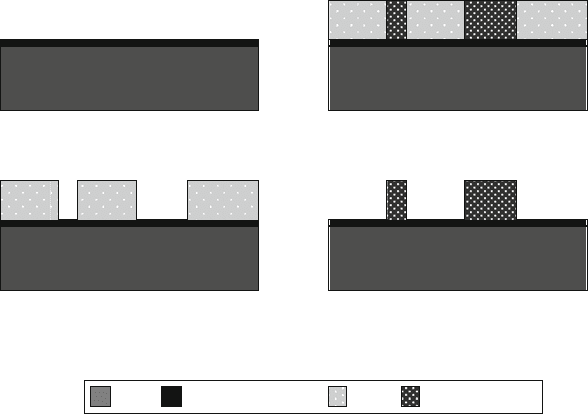
The complete LIGA process technology involves several main fabrication steps
that are described below and illustrated in Fig. 14.54. The fabrication begins with
the making of a suitable X-ray mask, which is typically composed of a thick gold
layer patterned using optical lithography (not shown) [49]. The patterned gold layer
will act as an absorber layer for the subsequent X-ray exposure. The X-ray mask
is used to expose a thick resist layer on a substrate material (usually Si) that is
composed of polymethylmethacrylate (PMMA) at a thickness ranging from a few
10 µm up to 3 mm. The PMMA layer is exposed on the substrate using deep X-ray
lithography (Fig. 14.54b). The substrate will have a plating seed layer, typically a
14 MEMS Process Integration 1121
(a). Starting wafer (typically a silicon wafer) has a metal
plating seed layer deposited on the surface.
(b). A thick layer of PMMA, typically ranging in thickness
between 100 um and 3 mm is cast onto the wafer and then
exposed by x-ray and subsequently developed into a plating
mold.
(c). Electro-plating is performed of Nickel, Gold or Copper on
the wafer surface and into the mold made of PMMA.
(d). The PMMA mold layer is removed thereby releasing the
high-aspect ratio metal microstructures.
Silicon
Plating Seed Metal Layer
PMMA
Electro-Plated Metal
Fig. 14.54 Illustration of t he basic LIGA process
titanium layer with a wet chemically etched TiO
2
layer deposited onto its surface
prior to the deposition of the PMMA layer (Fig. 14.54a). High-energy X-ray photons
are used for this exposure, therefore the developed resist pattern will have extremely
smooth and nearly vertical sidewalls. Within the newly created high-aspect-ratio
resist mold, a metal, such as gold, copper, or nickel, is electroplated into the features
thereby forming metal structures having the dimensions and form factor, but reverse
polarity, of the resist mold (Fig. 14.54c). The resist is then removed to release the
metal high-aspect-ratio microstructures (Fig. 14.54d). A sacrificial layer may be
made on the surface of the plating seed layer to create overhanging microstructures
[11]. Optionally, the LIGA-made metal microstructure can be used as a tool insert
for a hot embossing process to replicate the features into a polymer material. The
polymer parts may be the final parts, or they may be used as molds for electroplating
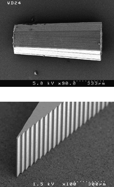
metal to replicate metal parts (also not shown) [50]. Figures 14.55 and 14.56 are
SEM images of some structures made with the LIGA process sequence.
14.8.2.16 RF Switch (MEMStronics)
MEMS radio frequency (RF) switches have become of increasing interest for several
military and commercial applications due to their low cost and high performance
[51]. Most of the MEMS RF switches employ an electrostatically actuated movable
electrode that is activated by a voltage potential placed across the movable electrode
and a fixed counterelectrode. At a sufficiently high voltage, the electrostatic forces
overcome the mechanical stiffness of the movable electrode and make contact with a
fixed counterelectrode to close the switch. When the actuation potential is removed,
1122 M.A. Huff et al.
Fig. 14.55 SU-8 posts with
slanted sidewalls, ∼1mm
tall, ∼350 µm diameter made
by tilt-and-rotate X-ray
lithography fabrication
methods [8]
Fig. 14.56 SEM of a
high-aspect-ratio grating
structure (500 µm tall) with
smallest step heights of about
20 µm m ade from PMMA
using X-ray lithography at the
CAMD wiggler source [9]
the mechanical stiffness of the movable electrode restores it to its open-state posi-
tion. These devices possess several inherent advantages compared to competitive
technologies such as FETs or p-i-n diode switches. First, the resistive losses are
much lower because the MEMS switches are implemented from materials that have
a very high conductance at microwave frequencies. This is compared to the much
larger resistance levels associated with ohmic contacts of semiconductor-based
switches. Second, the MEMS RF switches have nearly perfect I–V linearity which
greatly improves their distortion characteristics and power handling as compared
to semiconductor-based switches which inherently possess nonlinear I–V behavior.
This enables MEMS RF switches to exhibit virtually no detectable harmonics or
intermodulation distortion. Third, the electrostatic operation of MEMS RF switches
requires negligible current consumption, in either the “on” or “off” states. The main
disadvantage of MEMS RF switches is their switching speed, which is typically a
few microseconds. Therefore, although MEMS RF switches are unsuited for some
applications such as transmit and receive switching, they are highly attractive for
applications involving electronic beam steering and forming, such as phased-array
antennas.
14 MEMS Process Integration 1123
There are several MEMS RF switches that have been recently introduced into
the market. One example is from MEMtronics, a technology that originally was
developed at Texas Instruments and then Raytheon Systems. The MEMtronics pro-
cess technology is reviewed here, but it should be noted that there are not enormous
differences between it and the other MEMS RF process technologies.
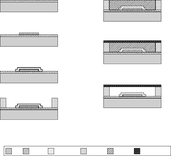
The process begins with a high resistivity (>5000 cm) silicon wafer
(Fig. 14.57)[52]. A thermal silicon dioxide layer is grown on the substrate sur-
face having a thickness of 1 µm. This layer will act as an insulator layer between
the metal conduction lines and the silicon wafer. Next, a layer of tungsten having a
thickness of 0.5 µm is sputter deposited and then patterned and etched to define the
switch electrodes (Fig. 14.57b). Subsequently, a layer of silicon nitride is deposited
by PECVD having a nominal thickness of 2000 Å. This layer is patterned and etched
to insulate the electrodes (Fig. 14.57c). The dielectric constant of the SiN film is
controlled to be nominally 6.7.
Next, a relatively thick layer of aluminum is deposited by evaporation for a total
thickness of 4 µm. This layer is then patterned and etched using a wet aluminum
etch solution to define the transmission lines and the standoff posts for the top elec-
trode (Fig. 14.57d). Due to the thickness of the aluminum layer combined with the
isotropic nature of wet etching, the dimension on the aluminum mask needs to be
(a)
Starting wafer is high resistivity (> 5000 ohm-cm)
silicon wafer. A 1 micron thick thermal oxide is
grown on the surface.
(b)
A 0.5 micron thick layer of Tungsten is deposited,
patterned and etched to define the bottom switch
electrode.
(c )
A 2000Ang. thick layer of silicon nitride is
deposited by PECVD, patterned and etched.
(d)
A 4 micron thick layer of Aluminum is deposited
using evaporation and then patterned and etched to
form the transmission lines and the standoffs for the
switch top electrode.
(e)
A photoresist layer is spin coated onto the wafer and
patterned. This layer acts as the sacrificial layer in
the process sequence.
(f)
An aluminum-alloy layer is sputter deposited and
then patterned and etched into the shape of the top
electrode.
(g)
The wafer is placed into an oxygen plasma to
remove the photoresist sacrificial layer.
AluminumSilicon NitrideTungstenSiO
2
Silicon Wafer
Silicon Wafer
Silicon Wafer
Silicon Wafer
Silicon Wafer
Silicon Wafer
Silicon Wafer
Photoresist Aluminum-Alloy
Fig. 14.57 Cross-section of the MEMStronics RF MEMS switch process technology
