Ghodssi R., Lin P., MEMS Materials and Processes Handbook
Подождите немного. Документ загружается.

1124 M.A. Huff et al.
oversized by approximately 5 µm to compensate for the lateral etch of the alu-
minum. A photoresist layer that is relatively thick is spin coated onto the wafer
and this layer will act as the sacrificial layer in the process sequence (Fig. 14.57e).
Once the photoresist layer has been patterned, an aluminum alloy layer is sputter
deposited and then patterned and etched into the shape of the switch top electrode
(Fig. 14.57f ). The sacrificial layer is then removed by placing the wafer into an oxy-
gen plasma thereby releasing the switch (Fig. 14.57g). Small openings (i.e., vias)
made in the top electrode metal layer allow the release etch time to be dramatically
reduced.
14.8.2.17 MetalMUMPS
TM
(MEMSCap)
The MetalMUMPS
TM
process was developed by MEMSCAP. The process involves
the electroplating of nickel to implement micromachined MEMS structures and has
been used successfully to fabricate microrelays based on thermal actuator technol-
ogy. The process features include: a nickel primary structural material layer that
can also be used as an electrical interconnect layer, a doped polysilicon layer that
can be used to make resistors or mechanical elements as well as cross-over inter-
connects for electrical routing, a silicon nitride electrical isolation layer, and a gold
overplating layer that provides for low contact resistance.
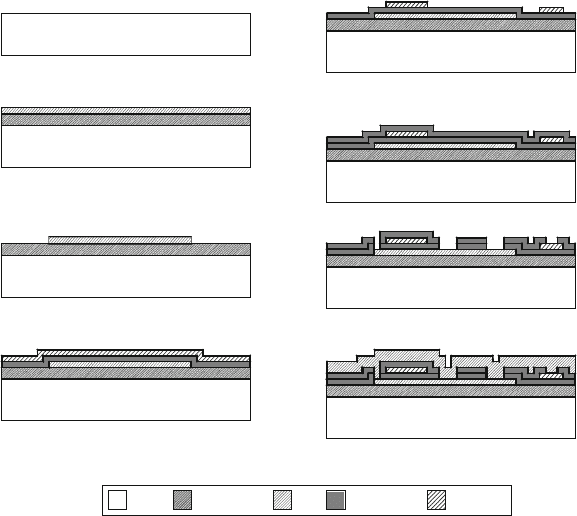
The process begins with an n-type single-crystal silicon wafer with (100) ori-
entation and a high resistivity (more than 4000 cm) (Fig. 14.58a)[53]. A 2 µm
thick layer of thermal oxide is grown on the wafer surface to provide electrical iso-
lation on the surface, followed by a 0.5 µm thick layer of PSG deposited using
LPCVD (Fig. 14.58b). This PSG layer (Oxide1) will act as a sacrificial layer to
release the Nitride1 layer and define the trench at the end of the process sequence.
Photolithography is then performed on the wafer surface to pattern the Oxide1 layer
(mask level OXIDE1). To define the PSG layer features, a wet KOH etch is used
that etches at a much higher rate than thermal oxide (Fig. 14.58c). After strip-
ping the photoresist, a 0.35 µm thick layer of low-stress silicon nitride (Nitride1)
and a 0.7 µm thick layer of polysilicon are deposited on t he wafer using LPCVD
(Fig. 14.58d). The polysilicon is doped using ion implantation and annealed to
make it electrically conducting. Photolithography is performed (POLY) to pattern
the polysilicon using RIE (Fig. 14.58e). After stripping the photoresist, a second
layer of low-stress silicon nitride having a thickness of 0.35 µm is deposited by
LPCVD (Fig. 14.58f). Photolithography is performed (NITRHOLE) to pattern both
the first and second silicon nitride layers using RIE (Fig. 14.58g). The nitride layers
serve several purposes: they provide a protective encapsulation for the polysilicon,
they define a protective layer on the substrate that determines where Si trench etch-
ing occurs later in the process, and a released and patterned nitride area may also be
used to provide a mechanical linkage between released metal structures that must
be electrically isolated.
After stripping of the photoresist, a 1.1 µm thick layer of PSG (Oxide2) is
deposited and annealed, but not released until the end of the process to free the
metal mechanical layer (Fig. 14.58h). Photolithography is performed (METANCH)
14 MEMS Process Integration 1125
(a). Starting wafer is a (100) oriented n-type single-crystal
silicon wafer.
Silicon Wafer
(b). A 2 micron thick layer of silicon dioxide is grown, followed
by the deposition of a 0.5 micron thick layer of PSG by LPCVD.
Silicon Wafer
(c). Photolithography is performed (Mask Level 1) and the PSG
layer is subsequently wet etched.
Silicon Wafer
(d). A 0.35 micron thick layer of silicon nitride is deposited,
followed by a 0.7 micron thick layer of polysilicon. Both layers
are deposited using LPCVD.
Silicon Wafer
(e). Photolithography is performed (Mask Level 2) to pattern the polysilicon
layer which is then subsequently etched using RIE.
(f). A 0.35 micron thick layer of silicon nitride is deposited by LPCVD.
Silicon Wafer
Silicon Wafer
(g). A photolithography is performed (Mask Level 3) to pattern the top and
bottom silicon nitride layers which are etched using RIE.
Silicon Wafer
(h). A 1.1 micron thick layer of PSG is deposited by LPCVD and the wafers
are then annealed at 1050 C for 1 hour.
Silicon Wafer
Silicon Thermal Oxide PSG Silicon Nitride Polysilicon
Fig. 14.58 First half of MEMSCap’s MetalMUMPS process sequence
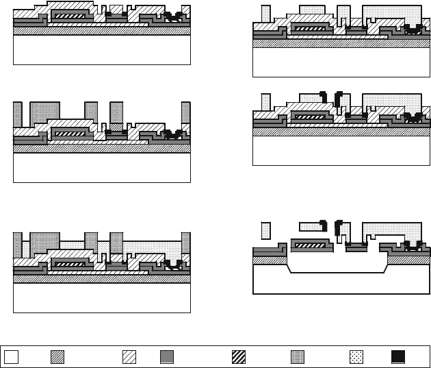
to pattern the PSG layer and the features are wet etched but the photoresist is left
on the wafers and a stack of 10 nm of chrome and a 25 nm layer of platinum is
deposited using evaporation. The metal is patterned using liftoff and remains only
in the areas where the PSG layer was removed in the METANCH mask level pro-
cessing, namely the bottom of the Oxide2 anchors which defines the metal structure
anchors (Fig. 14.59a).
A plating base layer composed of a 500 nm thick layer of copper followed by
a 50 nm thick layer of titanium is deposited to provide electrical continuity across
the wafer surface during the subsequent electroplating process. The final two mask
levels are for defining the thick metal features. The METAL mask level is patterned
using a thick resist to form the stencil for the electroplated metal layer (Fig. 14.59b).
A20µm thick layer of nickel is electroplated into the patterned resist (Fig. 14.59c).
Subsequently a 0.5 µm gold layer is plated on top of the nickel to provide a suitable
pad material for wire bonding of external electrical connections. This combination
of 20 µm nickel and 0.5 µm gold forms the metal layer, which serves as the primary
mechanical layer and electrical interconnect layer (Fig. 14.59d).
A final plated metal layer, sidewall metal, is a 1–3 µm gold layer plated on
selected areas of the sidewall of the metal layer to provide a highly reliable, low-
resistance electrical contact while also shrinking the gaps in adjacent electroplated
nickel structures. This unique process sequence uses the same feature designs twice
1126 M.A. Huff et al.
(a). Photolithography is performed (Mask Level 4) and the PSG layer is wet
etched. A thin layer of metal (10 nm of Chrome and 25 nm of Platinum) is
then deposited and patterned using lift-off.
Silicon Wafer
(b). A plating base composed of 500 nm of Copper and 50 nm of Titanium is
deposited (Not shown). The wafers are then coated with a thick photoresist and
photolithography is performed (Mask Level 5) to form the plating mold on the
wafer surface.
Silicon Wafer
(c). Nickel is plated on the surface of 20 microns and a Gold layer 0.5
micron thick is then deposited (Not shown).
Silicon Wafer
(d). The photoresist plating mold is then removed.
Silicon Wafer
(e). Two photolithography steps are performed. One using a bloated
mask (Mask Level 6) to remove the plating base from where sidewall
metal is desired and the second (Mask Level 7) to define a plating mold
for the Gold sidewall metal. A layer of Gold 1 to 3 microns in thickness
is then deposited and the photoresist mold is removed.
Silicon Wafer
(f). Plating base in exposed regions is stripped. Next the PSG sacrificial
layers are removed as well as the thermal oxide in the exposed regions.
The wafer is then etched in KOH to create trenches in the regions where
the silicon on the surface is exposed.
Silicon Wafer
Silicon Thermal Oxide PSG Silicon Nitride Polysilicon Photoresist Nickel Gold
Fig. 14.59 Second half of MEMSCap’s MetalMUMPS process sequence
(GOLDOVP) by “fattening up” the features on the first mask and using the as-
designed feature sizes on the second mask. The first exposure opens up an oversized
or “bloated” area in the thick photoresist layer where sidewall metal is needed fol-
lowed by the “unbloated” version of GOLDOVP for the desired resist pattern for the
actual sidewall metal. The 1–3 µm thick gold sidewall metal layer is then electro-
plated (Fig. 14.59e). The final steps are the release and Si trench etch. The release is
a series of wet chemical etches to first remove the plating base and then the sac-
rificial layers and the isolation oxide layer over the trench areas. Finally, a wet
chemical etch of the silicon, using KOH, is used to form a 25 µm deep trench in the
silicon substrate. This occurs in the areas defined by the Oxide1 and NITRHOLE
masks. This trench provides additional thermal and electrical isolation (Fig. 14.59f).
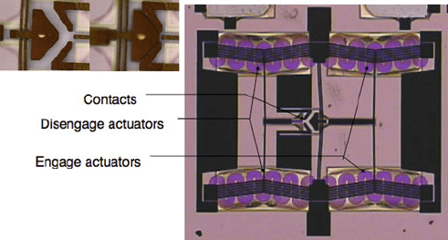
Figure 14.60 shows a photograph of an electrical relay actuator device made with
the MetalMUMPS
TM
process technology.
14.8.2.18 aMEMS
TM
(Teledyne)
The aMEMS
TM
process sequence was originally developed by Rockwell Scientific
(now Teledyne Scientific and Imaging, LLC) and is a versatile fabrication process
using silicon-on-insulator wafers. The process sequence involves the transfer of
14 MEMS Process Integration 1127
Fig. 14.60 Microactuator fabricated using the MetalMUMPS
TM
process technology (Reprinted
with permission, copyright MEMSCap, Inc.)
a silicon device layer to a receiving wafer using an adhesive layer. This process
sequence has been used to implement MEMS devices for a wide variety of applica-
tions, including RF tunable capacitors, switches, industrial process sensors, inertial
sensors, and many more [54–60].
Some of the key highlights of the aMEMS
TM
process include:
• Single-crystal silicon device layer for uniform material properties and low stress
levels for the structural layer.
• Silicon device layer is micromachined using DRIE enabling high-dimensional
control, repeatability, and uniformity.
• Multiple substrate materials can be used (e.g., silicon; high-resistivity silicon;
glass; etc.).
• All low-temperature processing (thermal budget is only 200
◦
C).
• Simple two-mask step process enabling rapid fabrication cycles and prototyping.
• High level of process flexibility to implement wide variety of device types.
The aMEMS
TM
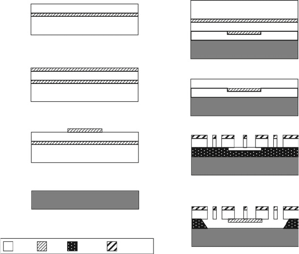
process sequence begins with a 100 mm SOI wafer with a han-
dle wafer thickness of 500 µm, a device layer nominally having a 20 µm thickness,
and a buried oxide layer having a thickness of 0.5 µm (Fig. 14.61a)[61]. A thin-
film layer of silicon dioxide having a nominal thickness of 1.6 µm is deposited
using plasma-enhanced chemical vapor deposition (PECVD) on the top surface of
the SOI silicon device layer at a temperature of 200
◦
C (Fig. 14.61b). This PECVD
silicon dioxide layer serves as a releasable insulator structural layer to thereby pro-
vide electrical isolation as well as mechanical connection between portions of the
to-be-defined single-crystal silicon device structural layer. Photolithography is per-
formed (Mask 1) on the top surface to pattern the silicon dioxide layer and the SiO
2
layer is etched using a reactive ion etch. Subsequently, the photoresist is removed
from the wafer (Fig. 14.61c).
A second substrate having a nominal thickness of 500 µm is selected accord-
ing to the intended application (Fig. 14.61d). For example, the second substrate
1128 M.A. Huff et al.
Silicon Wafer
(a). Starting wafer is a SOI wafer with a 20 micron
thick device layer, a 0.5 micron thick buried oxide
layer, and a 500 micron thick silicon handle wafer.
Silicon Wafer
(b). A 1.6 micron thick layer of Silicon Dioxide is deposited
on the top surface of the SOI wafer using PECVD.
Silicon Wafer
(c). Photolithography is performed (Mask Level 1) to
pattern the PECVD oxide which is then etched using
RIE.
(d). A second substrate is selected depending on the
application. Choices may include glass, high or low
resistivity silicon.
Second Substrate
Silicon Wafer
Second Substrate
(e). The SOI wafer and second substrate are bonded using
an adhesive layer nominally 20 microns in thickness.
Second Substrate
(f). The handle wafer and buried oxide layer of the SOI wafer are
removed.
Second Substrate
(g). A 0.5 micron thick layer of aluminum is evaporated and
photolithography is performed (Mask Level 2) to pattern and etch
aluminum layer. With photoresist left intact, the silicon layer is then
DRIE etched.
Second Substrate
Silicon
AluminumAdhesiveOxide
Fig. 14.61 Process sequence for the aMEMS
TM
process
can be either of low- or high-resistivity silicon, Pyrex 7740, or some other choice.
This second substrate is then bonded to the device layer of the SOI wafer using
an adhesive material (Fig. 14.61e). The adhesive is cured at 190
◦
C and has a
cured thickness of approximately 20 µm(±5 µm). The silicon handle wafer of
the SOI substrate is removed and subsequently the buried silicon dioxide layer is
also removed (Fig. 14.61f).
A layer of aluminum having a nominal thickness of 0.5 µm is deposited on the
silicon surface of the composite substrate using evaporation (Fig. 14.61g). This alu-
minum layer can be used to provide electrical contact to the silicon device layer.
A second photolithographic step is performed on the top surface of the substrate
followed by a RIE of the aluminum layer. Without removing the photoresist used to
mask the aluminum layer, the substrate is etched using DRIE to transfer the pattern
into the silicon device layer. The photoresist is then completely r emoved.
The substrate is then exposed to an oxygen plasma that selectively etches the
exposed adhesive layer to release the silicon device. Given the isotropic nature of the
oxygen plasma release, there is some undercutting of the silicon at the boundaries
of the device (Fig. 14.61h). Lastly, the wafer can be diced and packaged.
Alternatively, the silicon device layer may be released subsequent to dicing.
Although this approach requires the fabricator to handle and release individual die,
there is some advantage in dicing the substrate before the release of the silicon
devices.
14 MEMS Process Integration 1129
The aMEMS
TM
process sequence is applicable to implementing a diversity of
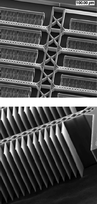
different MEMS device types. Figure 14.62 is a SEM image of a tunable capaci-
tor implemented using the aMEMS
TM
process sequence. Tuning is achieved using
electrostatic actuation by applying a voltage potential to interdigitated electrodes
that are nominally 20 µm in height and have a gap spacing of 2 µm. When a volt-
age potential is applied to the device, the electrostatic forces move the structure
thereby changing the capacitance (by changing the capacitor electrode gap spac-
ing). The silicon capacitor structure is supported by silicon flexures and the stiffness
of these flexures can be adjusted over a range according to the design require-
ments. Figure 14.63 is a SEM of very high-aspect-ratio structures made with the
aMEMS
TM
process sequence.
Fig. 14.62 SEM image of
tunable capacitor fabricated
using the aMEMS
TM
process
module (Reprinted with
permission, copyright
Teledyne Scientific and
Imaging Company)
Fig. 14.63 Close-in view
SEM image of tunable
capacitor fabricated using the
aMEMS
TM
process module.
Thefingersare80µmin
height and only 2 µmin
width (Reprinted with
permission, copyright
Teledyne Scientific and
Imaging Company)
1130 M.A. Huff et al.
14.8.2.19 Plastic MEMS (University of Michigan)
The plastic/polymer MEMS (PMEMS) process was developed at the University
of Michigan [62] and has found application in implementing sensors (including
chemical, gas, and biological sensors), capillary electrophoresis devices (including
DNA analysis, gene research), and integrated microfluidic networks and systems
(including drug analysis, drug synthesis, disease detection, and pharmaceutical
research and development).
The PMEMS process utilizes surface micromachining techniques of polymer-
based structural and sacrificial layers to implement a diversity of MEMS devices
for applications for the microfluidics and bio/nano microsystems. Although the
PMEMS process has mostly used Parylene-C as the polymer in fabrication, other
polymers can be used depending on the intended application. Among the advantages
of using Parylene in the PMEMS process include: parylene film used as a structural
layer is highly conformal, pinhole free, and deposited at low temperatures; Parylene
has a low outgasing and low permeability to both gases and fluids as compared to
other polymers; Parylene is chemically inert; and is considered to be biocompatible.
Furthermore, given these properties, specifically the low process temperatures, the
PMEMS Parylene process can be relatively easily integrated with microelectron-
ics. The disadvantages of the Parylene PMEMS process are that even though the
Parylene has lower permeability than other polymers, it still has a finite permeability.
Consequently, if Parylene is left in a strong acid, base, or solvent for any extended
period of time, the solution will permeate through the Parylene film and attach to
the adhesion layer, thereby resulting in the Parylene peeling from the substrate sur-
face. In addition, devices and systems implemented using the Parylene PMEMS
process are restricted to applications of less than 90
◦
C. Temperatures higher than
90
◦
C coupled with the high thermal expansion coefficient of Parylene will result in
large thermal stress between the film and the substrate and the film will delaminate
from the substrate.
The process is relatively simple, having only three masking steps in the basic
process (five masking steps for the more advanced PMEMS process variation),
and therefore can be used for very fast production cycle times as well as rapid
prototyping. The PMEMS process can be performed on a variety of different
substrate types including polycarbonate, silicon, glass, and others. The nominal pro-
cess allows for channel heights typically ranging from 1 to 50 µm, channel widths
up to 200 µm, and channel lengths up to 1.5 cm for sealed channels and 2.7 cm for
channels with access holes. The PMEMS process is sufficiently simple and flexi-
ble that it can be relatively easily combined with additional processing steps and/or
modules to implement other components such as microvalves and micropumps.
The generic PMEMS process utilizing Parylene-C as the channel material and
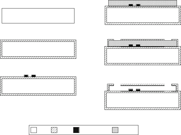
the fabrication being performed on a glass substrate is described (See Figs. 14.64
and 14.65). A glass substrate, having a thickness of approximately 1 mm, is first
cleaned using an appropriate cleaning solution such as a piranha etch to remove
all organic materials and particulates from the surface (Fig. 14.64a). Subsequently,
the substrate is then coated with a 6 µm thick layer of Parylene on both sides to
14 MEMS Process Integration 1131
Glass Substrate
Glass Substrate
(a). Starting substrate is polycarbonate or glass
although other substrate types can be easily used.
(b). The substrate is coated on both sides with a
layer of Parylene that is 6 um in thickness.
Glass Substrate
(c). A layer of Chrome (30 nm in thickness) and Gold (500
nm in thickness) is deposited and patterned to form
electrodes (Mask Level 1).
Glass Substrate
(d). A 10 um thick layer of photoresist is deposited and
patterned (Mask Level 2).
Glass Substrate
(e). A 3 um thick layer of parylene is deposited using CVD
and subsequently patterned (Mask Level 3).
(f). The sacrificial photoresist layer is removed using acetone
immersion.
Glass Substrate
Silicon Parylene PhotoresistChrome/Gold Layer
Fig. 14.64 Basic PMEMS process sequence
prevent substrate damage during fabrication (Fig. 14.64b). A layer of chrome hav-
ing a thickness of 30 nm, followed by a layer of gold having a thickness of 500 nm is
deposited on the top surface of the substrate using evaporation. This metal layer typ-
ically is used to make electrodes and microheaters in the devices. Photolithography
is then performed (mask level 1) on the chrome and gold metal layers on the top
surface to define these metal layers into the desired pattern (mask level 1) as shown
in Fig. 14.64c.
A layer of photoresist having a thickness of 10 µm is then deposited on the
top surface of the substrate using spin deposition (Fig. 14.64d). This layer acts as
the sacrificial layer for making the channels and its thickness can be adjusted so
as to vary the channel height. Photolithography is then performed to pattern the
photoresist layer (mask level 2). A 3 µm thick Parylene layer is deposited onto the
substrate at room temperature using chemical vapor deposition (CVD). Parylene
deposition is extremely conformal over the topology of the sacrificial photoresist
layer and is used to form the channel walls. Subsequently, a 10 µm thick layer
of photoresist is spun deposited and patterned (mask level 3) to make openings in
the top Parylene film layer. These openings are used to release the channels by
removing the photoresist sacrificial layer. These release openings have a maximum
spacing of 1.5 mm according to the release time of the standard process. After the
masking photoresist is defined, the Parylene is etched using an oxygen plasma etch
(Fig. 14.64e). The substrate is then immersed in acetone for approximately 8 h,
followed by two additional acetone and isopropanol alcohol rinses to completely
remove the photoresist sacrificial material from inside the channels (Fig. 14.64f).
1132 M.A. Huff et al.
(a). Deposition of a 6 um thick layer of parylene using CVD.
(e). Connection of external fluidic lines.
Glass Substrate
(b). Deposition and patterning of a Titanium masking layer
(Mask Level 4).
Glass Substrate
(c). Deposition and patterning of 75 um thick layer of SU-8.
Glass Substrate
(d). Etching of exposed parylene in oxygen plasma to open
fluidic ports and electrical contact pads.
Glass Substrate
Glass Substrate
Silicon Parylene PhotoresistChrome/Gold Layer Titanium SU-8 External Lines
Fig. 14.65 Additional process steps for PMEMS process in order to make fluidic connections
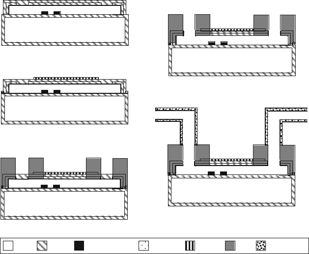
For many applications it is desirable to apply pressure to the fluids inside the
channels and the ability to do this requires additional processing to seal the release
openings. Therefore, for this purpose a 6 µm thick layer of Parylene is deposited at
room temperature using CVD (Fig. 14.65a). Next, a 0.5 µm thick layer of titanium
is deposited using evaporation onto the top surface of the substrate and patterned
using photolithography and wet etching (mask level 4; Fig. 14.65b). The titanium
layer masks most of the substrate surface and is only exposed in the areas designated
for fluid interconnects and electrical contacts. Subsequently, a 75 µm thick layer
of SU-8 is spun deposited onto the top substrate surface. Photolithography is then
performed on the SU-8 layer (mask level 5) to pattern the SU-8 layer (Fig. 14.65c).
The substrate is then placed into a reactive ion etcher and using an oxygen plasma,
the Parylene material exposed under the SU-8 and titanium layers is removed by
etching (Fig. 14.65d). The titanium layer exposed on the substrate surface is then
removed using a wet chemical immersion. Lastly, external fluidic connections are
made to the SU-8 layer by pressing appropriate-sized fluidic tubing to the SU-8
device connections (Fig. 14.65e).
14.8.2.20 Wafer-Level Packaging (ISSYS)
The wafer-level packaging module developed by Integrated Sensing Systems
(ISSYS) is one approach used to simplify, standardize, and lower the cost of
14 MEMS Process Integration 1133
MEMS packaging (Fig. 14.66)[63]. The basic idea is to use MEMS processing
technologies, including micromachining and wafer bonding, to build an effective
ambient-controlled encapsulation around the MEMS device using batch-fabrication
techniques. The features of the wafer-level packaging include: it simplifies the rest
of the assembly and packaging, improves yield throughout the remainder of the
production process, allows utilization of standard assembly, packaging and test
equipment, and allows a sustainable vacuum-sealing of the MEMS to levels below
1 mtorr. This last feature is particularly important for MEMS devices such as iner-
tial and resonator devices, which require high-vacuum levels that are able to be
maintained for long periods of time [64].
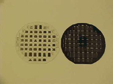
Fig. 14.66 MEMS device
wafer (left) prior to bonding
and capping wafer (right)
(Courtesy of ISSYS Inc.)
The high-vacuum, wafer-level packaging technology is defined as a process mod-
ule due to the fact that this sequence of processing steps is really only useful
when combined with the fabrication of MEMS devices [65]. The process module
can be used with a variety of MEMS process technologies including: surface
micromachining, bulk micromachining, silicon-on-glass, LIGA, and others. The
process module begins with either the choice of a silicon or Pyrex 7740 capping
wafer having the same diameter as the s ubstrate in which the MEMS devices are
fabricated. This capping wafer will be used to bond and encapsulate the MEMS
device wafer.
Micromachining is performed on the silicon or glass capping wafer to create a
recess or cavity in the substrate (Fig. 14.67). The technique used to make the recess
varies depending on the type of substrate material as well as the depth of the recess
to be made, but as an example, DRIE anisotropic etching would be an appropriate
method for creating the recess in a silicon capping wafer (Fig. 14.67b). Through-
wafer vias are then etched through the silicon or glass capping wafer, which will
allow electrical connection to the MEMS devices once they are encapsulated in the
wafer-level package (Fig. 14.67b). Next, a sealing material, such as glass frit or
solder, is deposited and patterned on the capping wafer (Fig. 14.67c). A proprietary
NanoGetter
TM
material is then applied and patterned such that it is located in the
recesses made in the capping wafer (Fig. 14.67d). The capping wafer is then bonded
to the MEMS device wafer using a vacuum ambient during the bonding procedure
