Ghodssi R., Lin P., MEMS Materials and Processes Handbook
Подождите немного. Документ загружается.


1074 M.A. Huff et al.
Acceptance
Range
Near 0%
Yield
Acceptance
Range
Near 100%
Yield
(a) (b)
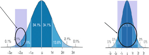
Fig. 14.12 The importance of precision and control of manufacturing processes on the yield.
(a) Widely spread Gaussian curve for a manufacturing process that has significant variations and
a bias offset error thereby resulting in a low yield given by the overlap of the acceptance range
and the Gaussian curve. (b) Manufacturing process that has considerably less variation and no
bias offset error and therefore has a high yield (Reprinted with permission, copyright MEMS and
Nanotechnology Exchange)
The important point of this discussion is that the designs of the device and the
process sequence have an enormous impact on how easy it is to produce a device
that meets its required performance specifications. Although very difficult to do in
practice, it is extremely important to ensure that the process sequence, materials,
equipment, and design all strive to the extent possible to reduce the variations in the
fabrication process and the resultant device behavior.
14.7.5 Package Design and Assembly
Design for manufacturing in the area of package-device interactions can also be
quite complex. The main area where package and assembly variations can translate
into performance variations is stress. In the process of assembly, a MEMS die will
be bonded to a substrate, wire bonded, and then either lid sealed or overmolded. All
of these processes occur at elevated temperatures and impart stresses on the MEMS
die. The chance that such a complex system would revert to a stress-free state at the
device’s operating temperature is very unlikely. Manufacturing variations are also
caused by variations in the placement of the die in the package, which can change the
stress state. It can also directly affect the device’s cross-axis performance by causing
variations in the package-to-device coordinate reference frames. Finally, the intra-
package interconnect (e.g., wirebonds) can cause variation in parasitic capacitances
that can affect device performance.
Clearly the variations caused by packaging and assembly are very complex.
Designing to reduce these variations is similarly complex. Good design for man-
ufacturability requires an understanding of these physical interactions. The most
effective method for analyzing the variations and optimizing a design is through the
use of 3-D simulation. This still requires an understanding of the underlying mate-
rial properties as an input, but it allows the designer to examine material variations,
14 MEMS Process Integration 1075
design geometry variations, and environmental use cases (i.e., temperature and
humidity).
14.7.6 System Design for Manufacturability
Some of the major issues related to design for manufacturability of the system, such
as whether to integrate the MEMS with microelectronics on the same substrate were
discussed above. This may be the most important decision in any MEMS develop-
ment effort, however, it is not the only design for manufacturability systems-related
issue. Another systems-related issue is how to calibrate the device. Due to the large
variations in the critical dimensions of MEMS sensors it is not uncommon that some
postfabrication calibration must be performed. Often this is done by laser-cutting
an array of “trim resistors” that are part of the sensor output signal circuitry. The
design of the MEMS device and associated microelectronics must consider how
any required calibration is to be performed. Moreover, at what stage the calibration
and final testing are performed is also important. Although the yield at the com-
pletion of the frontend fabrication may be relatively high, the yield can be reduced
dramatically in complex assembly and packaging processes and therefore it may be
less expensive to trim the devices after they are assembled, packaged, and tested to
be functional.
Some MEMS devices, such as liquid drop ejectors and micromirror diffraction
gratings, contain an array of actuators that need to operate relatively equally in order
to meet their performance requirements. Compared to the effort to fabricate every
actuator with little variation, it is sometimes easier to take care of the variation at the
system level. For example, the individual actuators can be calibrated and the input
power for each actuator can be adjusted according to the calibration to have equal
output. This is to consider the design for manufacturability from a system point of
view.
14.7.7 Environmental Variations
Once the MEMS device is installed in the field, it will be subjected to a range
of environmental conditions. The most widely encountered are variations in tem-
perature and humidity. As we saw in the discussion of packaging variations, the
complicated in-package stress state of a MEMS device is temperature-dependent,
due to the differences in the coefficients of thermal expansion of all the materials
in the device and its package. Variations in humidity can have a similar effect on
the packaged device’s stress state. Humidity variations have much more complex
material interactions and time constants than temperature interactions, so modeling
them can be much more difficult. There are many other environmental variations
that can affect device performance, such as: electromagnetic interference (EMI),
static charge, vibration, and so on. Design to reduce the effects of these variables is
complex and requires a great deal of experience with the specific use environment
of a given MEMS device.
1076 M.A. Huff et al.
14.7.8 Test Variations
Many MEMS devices are sensors whose scale factor is calibrated during a final
test procedure. Variations in this test procedure can lead to variations in perfor-
mance due to scale factor inaccuracy. Again, variations of this type can be very
complex to model or understand. Most often this type of variation is reduced by
having test guard-bands, which ensure that the device remains “in-spec” in spite of
tester variation.
14.7.9 Recommendations Regarding Design for Manufacturability
Clearly, design for manufacturability in MEMS development and production is
extremely complex and challenging. Nevertheless, there are some basic tenets that
are generally applicable and useful to follow. The list below is a set of recommen-
dations that a MEMS developer can employ in the pursuit of achieving design for
manufacturability in her MEMS development efforts.
1. Keep the design and process sequence as simple as possible: More process-
ing steps and a more complicated design will make for lower yields, longer
development times, and higher costs.
2. Leverage from existing process modules and technologies to the extent possi-
ble: This will lower your development (nonrecurring engineering or NRE) cost
and time as well as reduce risk.
3. Know the physics of your device and how they relate to the dimensions and
fabrication process. Avoid fabrication processes that provide large relative
tolerances of the dimensions for critical elements, particularly those having
higher-order dependencies (i.e., to the square, cube, or fourth power). Use bi-
stable mechanical elements to the extent possible; the large relative tolerances
of MEMS devices make continuous-movement device types hard to implement
and costly to calibrate.
4. Make critical mechanical elements from materials having reproducible proper-
ties: Making devices from materials such as single-crystal silicon can be far
easier than making them from thin-film materials. Avoid designs that criti-
cally depend on the hard-to-control fabrication processes such as perpendicular
etched sidewalls, timed etching depth, and sidewall smoothness.
5. Use processing recipes and tools that are well proven to the extent possi-
ble: Avoid new equipment and new process capabilities until they are well
proven and shown to be reliable and able to deliver reproducible results. Use
appropriate etch stop layers and endpoint detection to accommodate etch rate
variations.
6. Minimize the number of materials and layers that comprise the critical mechan-
ical elements: Stacking of multiple material layers of thin films is only asking
for big challenges.
7. Understand and account for the respective relative tolerances in the precision
of the fabrication methods employed.
14 MEMS Process Integration 1077
8. Expect to make several design and process changes as well as multiple itera-
tions in the development of a viable process sequence: Patience for multiple
iterations is the name of the game in MEMS development.
9. Avoid merging MEMS with microelectronics on the same substrate unless the
application demands it: Integrated MEMS is a costly and risky strategy.
10. Engage packaging, assembly, and test engineers into the device development
effort at the beginning of the design process: All these parties must work closely
together, listen, and be ready to compromise to achieve a successful outcome.
The fabrication–validation cycle takes a long time. Perform as much multi-
physics simulation as possible to optimize design critical parameters and reduce
the development cycle time.
11. Embed smart test structures in the layout to determine material properties and
performance: This is critical and useful when diagnosing the failure mode and
understanding the fabrication problems.
14.8 Review of Existing Process Technologies for MEMS
It is very instructive to review some of the existing fabrication methods that have
been successfully developed with an eye toward why they are structured in the way
that they are. Therefore, we review a number of successful examples of MEMS
process sequences and explain some of the issues and tradeoffs that were con-
fronted during development. We begin reviewing nonintegrated MEMS process
sequences and then move to examining several examples of integrated MEMS pro-
cess sequences. To the extent possible, we have attempted to select examples of
process sequences that have been developed for the commercial market and which
represent as broad a sampling of implementation practices as possible.
14.8.1 Process Selection Guide
Table 14.1 is a listing of all of the nonintegrated and integrated MEMS process
sequences that we review in this chapter. The name of the process sequence and
the entity that developed it are provided followed by several high-level differentia-
tors such as device application, whether it is integrated with microelectronics, the
type of micromachining processes used, the functional material used in the device,
the aspect ratio of the process, whether the process sequence is suitable for imple-
menting moving or static elements, whether one or both sides of the substrate are
processed, and whether the process sequence (or a derivative) has been used in
commercial production.
14.8.2 Nonintegrated MEMS Process Sequences
14.8.2.1 PolyMUMPS
TM
(MEMSCAP)
Please note the nomenclature used below: ALLCAPS refers to the mask-level name;
lower caps refers to the deposition layer name.

1078 M.A. Huff et al.
Table 14.1 Process sequences reviewed in this chapter
Process sequence
name Designer/developer
Device
application
Nonintegrated
or integrated
Technology
employed
Functional
material Aspect ratio
Comm.
production
PolyMUMPS
TM
MEMSCap Variable Non Surface Polysilicon Low Yes
FBAR Avago RF filters Non Bulk and
surface
AlN Low Yes
SUMMiT V Sandia Variable Non Surface Polysilicon Low Yes
a
Microphone Knowles Acoustic
sensor
Non Bulk and
surface
Polysilicon Low Yes
Resonator SiTime Timing
oscillator
Non Surface Single-crystal
silicon
Medium Yes
Gyroscope Draper Inertial
sensing
Non Surface Single-crystal
silicon
Low Yes
b
THELMA STMicroelectronics Inertial
sensing
Non Bulk Polysilicon Medium Yes
Pressure Sensor Novasensor Pressure
sensing
Non Bulk Single-crystal
silicon
Low Yes
Bulk Accelerometer Ford Microelectronics Inertial
sensing
Non Bulk Silicon Low Yes
c
SCREAM Cornell University Variable Non Bulk Polysilicon High Yes
d
HARPSS University of Michigan Variable Non Bulk SCS and
polysilicon
High Yes
e
Hybrid MEMS Infotonics MOEMS Non Bulk and
surface
Single-crystal
silicon
Medium No
Silicon-On-Glass
(SOG)
University of Michigan Variable Non Bulk Single-crystal
silicon
Medium No
SOIMUMPS
TM
MEMSCap Variable Non Bulk and
surface
Single-crystal
silicon
High Yes
LIGA CAMD Variable Non Bulk Nickel High No
RF MEMS Switch MEMtronics RF Switches Non Surface Aluminum Low Yes

14 MEMS Process Integration 1079
Table 14.1 (continued)
Process sequence
name Designer/developer
Device
application
Nonintegrated
or integrated
Technology
employed
Functional
material Aspect ratio
Comm.
production
MetalMUMPS
TM
MEMSCap Variable Non Bulk and
surface
Nickel Medium Yes
aMEMS
TM
Teledyne Variable Non Bulk Single-crystal
silicon
High No
Plastic MEMS University of Michigan Microfluidics Non Surface Paralene Low No
Wafer-Level
Packaging
ISSYS Packaging Non Bulk Silicon or glass N/A Yes
iMEMS Analog Devices Inertial
Sensing
Integ. Surface Polysilicon Low Yes
DLP Texas Instruments Displays Integ. Surface Aluminum Low Yes
Integrated Pressure
Sensor
Freescale Pressure
Sensing
Integ. Bulk Single-crystal
silicon
Low Yes
Thermal Inkjet Xerox Printing Integ. Bulk and
Surface
Single-crystal
silicon
Medium Yes
Microbolometer Honeywell Infrared
sensing
Integ. Surface Vanadium oxide Low Yes
ASIM-X CMU Variable Integ. Bulk SCS and/or
CMOS layers
Low Yes
f
CMOS+MEMS Wispry RF Integ. Surface Copper and gold Low Yes
Integrated SiGe
MEMS
University of California
at Berkeley
Variable Integ. Surface Silicon
germanium
Low No
Integrated SUMMiT Sandia Variable Integ. Surface Polysilicon Low No
a
Licensed to Fairchild Semiconductor, but production has been discontinued
b
A derivative of this process has been licensed for commercial production
c
Developed for production and then discontinued
d
A derivative of this process technology is in production at Kionix
e
Licensed to Qualtre Inc. for commercial production
f
Licensed to Akustica and a derivative of process technology is in production
1080 M.A. Huff et al.
The PolyMUMPS
TM
process is part of the MUMPs
R
(Multiuser MEMS pro-
cesses) prototyping program that was originally developed by the Microelectronics
Center of North Carolina (MCNC) under contract from the Defense Advanced
Research Projects Agency (DARPA) and is now offered by MEMSCAP Inc. out
of the same facility in Research Triangle Park, NC. The objective was to develop a
standardized process that could be made available on a periodic basis to the research
community in a multiuser environment. The PolyMUMPS process is a three-layer
polysilicon surface micromachining process derived from work performed at the
University of California at Berkeley in the late 1980s and early 1990s. This process
is the most widely known and used process for implementing MEMS in the world
and has been offered continuously since 1992. Over 80 PolyMUMPS process runs
have been completed to date for hundreds of organizations around the world.
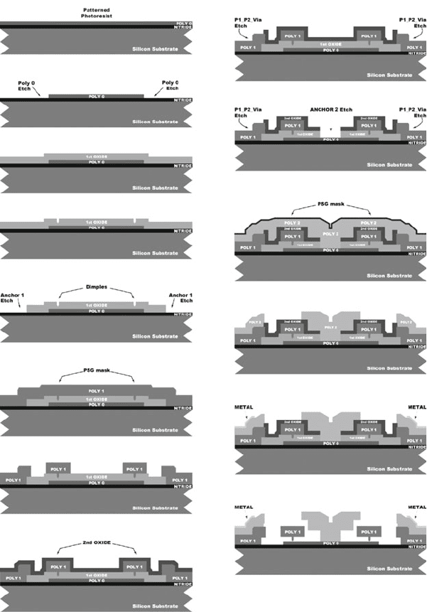
The process begins with 150 mm n-type (100) silicon wafers of 1–2 cm resis-
tivity (Fig. 14.13)[3]. The surfaces of the wafers are first heavily doped with
phosphorus in a standard diffusion furnace using a phosphosilicate glass (PSG)
sacrificial layer as the dopant source. This helps to reduce or prevent charge
feedthrough to the substrate from electrostatic devices on the surface. Next, after
removal of the PSG film, a 600 nm low-stress LPCVD (low pressure chemical
vapor deposition) silicon nitride layer is deposited on the wafers as an electrical
isolation layer. This is followed directly by the deposition of a 500 nm LPCVD
polysilicon film, Poly 0. Poly 0 is then patterned by photolithography, a process that
includes the coating of the wafers with photoresist, exposure of the photoresist with
the appropriate mask, and developing the exposed photoresist to create the desired
etch mask for subsequent pattern transfer into the underlying layer (Fig. 14.13a).
After patterning the photoresist, the Poly 0 layer is then etched in a plasma etch
system (Fig. 14.13b). A 2.0 µm phosphosilicate glass (PSG) sacrificial layer is then
deposited by LPCVD (Fig. 14.13c) and annealed at 1050
◦
C for 1 h in argon. This
layer of PSG, known as First Oxide, is removed at the end of the process to free
the first mechanical layer of polysilicon. The sacrificial layer is lithographically pat-
terned with the DIMPLES mask and the dimples are transferred into the sacrificial
PSG layer in an RIE (Reactive Ion Etch) system, as shown in Fig. 14.13d. The nom-
inal depth of the dimples is 750 nm. The wafers are then patterned with the third
mask layer, ANCHOR1, and reactive ion etched (Fig. 14.13e). This step provides
anchor holes that will be filled by the Poly 1 layer.
After etching ANCHOR1, the first structural layer of polysilicon (Poly 1) is
deposited at a thickness of 2.0 µm. A thin (200 nm) layer of PSG is deposited
over the polysilicon and the wafer is annealed at 1050
◦
C for 1 h (Fig. 14.13f). The
anneal dopes the polysilicon with phosphorus from the PSG layers both above and
below it. The anneal also serves to significantly reduce the net stress in the Poly
1 layer. The polysilicon (and its PSG masking layer) is lithographically patterned
using a mask designed to form the first structural layer POLY1. The PSG layer
is etched to produce a hard mask for the subsequent polysilicon etch. The hard
mask is more resistant to the polysilicon etch chemistry than the photoresist and
ensures better transfer of the pattern into the polysilicon. After etching the polysili-
con (Fig. 14.13g), the photoresist is stripped and the remaining oxide hard mask is
removed by RIE.

14 MEMS Process Integration 1081
(a). Patterned Photoresist
(b). Poly0 Etch
(c). 1
st
Oxide Deposition
(d). 1
st
Oxide Dimple Etch
(e). 1
st
Oxide Anchor1 Etch
(f). Poly1 and Hard Mask Deposition
(g). Poly1 Etch
(h). 2
nd
Oxide Deposition
(i). POly1/POly2 Via Etch
(j). Anchor 2 Etch
(k). Poly2 and Hard Mask Deposition
(l). Poly2 Etch
(m). Metal Deposition
(n). Released Structure
Fig. 14.13 Cross-section of wafer during processing steps of the MEMSCap PolyMUMPS process
sequence (Reprinted with permission, copyright MEMSCap, Inc.)
After Poly 1 is etched, a second sacrificial PSG layer (Second Oxide, 750 nm
thick) is deposited and annealed (Fig. 14.13h). The Second Oxide is patterned using
two different etch masks with different objectives. The POLY1_POLY2_VIA level
provides for etch holes in the Second Oxide down to the Poly 1 layer. This provides
a mechanical and electrical connection between the Poly 1 and Poly 2 layers.

1082 M.A. Huff et al.
The POLY1_POLY2_VIA layer is lithographically patterned and etched by RIE
(Fig. 14.13i). The ANCHOR2 level is provided to etch both the First and Second
Oxide layers in one step, thereby eliminating any misalignment between separately
etched holes. More important, the ANCHOR2 etch eliminates the need to make a cut
in First Oxide unrelated to anchoring a Poly 1 structure, which needlessly exposes
the substrate to subsequent processing that can damage either Poly 0 or Nitride. The
ANCHOR2 layer is lithographically patterned and etched by RIE in the same way
as POLY1_POLY2_VIA.
Figure 14.13j shows the wafer cross-section after both POLY1_POLY2_VIA and
ANCHOR2 levels have been completed. The second structural layer, Poly 2, is then
deposited (1.5 µm thick) followed by the deposition of 200 nm of PSG. As with
Poly 1, the thin PSG layer acts as both an etch mask and dopant source for Poly 2
(Fig. 14.13k). The wafer is annealed to dope the polysilicon and reduce the resid-
ual film stress. The Poly 2 layer is lithographically patterned with the seventh mask
(POLY2). The PSG and polysilicon layers are etched by plasma and RIE processes,
similar to those used for Poly 1. The photoresist is then stripped and the masking
oxide is removed (Fig. 14.13l).The final deposited layer in the PolyMUMPs pro-
cess is a 0.5 µm metal (Au with Cr adhesion layer) layer that provides for probing,
bonding, electrical routing, and highly reflective mirror surfaces. The wafer is pat-
terned lithographically with the eighth mask (METAL) and the metal is deposited
and patterned using liftoff. The final unreleased structure is shown in Fig. 14.13m;
Figure 14.13n shows the device after sacrificial oxide release using HF.
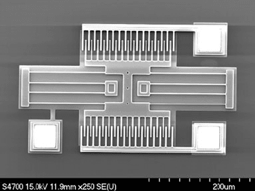
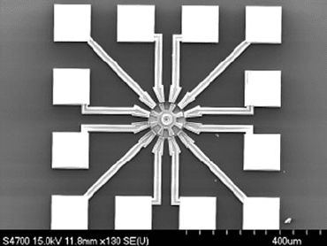
Figures 14.14 and 14.15 are SEMs of MEMS devices made using the MUMPS
process sequence. Figure 14.14 is a SEM of a comb-drive resonator and Fig. 14.15
is a SEM of an electrostatically actuated micromotor.
Fig. 14.14 SEM of a
comb-drive resonator
microstructure made using
MEMSCap’s MUMPS
process sequence (Reprinted
with permission, copyright
MEMS and Nanotechnology
Exchange)
14.8.2.2 Film Bulk Acoustic-Wave Resonators (FBARs) (Avago)
Piezoelectric materials (see Chapter 5) are used to convert electrical energy into
mechanical energy and vice versa. Thin-film bulk acoustic resonators (FBARs)
are two-terminal devices that utilize a thin-film layer of a piezoelectric mate-
rial sandwiched between two metal electrodes. In the limit of infinitesimally thin

14 MEMS Process Integration 1083
Fig. 14.15 SEM of an
electrostatically actuated
micromotor made using
MEMSCap’s MUMPS
process sequence (Reprinted
with permission, copyright
MEMS and Nanotechnology
Exchange)
electrodes, a resonance condition is met when the thickness of the piezoelectric
material is equal to an integer multiple of half of the acoustical wavelength of the
piezoelectric material at the desired electrical driving frequency. More specifically,
the fundamental resonant frequency is proportional to the ratio of the acoustic veloc-
ity in the piezoelectric material and twice the thickness of the resonator. With finite
electrodes the resonant frequency shifts downward with the additional mass loading.
Although there are different configurations of acoustic-wave devices, the FBARs
use an electrical driving field through the thickness of the resonator to generate a
longitudinal or compression acoustical wave along the same direction. The thick-
nesses of the thin-film piezoelectrics can be quite small, thereby allowing FBARs
devices to resonate at high frequencies. The FBAR configuration with an air inter-
face on either side combined with the ability to fabricate devices using materials
having high-Q’s (i.e., quality factors) provides for a resonator having very high
intrinsic Q, a prerequisite for good filter performance. In addition, the air interface
of FBARs also allows the effective coupling coefficient to be maximized compared
to other configurations. Lastly, FBARs can handle relatively high powers and pos-
sess good thermal stability [4]. As a result of these advantages, FBAR technology
has rapidly grown into a very large commercial market with the primary application
area being electronic filters for cellular telephones [5]. The distinct advantages of
FBARs over competitive technologies are its physical properties, specifically: a high
resistance to electrostatic discharge (ESD); good temperature stability; and excel-
lent insertion loss in the passband (due to high Q) combined with excellent rejection
and isolation out-of-band. All of these features are provided in a very small-sized
package footprint for use by handset manufacturers [6].
FBARs are an interesting process integration example because they employ a
piezoelectric material, which is an exotic material type that requires special material
and processing compatibility considerations. Moreover, the need to appropriately
manage the inherently large acoustic impedance mismatch resulting from having
the resonator structure located on the surface of the substrate presents several major
design and fabrication challenges as well. This mismatch results from having one
side of the resonator exposed to air and the other affixed onto the wafer surface.
