Zuo-Guang. Ye Advanced Dielectric Piezoelectric and Ferroelectric Materials: Synthesis, Characterisation and Applications
Подождите немного. Документ загружается.

Handbook of dielectric, piezoelectric and ferroelectric materials1020
These reactions proceed quickly and do not limit the vacancy formation
reaction. In contrast, O
ad
has to meet another O
ad
on the surface to form an
O
2
molecule, which then diffuses into the atmosphere. The reaction related
to O
ad
that is suppressed at a higher
P
O
2
is the limiting factor of the vacancy
formation for BiT. Therefore, only model 3 can account for the
P
O
2
dependence
of weight loss. The formation of
′′′
V
Bi1
brings about
V
O1
••
for charge
compensation in the crystal as expressed by eq. (33.1). High-
P
O
2
atmosphere
inhibits the reaction on the crystal surface, and thereby further creation of
V
O1
••
is restricted, which prevents
′′′
V
Bi1
generation. Thus, a high
P
O
2
during
heating is effective for suppressing the vacancy formation in the lattice, i.e.
synthesizing high-quality BiT crystalline samples [19].
33.5 Domain structure
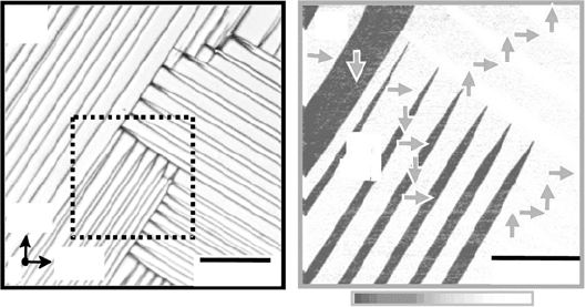
Figure 33.12 shows the domain structure in the a–b plane of a BiT crystal.
In the optical micrograph (Fig. 33.12a), taken in the transmission mode, a
striped 90° domain structure is clearly seen, similar to that reported for
BaTiO
3
single crystals [45] and PZT ceramics. Furthermore, a needle-like
domain structure is also observed, and the needlepoints are terminated at
domain walls. This kind of complex domain structure has been reported for
PbTiO
3
thin films [46] and predicted by Li et al. [47]. The striped domain
structures are observed at temperatures below the Curie temperature
(T
C
= 675°C) and disappear above T
C
.
Figure 33.12(b) shows the piezoresponse-force microscope (PFM) image
for the area indicated by the dashed square in Fig. 33.12(a). White (the
strongest PFM signal) and black (the weakest one) areas have the domains
with P
s
oriented in upper and lower direction, respectively, while the gray
(a)
(b)
100µm
b
(
a
)
a
(
b
)
c
P
s
50µm
170 mV–160mV
33.12
(a) Domain structure of a BiT crystal in the
a
–
b
plane observed
with optical microscopy, and (b) piezoelectric-force microscopic
image of the area denoted by the dashed line in (a).
WPNL2204
Crystal structure and defect control 1021
color indicates the domain with P
s
oriented in the horizontal direction. The
dark lines observed in the optical micrograph are 90° domain walls. In
addition to the striped 90° domains, 180° domain walls with head-to-head
and tail-to-tail configurations are seen in some of needle-like 90° domains.
These ‘charged’ domain walls are known to strongly interact with
V
O
••
[11, 19].
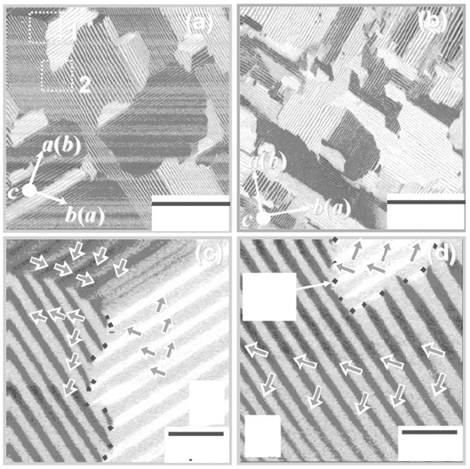
Figure 33.13 shows the PFM images of Bi
4–x
La
x
Ti
3
O
12
(BLT, x = 0.85 and
1.2) crystals. La substitution led to a significant change in domain structure,
and the domain size decreases with an increase in La content (x). In contrast
to BiT, gentle and irregular curvatures were found, and striped 90° domain
structures are constructed in the area framed by the curvatures. The enlarged
micrographs of the dashed square denoted by ‘1’ and ‘2’ in Fig. 33.13(a) are
indicated in Fig. 33.13(c) and (d), respectively. Surprisingly, all the striped
90° domains are regularly terminated at the curvature, implying that not only
do domains interact with the neighbors but also that a widespread interaction
plays a crucial role in the formation of the domain structure in the BLT
crystals.
5 µm5µm
P
s
180°
domain
wall
50 µm50 µm
P
s
33.13
Piezoelectric-force microscopic images of BLT crystals: (a) BLT
(
x
= 0.85) and (b) BLT (
x
= 1.20). The enlarged micrographs of the
dashed square denoted by ‘1’ and ‘2’ in (a) are indicated in (c) and
(d), respectively.
WPNL2204
Handbook of dielectric, piezoelectric and ferroelectric materials1022
The curvature observed in the middle of Fig. 33.13(c) is composed of two
different parts. One is the wall between the domains with upper- and lower-
oriented P
s
, showing a tail-to-tail 180° domain wall. The other between these
180° domain walls is the part with no change in PFM signal, indicating that
the direction of P
s
does no change regardless of the curvature. If striped 90°
domains have a standard structural configuration with an alternative 90°
rotation of the a and b-axes, the domains with the same PFM signal separated
by the curvature should have the opposite b-axis distortion (the opposite
TiO
6
distortion along the b-axis, as discussed below). These domains can be
superimposed on each other after a translation operation of [1/2 1/2 0],
suggesting that the other part of the curvature is an antiphase domain boundary
(ADB), as observed in the ceramics of BLT [30] and SrBi
2
Ta
2
O
9
[48].
Furthermore, on the upper left in Fig. 33.13(c), a head-to-head 180° domain
wall as well as ADB is also observed.
Here, domain structures are discussed in terms of ferroelectric and
ferroelastic distortions. 90° domains are formed to relieve mechanical stress
induced by ferroelectric distortion with sacrificing elastic strain energy at
domain walls. The formation of a new 90° domain wall requires the exchange
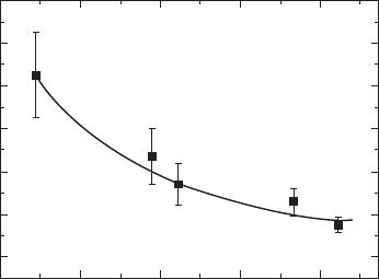
of the axis between a and b in the a–b plane. The strain energy is roughly
proportional to spontaneous deformation (S) expressed by S = a/b – 1. With
increasing La content (x), S decreases almost linearly from 0.007 (BiT) to
0.000 for BLT(x = 1.50), and orthorhombic distortion becomes smaller. The
close relation between S and the domain width of striped 90° domains is
revealed (see Fig. 33.14), and a smaller S results in a narrower domain
width, as can be clearly seen in Fig. 33.13. When S is lowered, the strain
energy density of domain walls decreases. Thus, this increases the density of
S
(= 1 –
a
/
b
)
0.0000.0020.0040.0060.008
90° domain width (mm)
12
10
8
6
4
2
0
BLT (
x
= 1.46)
BLT
(
x
= 0.85)
BLT
(
x
= 1.2)
BLT
(
x
= 0.46)
BiT
33.14
90° domain width as a function of spontaneous deformation
(
S
). The value of
S
is calculated from the structural data obtained by
the neutron diffraction Rietveld analysis.
WPNL2204
Crystal structure and defect control 1023
90° domain walls to attain a lower total energy. It can be said that S governs
90° domain structure in the a–b plane. However, the formation of ADB has
generally no relation to strain energy, and S does not affect the configuration
of ADB directly. Thus, we should consider local lattice distortion to elucidate
the nature of ADB.
Neutron diffraction study has revealed that La substitution leads to a
structural change in TiO
6
distortion along the b-axis as well as in the ferroelectric
distortion along the a-axis. While cooperative ionic displacements along the
a-axis result in the P
s
, the local dipole moments along the b-axis cancel each
other owing to the presence of glide plane. Now the TiO
6
rotation is focused
as a reference of local lattice distortion. BiT has two kinds of TiO
6
octahedron
as shown in Fig. 33.1; one is the octahedron at the middle of the perovskite
blocks (Ti1O
6
) and the other is the octahedron near Bi
2
O
2
layers (Ti2O
6
).
Here, only the octahedral distortion of Ti2O
6
is considered for simplicity.
For BiT, Ti2O
6
rotates by 8.7° around the a-axis in the b–c plane, while the
rotation angle around the b-axis in the a–c plane is only 2.4°. This indicates
that the local TiO
6
distortion is much larger in the b–c plane than that in the
a–c plane. La substitution causes a smaller TiO
6
rotation, and the rotation
angle for BLT (x = 0.75) is 8.2° in the b–c plane and 1.6° in the a–c plane.
In the single domain region, the phase of TiO
6
rotation is opposite for
adjacent octahedra that share oxide ions. The regular TiO
6
rotation does not
hold true at ADB, and the phase shift occurs by [1/2 1/2 0]. This irregular
TiO
6
rotation results in a large strain at ADB, and the strain energy becomes
less for a smaller TiO
6
rotation angle. The smaller TiO
6
distortion for BLT
seems to be a partial reason for the formation of ADB. The 90° domain
structure surrounded by ADB strongly suggests that the 90° domain is
constructed from ADB and the ADB acts as a nucleus of a new 90° domain,
as suggested by Ding et al. [30]. However, the formation of ADB as well as
90° domain is closely related to the phase transition from parent tetragonal
I4/mmm structure. Further study on the phase transition of BLT is required
to clarify the domain structure and its role in polarization switching.
33.6 Leakage current
The impedance spectroscopic analysis has shown that h
•
is the dominant
carrier for BiT crystals at relatively low temperatures [19]. During cooling
or annealing at intermediate temperatures, the crystals absorb oxygen into
the lattice, and the oxide ion occupies
V
O1
••
with the formation of h
•
according
to the following reaction:
1/2O V O + 2
2O1
O1
••
•
→
x
h
33.3
It has been reported that hole conduction becomes predominant over oxide-
ion conduction at relatively low temperatures [19]. It is reasonable to consider
WPNL2204
Handbook of dielectric, piezoelectric and ferroelectric materials1024
that hole conduction plays a detrimental role in leakage current at room
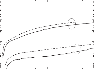
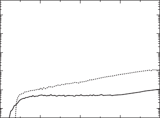
temperature. Figure 33.15 shows the leakage current (J) as a function of
electric field applied along the a-axis of the poled BiT crystals. For the
crystals grown in air, the ones annealed at 700°C in air had a relatively high
J of the order of 10
–7
to 10
–6
A/cm
2
. Note that annealing at 700°C under a
high
P
O
2
(35MPa) atmosphere resulted in a higher J in spite of reducing
oxygen vacancies. These results provide direct evidence that h
•
arising from
oxygen absorption is the dominant carrier for leakage current and hence
plays a detrimental role in the insulating properties of the BiT crystals at
room temperature.
Surprisingly, crystals grown in O
2
atmosphere (O
2
crystals) exhibit a
significantly lower J of the order of 10
–9
A/cm
2
, which is consistent with the
results of La-substituted BiT thin films [49].
As described above, heat treatment
at high temperatures inevitably creates
V
O1
••
as well as
′′′
V
Bi1
in the BiT lattice.
Crystal growth under a higher
P
O
2
atmosphere suppresses the defect formation,
and the O
2
crystals have a smaller number of these vacancies compared with
those grown in air. High-
P
O
2
annealing (700°C, 35MPa) also increases J of
the O
2
crystals. This increase in J shows that the vacancies are present even
in the O
2
crystals; a further defect control could lead to a lower J in the BiT
system.
Figure 33.16 shows the leakage current properties of BLT (x = 0.46)
crystals along the a-axis. The BLT crystals were grown in air. Note that BLT
(x = 0.46) crystals annealed in air at 700°C showed an extremely low J of the
order of 10
–9
A/cm
2
. The high-pressure oxygen annealing (
P
O
2
= 35 MPa) at
E
(kV/cm)
806040200
J
(A/cm
2
)
10
–9
10
–8
10
–7
10
–6
10
–5
10
–4
Grown in air
Grown in O
2
25°C,
E
ll
a
-axis
Annealed in air
Annealed in air
Annealed at
high
P
O
2
Annealed at
high
P
O
2
33.15
Leakage current density (
J
) as a function of electric field (
E
)
applied along the
a
-axis at 25°C for the BiT crystals grown in air and
O
2
atmosphere. The annealing at 700 °C under a high
P
O
2
of 35MPa
led to an increase in
J
.
WPNL2204
Crystal structure and defect control 1025
700°C increases J. Even though the oxygen annealing indeed decreases
V
O1
••
, the annealed crystals have a higher J. The oxygen annealing did not
change the metal composition of the crystals. The fact of the high J caused
by the oxygen annealing shows that the incorporation of oxygen into the
lattice caused by the annealing generates h
•
, as expressed by Eq. (33.3). It is
concluded that h
•
is the detrimental carrier in BLT crystals. The concentration
of h
•
is determined by the excess oxygen that is absorbed from the ambient
during annealing or cooling [19]. The La substitution reduces
V
O1
••
in the
perovskite layers owing to the high chemical stability of oxide ions near La
in the perovskite layers, and thus decreases h
•
. The chemical stabilization of
oxide ions by La substitution is the origin of the high insulating property
observed for the BLT crystals.
33.7 Polarization properties
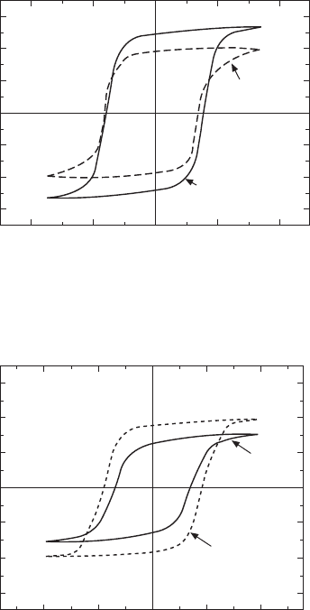
Figure 33.17 shows the polarization hysteresis loops of the BiT crystals with
air annealing (700°C, 5h) along the a(b)-axis. The air-grown crystals exhibit
a P
r
of 37µC/cm
2
and a coercive field (E
c
) of 35–40kV/cm. This P
r
value is
lower than those given in the previous reports [4, 5]. The O
2
crystals consistently
show a larger P
r
of 48µC/cm
2
. It is well known that a small P
r
of BiT
ceramics and thin films is a result of domain pinning caused by oxygen
vacancies [11, 50]. The improvement of P
r
observed for the O
2
crystals is a
result of domain depinning due to fewer
V
O1
••
associated with the high insulating
property.
Figure 33.18 shows the polarization hysteresis loops of the BLT (x = 0.46)
crystals at 25°C. The high-
P
O
2
annealing (
P
O
2
= 35MPa, 700°C, 10h)
E
(kV/cm)
806040200
J
(A/cm
2
)
10
–9
10
–8
10
–7
10
–6
10
–5
10
–4
Annealed in air
Annealed at
high
P
O
2
BLT (
x
= 0.46)
25°C,
E
ll
a
-axis
Grown in air
33.16
Leakage current density (
J
) as a function of electric field (
E
)
applied along the
a
-axis at 25°C for Bi
4–
x
La
x
Ti
3
O
12
(BLT,
x
= 0.46)
crystals. The annealing at 700°C under a high
P
O
2
of 35 MPa led to
an increase in
J
.
WPNL2204
Handbook of dielectric, piezoelectric and ferroelectric materials1026
improves the rectangularity of the hysteresis and increases P
r
from 25 to 36
µC/cm
2
. One of the reasons why the high-
P
O
2
annealing leads to the larger
P
r
is a weak pinning of domains for the annealed crystals due to the small
number of
V
O1
••
. The air-annealed crystals still have a certain amount of
V
O1
••
in the perovskite layers, and
V
O1
••
acts as a pinning center of the domain wall.
The oxygen annealing increases the number of switchable domains by applying
an electric field. The high-
P
O
2
annealing is demonstrated to be effective for
improving polarization properties in the BLT system with a high insulating
property.
E
(kV/cm)
–100 –50 0 50 100
P
(µC/cm
2
)
–60
–40
–20
0
20
40
60
25°C, 1Hz
E
ll
a
(
b
)-axis
Grown in O
2
(annealed in air)
Grown in air
(annealed in air)
33.17
Polarization hysteresis loops along the
a
-axis measured at
25 °C for the BiT crystals.
33.18
Polarization hysteresis loops along the a axis measured at
25°C for Bi
4–
x
La
x
Ti
3
O
12
(BLT,
x
= 0.46) crystals.
E
(kV/cm)
–100 –50 0 50 100
–60
–40
–20
0
20
40
60
P
(µC/cm
2
)
25°C, 1Hz
E
ll
a
(
b
) axis
grown in air
Annealed
at high
P
O
2
Annealed
in air
BLT
(
x
= 0.46)
WPNL2204
Crystal structure and defect control 1027
33.8 Effects of La and Nd substitutions on the
electronic band structure and chemical
bonding
The electronic structure of BNT (x = 2.0) was calculated for both the paraelectric
I4/mmm and the ferroelectric B2cb structures. The calculated band structure
of BNT (x = 2.0) near E
F
is almost the same as that of BiT (see Fig. 33.5a).
The calculation for the paraelectric BNT (x = 2.0) shows that the fundamental
E
g
is indirect (valence band maximum at P and conduction band minimum
at Γ), which is consistent with the result in the reported calculations [34]. In
contrast, our calculations suggest that the ferroelectric BNT (x = 2.0) has a
direct band gap, with the valence band maximum and conduction band
minimum lying at Brillouin-zone center Γ. Our calculation suggests that
BNT (x = 2.0) gives a narrower E
g(DFT)
of 2.4eV compared with BiT (E
g(DFT)
= 2.6eV), which is in good agreement with the results of the optical
measurements [35].
Figure 33.6(c) shows the total DOS between –25 and 7.5eV of BNT (x =
2.0) with B2cb ferroelectric structure. In this calculations, Nd is assumed to
occupy at the A site in the perovskite layers. The valence band consists
mainly of the O 2p states, while the Ti3d states form the conduction band.
The width of the valence band was approximately 5.5eV. Two kinds of Bi
for BiT result in two localized states of Bi 6s band near –10 eV, whereas
BNT has one peak of the Bi 6s band attributed to the Bi in the Bi
2
O
2
layers.
BiT and BNT indicate a similar low-lying O 2s band (–19 to –16eV), and the
broad Nd 5d states overlap with the O 2p band for BNT.
Figure 33.7(c) presents the PDOS of BNT (x = 2.0) with B2cb ferroelectric
structure. For both BiT and BNT, the Bi
2
O
2
layers show similar electronic
character, and the Bi2 and O2 in the Bi
2
O
2
layers do not have DOS near the
Fermi energy (E
F
). Thus, the perovskite layers play an essential role in the
electronic structure near the band gap, and E
g
is determined by the orbital
interaction in the perovskite layers. As in the case for BiT (see Fig. 33.7b),
the electronic structure of BNT shows that the valence band maximum mainly
consists of the O 2p orbitals. The conduction band minimum is composed of
the empty 3d orbitals of Ti in the perovskite layers. There is a strong
hybridization with Ti and Bi. This behavior reflects the strong hybridization
of the Ti3d and O2p orbitals in the perovskite layers, as is common for ABO
3
perovskites [51].
Interestingly, the Bi1 at the perovskite A site has a key role in the electronic
structure of the valence band for BiT. The antibonding orbitals are composed
of the 6s of the Bi1 and the 2p of the adjacent oxide ions form and constitute
the large DOS just below the E
F
. Furthermore, the orbital hybridization with
O2p leads to considerable DOS of the Bi1 6p states in the valence band. This
behavior is unexpected in a simplified ionic picture, but has been demonstrated
WPNL2204
Handbook of dielectric, piezoelectric and ferroelectric materials1028
also for α-PbO [52, 53], PbTiO
3
[51] and BiScO
3
-PbTiO
3
solid solution
[54]. The hybridization of the Bi1 6p-O 2p orbitals results in the bonding
states in the valence band, and the occupation of the Bi 6p electrons in the
valence band stabilizes the ferroelectric distortion in BiT.
Here, we discuss the role of Nd at the perovskite A site in view of electronic
structure and oxygen stability. The Nd 5d states found in the valence band is
a result of the orbital interaction with O 2p in the perovskite layers. Furthermore,
the substitution of Nd causes a significant change in DOS just below the E
F
.
The oxide ions in the perovskite layers (O1, O3, O5, O6) have a large DOS
near the E
F
in BiT, which are the antibonding states caused by the Bi1 6s–
O 2p hybridization. The Nd substitution decreases DOS near the E
F
due to
the lack of the Bi 6s–O 2p interaction and contributes to stabilizing the oxide
ions in the perovskite layers. The total/partial density of states (DOS) analysis
of BLT (x = 2.0) suggests that the La 5d is hybridized with the O 2p of the
adjacent oxygen. The covalent bonding between La and O in the perovskite
layers creates the DOS of the La 5d states in the valence band near the Fermi
level (–5~0eV), which is a possible origin of the high chemical stability of
oxygen in BLT.
Our calculations show that La and Nd substitutions at the perovskite A
site lead to a decrease in oxygen vacancy. The lower concentration of oxygen
vacancies is verified in BLT compared with BiT (see Fig. 33.10), which
originates from the orbital interaction between La and O in the perovskite
layers. The high stability of oxide ions are also expected for BNT, and this
is consistent with the results of a leakage-current density of the order of
10
–9
A/cm
2
of BNT crystals [35]. Compared with BiT, BLT and BNT crystals
exhibit a much lower leakage current, suggesting that defects such as oxygen
vacancies and electron holes are lower in the BLT and BNT crystals. It is
recognized that oxygen vacancies act as pinning site of domain wall and
impedes polarization switching [11, 50]. The suppression of domain pinning
results in a larger P
r
and high fatigue endurance, which have been achieved
for BNT thin films [24]. The results obtained in this study indicate that the
substitution of La and Nd is effective for stabilizing oxide ions in the perovskite
layers.
33.9 Summary
The crystal structures of Bi
4
Ti
3
O
12
in the ferroelectric and paraelectric states
have been analyzed, and the ferroelectric distortion has been discussed in
terms of ionic displacement of the constituent ions. The off-center Ti
displacements in TiO
6
octahedra play a minor role in spontaneous polarization,
while the entire shift of the TiO
6
octahedra with respect to heavy Bi ions
results in a large spontaneous polarization along the a-axis. The bond valence
analysis shows that the underbondings of Bi1 at the A site and Bi2 in the
WPNL2204
Crystal structure and defect control 1029
Bi
2
O
2
layers in the paraelectric state at 700°C is recovered to the satisfactory
bonding by the ferroelectric transition. The analysis of partial density of
states indicates that the ferroelectric transition originates from a strong
hybridization between the Bi1 6s(p) and the O3 2p states.
The defect structure and the mechanism of leakage current at room
temperature of Bi
4
Ti
3
O
12
, and the role of La and Nb in Bi
4
Ti
3
O
12
on the
ferroelectric-related properties are discussed. La and Nd substations at the
perovskite A site improve the chemical stability of the adjacent oxide ions
and reduces the concentration of oxygen vacancies. The results of the leakage
current properties of the single crystals reveal that electron holes arising
from the incorporation of oxygen at oxygen vacancies in the perovskite
layers act as detrimental carriers for leakage current at room temperature in
the Bi
4
Ti
3
O
12
system. A high insulating property at room temperature was
obtained for the La- and Nb-substituted Bi
4
Ti
3
O
12
crystals as a result of the
small number of electron holes due to fewer oxygen vacancies.
The substitutions of La and Nd give rise to a smaller remanent polarization
compared with Bi
4
Ti
3
O
12
, which is in good qualitative agreement with the
spontaneous polarization estimated from the structural data determined by
neutron diffraction analysis. Electronic band structure calculations and the
optical transmission data show direct band gap for the ferroelectric phases in
the Bi
4
Ti
3
O
12
system. The analysis of the electronic density of states of RE-
substituted lattice indicates that the orbital interaction of the RE 5d and O 2p
states stabilizes oxide ions in the perovskite layers, which is consistent with
the much lower leakage current observed for the RE-substituted crystals.
The observations of domain structure show that striped 90° domain walls
as well as head-to-head and tail-to-tail 180° domain walls are present in the
Bi
4
Ti
3
O
12
and La-substituted crystals. The substitution of La leads to a marked
decrease in the 90° domain width. Piezoelectric-force microscope observations
reveal that the antiphase domain boundary is formed only for La-substituted
crystals. The antiphase domain boundary is suggested to play an important
role in the formation of 90° domains.
33.10 Future trends
La and Nd substitutions into Bi
4
Ti
3
O
12
are effective for improving chemical
stability of oxide ions in the perovskite layers and thereby the leakage current
is suppressed to a very low value of the order of ~10
–9
A/cm
2
. These
substitutions, however, lead to a marked decrease in spontaneous polarization,
and thus the superior leakage-current properties due to less oxygen vacancies
are achieved by sacrificing the spontaneous polarization of Bi
4
Ti
3
O
12
.
Here, a definite guide for achieving polarization switching as well as a
low leakage current is proposed for the Bi
4
Ti
3
O
12
-based devices. Although
the processing temperature of the Bi
4
Ti
3
O
12
films is about ~ 700°C which is
WPNL2204