Zuo-Guang. Ye Advanced Dielectric Piezoelectric and Ferroelectric Materials: Synthesis, Characterisation and Applications
Подождите немного. Документ загружается.

Handbook of dielectric, piezoelectric and ferroelectric materials980
Although the reactive MBE process produces perovskite superlattices of
the highest quality, the deposition rate of the MBE process is still too slow
to prepare perovskite superlattices for practical applications. Most of the
industrial manufacturing processes of oxide thin films are still by simple and
conventional RF-magnetron sputtering. Therefore, we tried to make BTO/
STO superlattices using a simple sputtering system as shown in Fig. 32.5(b).
A substrate is rotated with an air actuator to alternately face the RF-plasma
of BTO (A) and STO (B) targets. The thickness of each layer is determined
from the deposition time. Tsai et al.
25
prepared the BTO/STO superlattices
and Wu and Hung
27
made the PbZrO
3
/BaZrO
3
superlattices using RF-
magnetron sputtering systems. They confirmed the formation of superlattices
from the satellite peaks in XRD profiles. Although the RF-sputtering is a
promising process for practical applications, the quality of the superlattices
must be improved to obtain the desired properties.
32.3 Lattice distortions in artificial superlattices
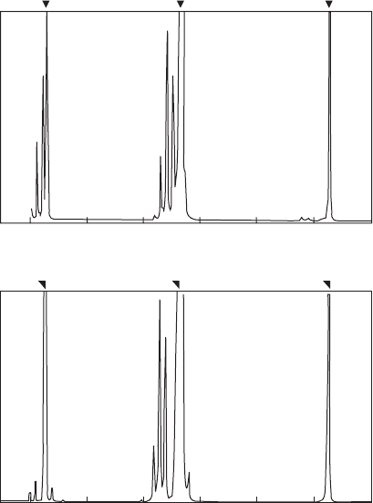
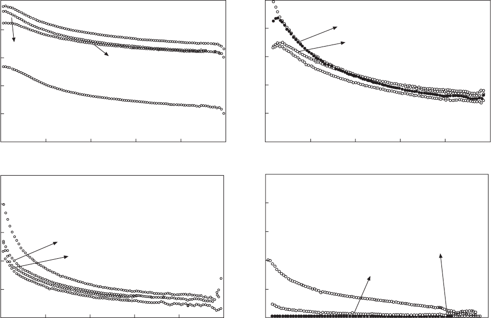
Figure 32.6 shows the XRD profiles of BTO/STO and SZO/STO superlattices
made with the MBE system shown in Fig. 32.2. Clear satellite peaks indicate
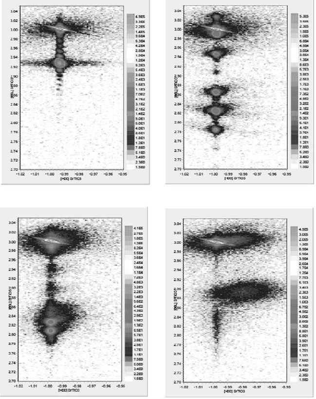
the formation of superlattices. XRD reciprocal-space-mapping measurements
were performed using high-resolution XRD equipment (Bruker AXS,
Discover8). Typical reciprocal-space-mappings obtained for BTO/STO
superlattices are shown in Fig. 32.7. The highest peaks in the maps are the
002 diffractions of the STO substrates. Clear satellite peaks are observed in
[BTO
10
/STO
10
]
4
superlattices. The shift of diffraction spots to the x-direction
(a*-axis) in the maps indicates that the a-parameter (in-plane lattice parameter)
of the epitaxial film changed from that of the substrate due to the relaxation
of crystal lattices. In [BTO
10
/STO
10
]
4
superlattices, all satellite peaks lie on
the same a* line as the substrate, indicating that the strained lattice is formed
in the films without relaxation of crystal lattices. In this case, a large lattice
distortion was induced by the lattice mismatch between BTO and STO in
substrate and in superlattices. On the other hand, a diffraction spot of the
[BTO
40
/STO
40
]
1
is shifted in the x-direction from the substrate by the relaxation
of crystal lattice.
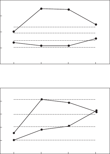
The variations of the a- and c-parameters with the periodicity of BTO/
STO and SZO/STO superlattices calculated from the diffraction angles of
002 peaks are shown in Fig. 32.8. It should be noted that all superlattices in
one series have the same total thickness (80 perovskite unit cells) and the
same chemical composition (Ba : Sr = 0.5 : 0.5 and Ti : Zr = 0.5 : 0.5). The
dotted lines in Fig. 32.8 indicate the lattice parameters of bulk samples. In
the case of BTO/STO superlattices, the a-parameters of superlattices with
the periodicities of 10 and 20 unit cells are identical to that of STO substrate,
indicating that almost completely strained lattices are formed in these
WPNL2204
Dielectric and optical properties of perovskite 981
superlattices. The a-parameter was relaxed to a large value when the periodicity
was increased to 40. The anisotropy of the crystal lattice has a maximum at
the periodicity of 10. On the other hand, the a-parameter of SZO/STO
superlattices increases with the periodicity. The c-parameter of the superlattice
with the periodicity of 10 is consistent with that of the ideally strained lattice
calculated from the unit cell volume of the bulk samples. The anisotropy of
the crystal lattice has the maximum value in this superlattice. The lattice
parameters of the superlattice with the periodicity of 40 are almost the same
as bulk SZO ceramics because the diffraction from the STO layer in the
relaxed superlattice is overlapped with that of the substrate and the lattice
parameters are calculated from the diffraction only from the SZO layer in the
superlattice.
The different behaviors in the variation of lattice parameters between
BTO/STO and SZO/STO superlattices in Fig. 32.8 are attributable to the
difference in the a-parameters of bulk samples of BTO
(0.3994 nm) and SZO
Substrate
Substrate
Intensity/Arb. unitsIntensity /Arb. units
CuKα 2θ/deg.
CuKα 2θ/deg.
70 806050403020
(a)
(b)
70 806050403020
32.6
XRD profiles of (a) [BTO
10
/STO
10
]
4
and (b) [SZO
10
/STO
10
]
4
superlattices.
WPNL2204
Handbook of dielectric, piezoelectric and ferroelectric materials982
(0.4100nm). As the SZO has a large a-parameter, the in-plane compressive
strain induced to the SZO layers from the STO substrate and the STO layers
in the superlattices cannot be retained with the increase of the periodicity,
giving rise to the relaxation of lattice strains, more easily than the case of
BTO/STO superlattices. The lattice parameters of the superlattices with a
periodicity of 1 have anomalous values, i.e. the c-parameters of the superlattices
markedly shrink in both cases. The formation of solid solution films due to
(a) [BTO
1
/STO
1
]
40
(b) [BTO
10
/STO
10
]
4
(c) [BTO
20
/STO
20
]
2
(d) [BTO
40
/STO
40
]
1
32.7
XRD reciprocal-space-mappings of BTO/STO superlattices.
WPNL2204
Dielectric and optical properties of perovskite 983
the interdiffusion of constituent elements is the reason for this phenomenon
but the lattice volume shrinkage observed in the SZO/STO superlattice cannot
be explained at present.
32.4 Optical property of artificial superlattices
32.4.1 Spectroscopic ellipsometry
Ellipsometry is an optical technique that can evaluate the optical constant
and film thickness of a thin film simultaneously. It is widely used for the
characterization of thin films and in-situ observation of growth process of
thin films.
41–46
The basic theory of ellipsometry was summarized in a book
written by Azzam and Bashara.
47
There are some reports on the ellipsometry
of semiconductor superlattices
48–52
but the studies on oxide artificial
superlattices are extremely limited except for our work on NiO/ZnO
superlattices prepared by the IBS process.
53
32.8
Variations of lattice parameters with the stacking periodicity of
(a) BTO/STO superlattices and (b) SZO/STO superlattices.
Identically strained
Stacking periodicity
(a)
4020101
Lattice parameter (nm)
0.42
0.41
0.40
0.39
0.38
Lattice parameter (nm)
0.43
0.42
0.41
0.40
0.39
0.38
Stacking periodicity
(b)
4020101
c
-axis
a
-axis
STO
BTO
c
-
a
-
Ba
0.5
Sr
0.5
TiO
3
c
-axis
a
-axis
STO
SZO
Sr(Ti
0.5
Zr
0.5
)O
3
WPNL2204
Handbook of dielectric, piezoelectric and ferroelectric materials984
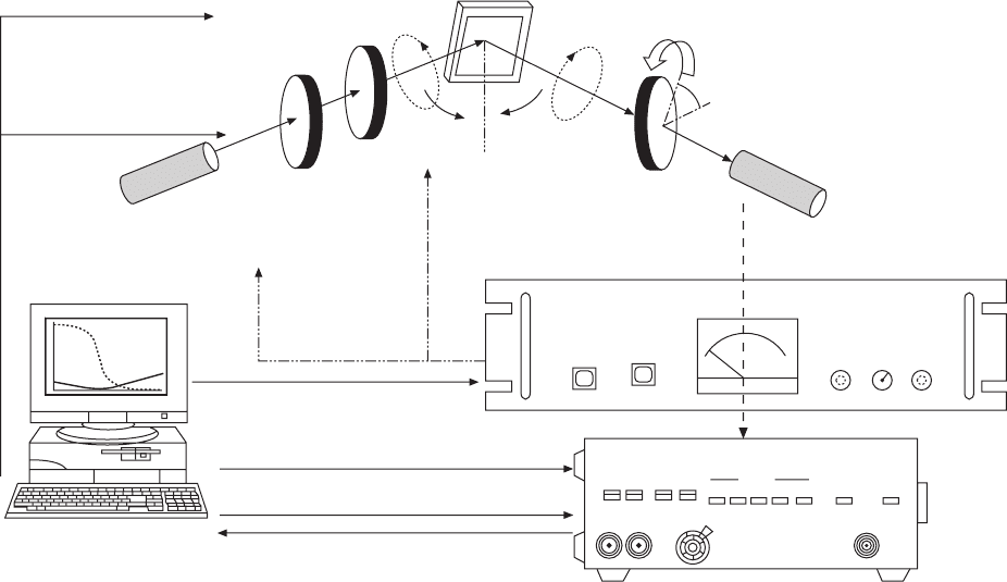
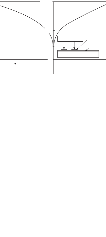
Figure 32.9 shows the rotating-analyzer type spectroscopic ellipsometer
used for the evaluation of ellipsometer angles, Ψ and ∆, of superlattices on
substrates. Reflection ellipsometry is a technique based on the measurements
of the states of polarization of the incident and reflected waves, leading to
the determination of the ratio ρ of the complex Fresnel reflection coefficients.
The ratio
ρ is represented in terms of ellipsometer angles by ρ = tan Ψ
exp(i∆). The rotation-analyzer ellipsometer becomes inaccurate when ∆ <
10° or ∆ > 170°
54
which is frequently encountered in the measurements of
transparent films.
55–58
To avoid this problem, a compensator (a quarter-wave
retarder) is inserted after the polarizer to change the polarizing state of
incident light. Polarized light from 350 to 850 nm in wavelength is provided
from a Xe lamp (75 W) through a computer-controlled monochrometer and
an optical fiber. The incident angle is varied from 50° to 80°. The refractive
indices of thin films were calculated using the three-phase model (ambient
thin films substrate). In the analysis, the superlattices were regarded as uniform
thin films along the thickness. The difficulty in the ellipsometric measurements
of superlattices is that the refractive index of the substrate is very close to
that of thin films. We measured the ellipsometer angles of STO substrates
very accurately to prepare database used for the analysis of thin films. Nonlinear
least-squares-fitting software was developed to determine the optical constant,
n* = n – iκ, where n is the refractive index and κ is the extinction coefficient,
from the complex Fresnel reflection coefficients (ρ) determined at different
incident angles. No theoretical assumption was used to evaluate the wavelength
dispersion of refractive index.
32.4.2 Optical constants of superlattices
The refractive index (n) and extinction coefficient (κ) of the BTO/STO and
SZO/STO superlattices determined by the ellipsometer system are shown in
Fig. 32.10 as a function of light wavelength. The refractive index decreases
with increasing wavelength for all specimens. High refractive indices at low
wavelengths are due to the effect of the fundamental absorption below
350nm. It was found that the BTO/STO and SZO/STO superlattices with the
periodicity of 10 had higher refractive indices than those of the other
superlattices over the whole wavelength range. The variation of refractive
index at a wavelength of 500nm with the stacking periodicity of the superlattices
is shown in Fig. 32.11. The refractive index shows a maximum at the periodicity
of 10 in both systems. The superlattices with a periodicity of 10 had the
highest anisotropy of crystal lattice as shown in Fig. 32.8. The result in Fig.
32.11 indicates that the lattice distortions induced by the lattice mismatches
change the electronic states affecting electronic polarizations in the superlattices,
giving rise to the variation of refractive index even though the averaged
chemical compositions of the superlattices are identical.
WPNL2204
Dielectric and optical properties of perovskite 985
DIO
Ellipsometry
control computer
A/D (data)
D/A (offset)
DIO (gain control)
GPIB
Incident angle
control
Wavelength
control
Light source
monochromator
Shutter & filter
control
Polarizer
Compensator
Sample
Θ
0
Θ
0
Analyzer
Detector
Signal
Analogue controller
Level
Offset
Meas
Power
Differential amplifier
Gan
GanMatInroads
Input
Output
Power
Radio
width
Offset
Input
32.9
Schematic illustration of rotating-analyzer type spectroscopic ellipsometer.
WPNL2204
Handbook of dielectric, piezoelectric and ferroelectric materials986
Wavelength (nm)
450350 550 650 750 850
Wavelength (nm)
450350 550 650 750 850
(b)
0.50
0.40
0.30
0.20
0.10
0.00
Extinction coefficient (κ)
[SZO
10
/STO
10
]
4
[SZO
20
/STO
20
]
2
[SZO
1
/STO
1
]
40
[SZO
40
/STO
40
]
1
Refractive index (
n
)
2.5
2.4
2.3
2.2
2.1
2.0
[SZO
40
/STO
40
]
1
[SZO
1
/STO
1
]
40
[SZO
20
/STO
20
]
2
[SZO
10
/STO
10
]
4
Wavelength (nm)
(a)
850750650550450350
Wavelength (nm)
850750650550450350
Extinction coefficient (κ)
0.25
0.20
0.15
0.10
0.05
0.00
Refractive index (
n
)
2.5
2.3
2.1
1.9
1.7
1.5
[BTO
10
/STO
10
]
4
[BTO
1
/STO
1
]
40
[BTO
20
/STO
20
]
2
[BTO
40
/STO
40
]
1
[BTO
40
/STO
40
]
1
[BTO
20
/STO
20
]
2
[BTO
10
/STO
10
]
4
[BTO
1
/STO
1
]
40
32.10
Optical constant of (a) BTO/STO and (b) SZO/STO superlattices as a function of wavelength.
WPNL2204
Dielectric and optical properties of perovskite 987
32.5 Dielectric properties of artificial superlattices
32.5.1 Electrodes and measuring principle and technique
The selection of substrate is extremely important for the growth of perovskite
superlattices. The (001)-oriented STO single crystal is frequently used for
the substrate of superlattice growth because of its high crystallinity and a
small lattice mismatch with perovskite films. However, for the electric
measurements, superlattices should be deposited on a conductive layer working
as a bottom electrode. The easiest way to meet this demand is the usage of
conductive Nb-doped STO single crystals. We have used this substrate at the
beginning of the research but it gave a serious problem of high leakage
current in the superlattices. Figure 32.12 shows the difference in the leakage
currents between the BTO/STO superlattices deposited on undoped STO and
on Nb-doped STO substrate. The leakage current was measured between two
neighboring electrodes of In on the film surface as shown in the drawing in
Fig. 32.12. The In electrode makes an ohmic contact with semiconductive
oxides. The superlattice deposited on the Nb-doped STO substrate showed a
Stacking periodicity
(a)
403020101
Refractive index (
n
)
2.4
2.3
2.2
2.1
2.0
1.9
Stacking periodicity
(b)
Refractive index (
n
)
2.27
2.26
2.25
2.24
2.23
2.22
403020101
32.11
Refractive index of (a) BTO/STO and (b) SZO/STO superlattices
measured at wavelength of 500nm.
WPNL2204
Handbook of dielectric, piezoelectric and ferroelectric materials988
higher leakage current although the substrate was not used as a bottom
electrode. On the other hand, the leakage current of the superlattice on
undoped STO was lower than the measuring limit of the electric current
meter used for the measurement. The high leakage current observed in the
superlattice on the the Nb-doped STO substrate could not be improved by
annealing films in oxygen atmosphere or variation of the stoichiometry of
the films. We believe that the high leakage current is due to the thermal
diffusion of Nb into the film. It may be that some of anomalous dielectric
behaviors reported for artificial superlattices on the Nb-doped STO substrates
may be due to the Maxwell–Wagner polarization between electrodes with
the Schottky barrier.
To avoid the problem of the high leakage current mentioned above, we
tried to measure the dielectric properties of the superlattices on undoped
STO using planar electrodes on the film. Farnell’s theory
59
is frequently
used to evaluate the dielectric permittivity of films measured with interdigital
electrodes. From this theory, the relation between the dielectric permittivity
of a substance and the capacitance measured with interdigital electrodes is
given by:
C
l
= K(ε
s
+ 1)
K
D
L
D
L
= 6.5 + 1.08 + 2.37
2
() ()
32.1
where C
l
is the capacitance per unit length, ε
s
is the dielectric permittivity of
the substance, D is the width of the finger and L is the distance between the
center of two neighboring fingers in interdigital electrodes. The capacitance
Voltage (V)
Electric current (nA)
0–0.5–1.0 0.5 1.0
On undoped STO
On Nb-doped
STO
10000
100000
1000
100
10
Substrate
Thin film
Top
electrode
(In)
Micro-prober
32.12
Leakage current of BTO/STO superlattices on STO and Nb-
doped STO substrate.
WPNL2204
Dielectric and optical properties of perovskite 989
of a film on a substrate (C) is represented by the capacitance due to the film
C
F
and that due to the substrate C
S
as follows:
C = C
S
+ (C
F
– C
S
)[1 – exp(–4.6h/L)] 32.2
where h is the thickness of film. By combining Eqs. (32.1) and (32.2), the
dielectric permittivity of the film is calculated from the capacitances C and
the permittivity of the substrate ε
s
. However, Eqs. (32.1) and (32.2) are
accurate only under the conditions that the permittivity of substrate and film
is 50 or less, the finger width D and the space between fingers (L – D) are
equal and the ratio of the film thickness h to the space between fingers
(D – L) is 0.2 or more. These conditions cannot be satisfied in the case of
superlattices with a thickness of about 32nm (80 unit cells of the primitive
perovskite lattice). Therefore, electromagnetic (EM) field analysis (Sonnet,
EM) was employed to calculate the film permittivity from the capacitance
measured with interdigital electrodes. The validity of Farnell’s theory was
simulated at first. The parameters used for the simulation are as follows: the
dielectric permittivity of the substrate is 300 (STO), the film thickness (h) is
32nm, the finger-to-space ratio D/(L – D) is fixed at 0.5 and the finger width
D is changed from 5 to 50µm. The thickness of the substrates and that of the
air above the electrode were 0.5 mm and 10mm, respectively. The results of
the simulation using Farnell’s theory and the EM analysis are compared in
Fig. 32.13 where the capacitance is normalized to that simulated for the
substrate without film. The normalized capacitance increases with decreasing
finger width D in both Farnell’s theory and the EM analysis. Although
Farnell’s theory gave a relatively good approximation when the film permittivity
was low, the capacitance calculated from Farnell’s theory became higher
than that from the EM analysis as the dielectric permittivity of the film
increased. This result indicates that Farnell’s theory overestimates the
permittivity of ultra-thin superlattices and that the EM analysis is indispensable
to determine the dielectric permittivity of the superlattices with high dielectric
permittivity.
The required finger width of interdigital electrodes for the measurements
of superlattices was determined using EM analysis. In this analysis, the
admittance calculated for a substrate (ε
s
= 300) was compared with that
calculated for the substrate with a film (30nm, ε = 1000). The ∆Y defined by
∆Y = (Y
t
– Y
s
)/Y
t
, where Y
s
is the admittance of the substrate and Y
t
is the
admittance of the film and the substrate, is shown in Fig. 32.14 as a function
of the finger width of interdigital electrodes. The ∆Y increases with decreasing
finger width, indicating that the contribution of the film to the admittance
increases with decreasing finger width. The result in Fig. 32.14 shows that
the finger width of interdigital electrodes should be less than 10µm to obtain
reliable admittance data of the film. Based on this analysis, the finger width
was determined to be 5 µm in the final design and the simulation model as
shown in Fig. 32.15.
WPNL2204