Nof S.Y. Springer Handbook of Automation
Подождите немного. Документ загружается.

Nanomanufacturing Automation 53.2 AFM-Based Nanomanufacturing 935
When the alternating pushing forces at two points
on the nanowire are applied, a nanowire rotates around
two pivots P
i
and Q
i
. The distance L
1
between P
i
and
Q
i
can be calculated if the pushing points are deter-
mined. The two pivots P
s
and P
d
are connected to form
a straightline, and thedistance d between thetwo points
is calculated. d is then divided into N small segments
(the numberof manipulations). Then L
p
in Fig.53.9 can
be obtained
L
p
=
d
N
, 0 < L
p
< 2L
1
. (53.24)
During manipulation, the pivot P
i
is always on the line
generated by the two points P
s
and P
d
. Then the rotation
angle for each step can be obtained
θ =2acos
L
p
2L
1
.
(53.25)
The rotation angle θ stays the same during manipu-
lation. The initial pushing angle θ
1
and the final pushing
angle θ
2
in Fig.53.9 can be calculated by finding the
starting position and the ending position. After θ is de-
termined, the pivots P
i
and Q
i
(i = 1,...,N) can be
calculated. The pushing points can then be determined.
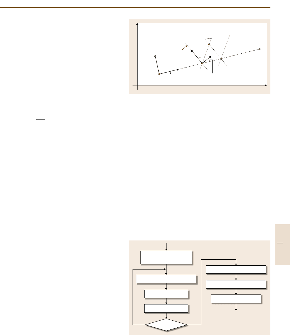
Here we show how to determine the pushing points
when a nanowire rotates around the pivot P
i
as an ex-
ample. Figure53.10 shows the frames used to determine
the tip position.
The following transformation matrix can be easily
calculated. The transformation matrix of the frame orig-
inated at P
s
relative to the original frame is T
s
. The
transformation matrix of the frame originated at P
i
rel-
ative to the frame originated at P
s
is T
i
. Supposing the
rotation angle is β(0 <β≤θ), the transformation ma-
trix relative to the frame originated at P
i
is T
βi
. β can
be obtained by setting a manipulation step size. The
coordinates of the pushing point can then be calculated
⎛
⎜
⎝
X
F
Y
F
1
⎞
⎟
⎠
=T
s
T
i
T
βi
⎛
⎜
⎝
0
L −2s
1
⎞
⎟
⎠
.
(53.26)
Similar steps can be followed to determine the pushing
position for a nanowire rotating around the pivot Q
i
, i ∈
[1, N]. After the coordinates of the pushing point are
obtained, the manipulation path for a nanowire can be
generated.
53.2.3 Automated Local Scanning Method
for Nanomanipulation Automation
The random drift due to thermal extension or contrac-
tion causes a major problem during nanomanipulation,
θ
θ/2
α
θ
F
P
i+1
P
i
P
s
O
y
x
P
d
y
i
y
s
x
i
x
s
Q
i
Fig. 53.10 The coordinates used to compute the AFM tip pushing
position at each step
because the object may be easily lost or manipulated
to wrong destinations. Before the manipulation, the ob-
jects on the surface are identified and their positions are
labeled. However, the labeled positions of the nanoob-
jects have errors due to random drift. To compensate for
the random drift, the actual position of each nanoob-
ject must be identified before each operation. Because
the time to scan a big area is quite long, a quick local
scanning mechanism is developed to obtain the actual
position of each nanoobject in a short time. Nanoma-
nipulation is then performed immediately after the local
scan. Figure 53.11 shows the local scanning method.
From the path data, the original position of
a nanoobject is obtained. Also, the nanoobject is cate-
gorized into two groups: the nanoparticle and nanowire.
A scanning pattern is generated for the nanoobject ac-
cording to its group. The scanning pattern is fed to the
imaging interface to scan the surface. If the nanoob-
Original object position
and categorization
Scanning pattern generation
Imaging interface
Line scan
Perpendicular line scan
Actual position computation
Path adjustment
Object found?
New path
Path
YesNo
Fig. 53.11 The local scanning strategy to obtain the actual positions
of nanoobjects
Part F 53.2
936 Part F Industrial Automation
L
2
L
0
L
1
P
2
P
1
Q
1
Q
2
O
a
V
O
R
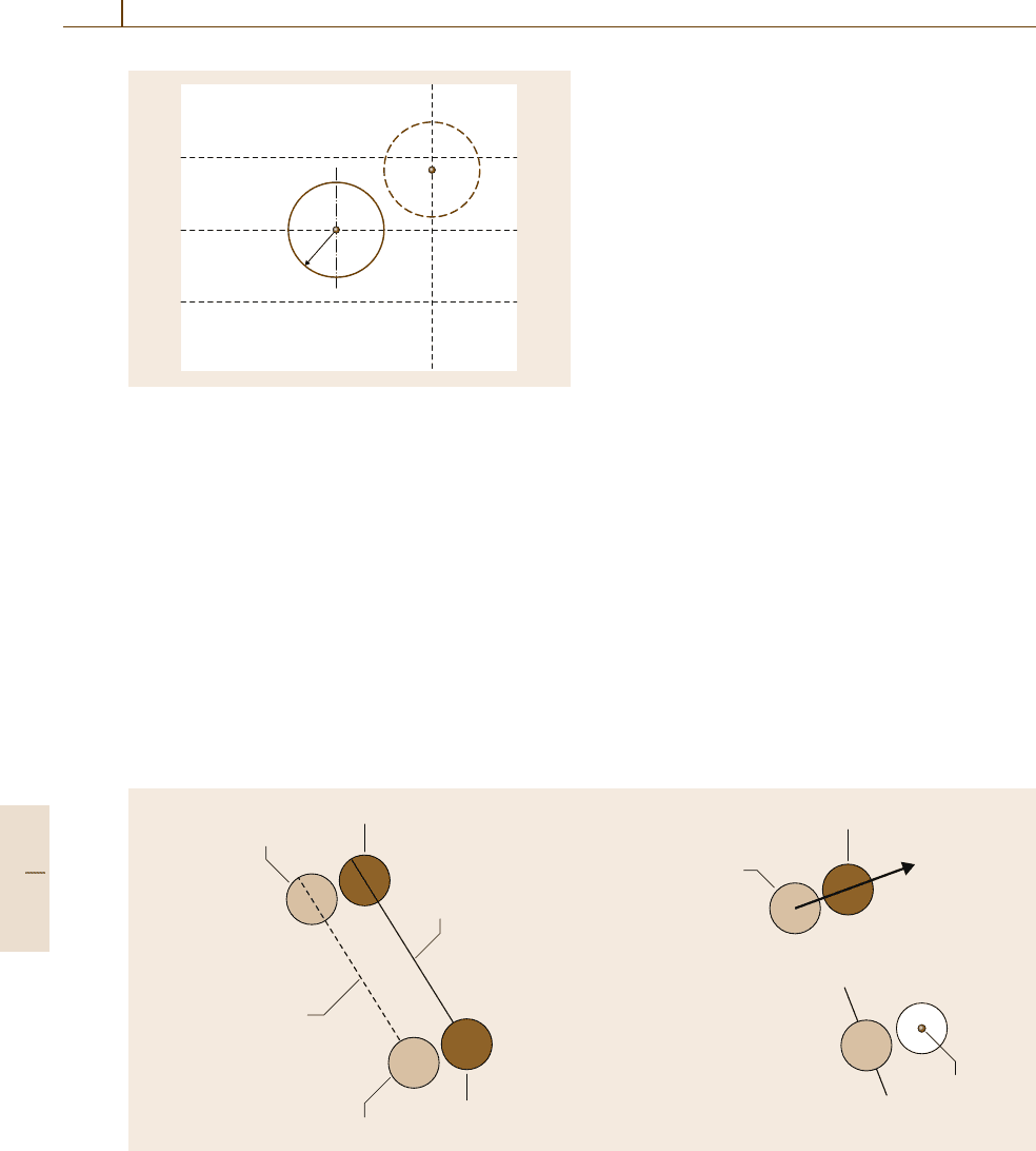
Fig. 53.12 Local scan pattern to search the actual position
of a nanoparticle. O is the original center of the particle,
R is the radius of the particle, O
a
is the actual center of
the particle, L
0
,L
1
,andL
2
are the horizontal scan lines,
V is the vertical scan line. P
1
and P
2
are the interactions
between the particle edge and a horizontal scan line, Q
1
and Q
2
are the intersections between the particle edge and
the vertical scan line
ject is not found, a new scanning pattern is generated.
The process continues until the nanoobject is discov-
ered. The actual position of the nanoobject can then be
computed. Themanipulation pathis then adjusted based
on the actual position. For nanoparticles and nanoob-
jects, different scanning patterns must be used in order
to obtain their actual position.
New position
Actual position
Original position
Drift direction
First point
New destination
Original destination
Original position
a) b)
New path
Original path
Fig. 53.13 (a) The updated path after drift compensation. (b) The local scan after the drift direction and size are
determined from the previous local scan
For example, the location of a nanoparticle can be
represented by its center and radius. The radius of each
particle R has been identified before the manipulation
starts. The actual center of a nanoparticle can be relo-
cated by two lines, a lateral and a cross line as shown
in Fig.53.12. First, the nanoparticle is scanned using
line L
0
, which passes the original center of the par-
ticle in the image. If the particle is not found, then
the scanning line moves up and down alternatively by
a distance of 3/2R. Once the particle has been found,
two intersection points, P
1
and P
2
between the particle
edge and the lateral line are located. A cross line scan
V, which goes through the middle point between P
1
and P
2
, is used to locate the center of the particle. The
cross scan line has two intersection points, Q
1
and Q
2
,
with the particle edge. The middle point between Q
1
and Q
2
is the actual center of the nanoparticle. The lo-
cal scanning range (the length of the scanning line) l
can be determine by the maximum random drift such
that l > R+r
max
, wherer
max
is the estimated maximum
random drift distance.
After the center of a nanoobject has been identified,
the drifts in the XY directions are calculated. The drifts
in the XY directions are then used to update the desti-
nation position as shown in Fig.53.13a. Finally a new
path is generated to manipulate the nanoparticle.
After the local scan of the first nanoparticle, the
direction and size of the drift can be estimated. The in-
formation can be used to generate the scanning pattern
for the next nanoobject as shown in Fig.53.13b.
Part F 53.2
Nanomanufacturing Automation 53.3 Nanomanufacturing Processes 937
53.2.4 CAD Guided Automated
Nanoassembly
In order to increase the efficiency and accuracy of
AFM-based nanoassembly, automated CAD guided
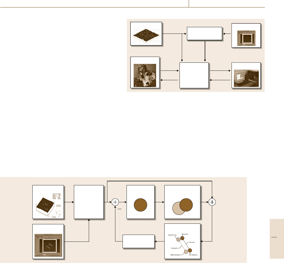
nanoassembly is desirable. A general framework for
automated nanoassembly is developed to manufac-
ture nanostructures and nanodevices, as illustrated
in Fig.53.14. Based on the CAD model of a nanostruc-
ture and the distribution of nanoobjects on a surface
from an AFM image, the tip path planner generates
manipulation paths to manipulate the nanoobjects. The
paths arefed to a user interface to simulate the manufac-
turing process and then to the AFM system to perform
the nanoassembly process.
The AFM tip path planner is the core of the gen-
eral framework. Figure 53.15 shows the architecture of
the tip path planner. Nanoobjects on a surface are first
identified based on the AFM image. A nanostructure
is then designed using the available nanoobjects. Ini-
tial collision-free manipulation paths are then generated
based on the CAD model of a designed nanostruc-
ture. In order to overcome the random drift, a local
scanning method is applied to identify the actual po-
Automated
manipulation
Actual positionLocal scanAFM image
CAD model
Automated
path
generation
Updated path
Fig. 53.15 Automated tip path planner. Initial paths are generated based on the CAD model of a designed nanostructure
and the randomly distributed nanoobjects on a surface. The manipulation path of each nanoobject is adjusted accordingly
based on the local scanning result
Automated tip
path planner
Simulation
and
real-time
operation
General paths
Real-time
display
Interface
CAD model
AFM image
AFM
Commands
Force
Control
Fig. 53.14 The general framework for automated path generation
system. The bottom left is the AFM system and the bottom right
is the augmented reality interface used for simulation and real-time
operation
sition of a nanoobject before its manipulation. Each
manipulation path of the nanoobject is adjusted ac-
cordingly based on its actual position. The regenerated
path is then sent to the AFM system to manipu-
late the nanoobject. The process continues until all
nanoobjects are processed. A nanostructure is finally
fabricated.
53.3 Nanomanufacturing Processes
The nanomanufacturing process for nanodevices is not
straightforward, especially in nanomaterial preparation,
selection, and deposition processes. To prepare the
nanomaterial, nanoobjects are usually dissolved into
solution, then the nanoobject suspension is put in an
ultrasonicator or a centrifuge for dispersing the nanoob-
jects. Afterwards, specific properties of the nanoobjects
should be selected. Finally, they are delivered to as-
Part F 53.3
938 Part F Industrial Automation
semble the nanodevices. However, the nanoobjects are
too small to be manipulated by traditional robotic sys-
tems, novel devices and systems must be developed for
this. Since the nanoobjects are dissolved into fluids,
dielectrophoresis and microfluidic technology can be
considered to perform the tasks. The material prepara-
tion can be done by micromixers; the selection process
can be done by microfilters; and the deposition process
can be done by integrating the microchannel and mi-
croactive nozzle to deposit the nanoobject suspension.
CNT is one of the most common nanoobjects and it
has some promising properties that are useful for gen-
eration nanodevices. In this chapter, the development
of a novel automated CNT separation system to clas-
sify the electronic types of CNTs will be described,
which involves the analysis for DEP force on CNTs
and fabrication of a DEP microchamber. Moreover,
this DEP microchamber was successfully integrated
into an automated deposition workstation to manipulate
a single CNT to multiple pairs of microelectrodes re-
peatedly. The automated deposition processes for both
SWCNTsandMWCNTs will be presented. As a result,
CNT-based nanodevices with specific and consistent
electronic properties can be manufactured automati-
cally. The resulting devices can potentially be used in
commercial applications.
53.3.1 Dielectrophoretic Force
on Nanoobjects
Dielectrophoresis has been used to manipulate and sep-
arate different types of biological cells. DEP forces
can be combined with field-flow fractionation for si-
multaneous separation and measurement [53.46]. DEP
force induces movement of a particle or a nanoobject
under non-uniform electric fields in liquid medium as
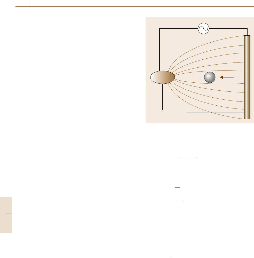
shown in Fig.53.16. The nanoobject is polarized when
it is subjected to an electric field. The movement of
the nanoobject depends on its polarization with respect
to the surrounding medium [53.47]. When the nanoob-
ject is more polarizable than the medium, a net dipole
is induced parallel to the electric field in the nanoob-
ject and, therefore, the nanoobject is attracted to the
high electric field region. On the contrary, an oppo-
site net dipole is induced when the nanoobject is less
polarizable than the medium, and the nanoobject is
repelled by the high electric field region. The direc-
tion of the DEP force on the particle is given by the
Clausius–Mossotti factor (CM factor, K). It is defined
as a complex factor, describing a relaxation in the effec-
tive permittivity of the particle with a relaxation time
Microelectrodes
Particle
F
DEP
Liquid medium
AC voltage
Nonuniform
electric field
Fig. 53.16 Illustration of the dielectrophoretic manipula-
tion
described by [53.47,48]
K(ε
∗
p
,ε
∗
m
) =
ε
∗
p
−ε
∗
m
ε
∗
p
+2ε
∗
m
. (53.27)
Complex permittivities of the nanoobject (ε
∗
p
)and
medium (ε
∗
m
) are defined and given by [53.47,48]
ε
∗
p
=ε
p
−i
σ
p
ω
,
(53.28)
ε
∗
m
=ε
m
−i
σ
m
ω
,
(53.29)
where ε
p
and ε
m
are the real permittivities of the
nanoobject and the medium, respectively, σ
p
and σ
m
are
the conductivities of the nanoobject and the medium, re-
spectively, and ω is the angular frequency of the applied
electric field; the CM factor is frequency-dependent.
The time-averaged DEP force acting on the particle is
given by [53.47,48]
F
DEP
=
1
2
Vε
m
Re(K)∇|E |
2
, (53.30)
where V is the volume of the nanoobject and ∇|E |
2
is
the root-mean-square of the applied electric field. Based
on this equation, the direction of the DEP force is de-
termined by the real part of the CM factor K.When
Re[K]> 0, the DEP force is positive, and therefore the
CNT is moved toward the microelectrode in the high
electric field region. When Re[K]< 0, the DEP force
Part F 53.3
Nanomanufacturing Automation 53.3 Nanomanufacturing Processes 939
is negative, the particle is repelled away from the mi-
croelectrode. Moreover, we know that the magnitude
and direction of DEP forces depends on the size and
material properties of the nanoobjects, so separation of
nanoobjects can be done.
53.3.2 Separating CNTs
by an Electronic Property
Using the Dielectrophoretic Effect
A theoretical analysis of DEP manipulation on a CNT
was performed, and CM factors were calculated for
a metallic SWCNT (m-SWCNT) and a semiconducting
MWCNTs(s-SWCNT), respectively. In the analy-
sis, semiconducting and metallic CNT mixtures are
dispersed in the alcohol medium assuming the permit-
tivities of a s-SWCNT and a m-SWCNT are 5ε
0
[53.32]
and 10
4
ε
0
[53.37], respectively, where ε
0
is the per-
mittivity of free space (ε
0
= 8.854188×10
−12
F/m).
The conductivities of a s-SWCNT and a m-SWCNT
are 10
5
S/m and 10
8
S/m [53.37], respectively. The
permittivity and conductivity of the alcohol are 20ε
0
and 0.13μS/m, respectively. Based on these parame-
ters and (53.27), plots of Re[K] for different CNTs
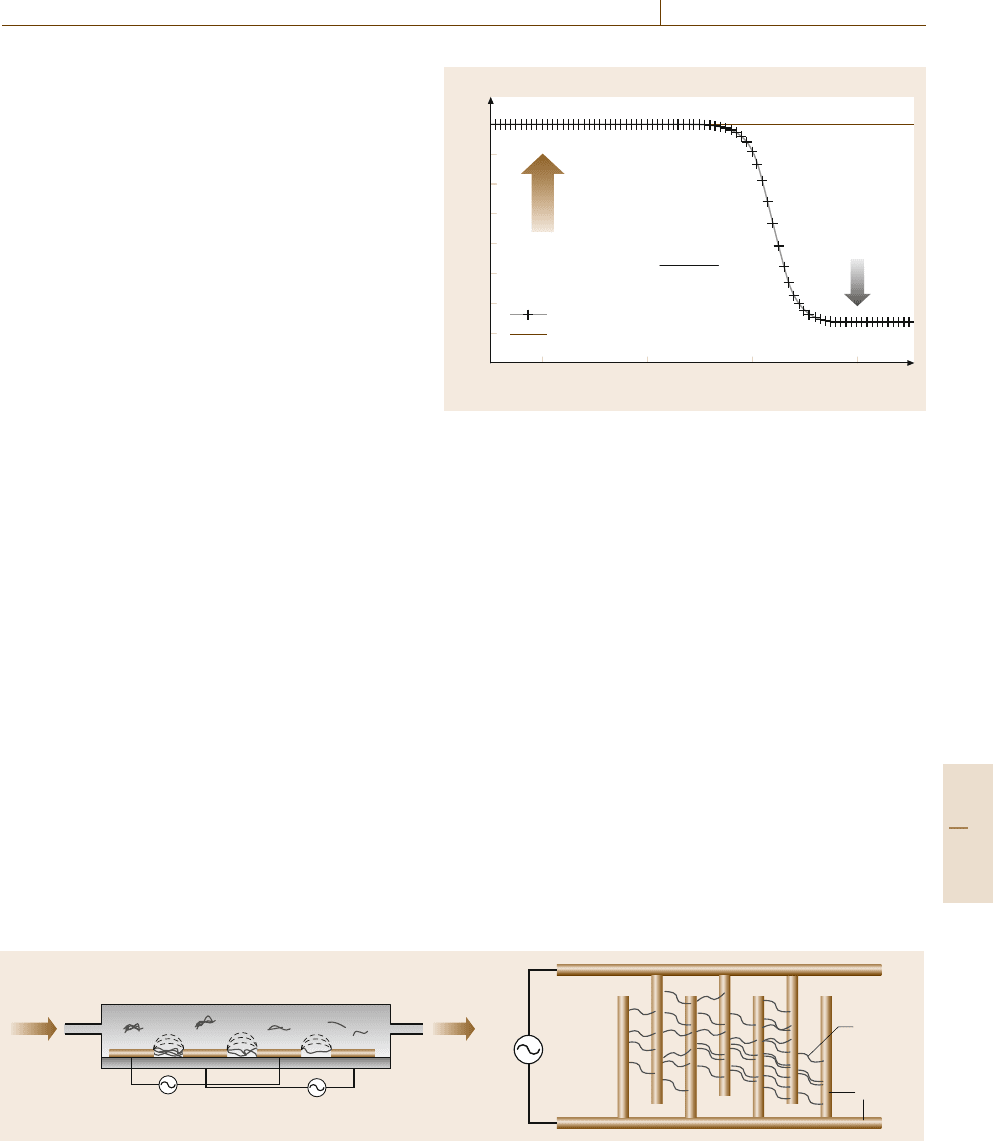
are obtained and shown in Fig. 53.17. The result in-
dicated that s-SWCNTs undergo a positive DEP force
at low frequencies (< 1MHz) while the DEP force
is negative when the applied frequency is larger than
10MHz. However, m-SWCNTs always undergo a pos-
itive DEP force at the applied frequency from 10 to
10
9
Hz. The result also matched the experimental re-
sult from [53.33], which showed that the positive DEP
effect on SWCNTs reduced as the frequency of ap-
plied electric field increased. In addition, the theoretical
result provides a better understanding of DEP manip-
ulation on different types of CNTs. DEP force can be
used to separate and identify different electronic types
of CNTs (metallic and semiconducting). Based on the
result shown in Fig.53.17, metallic CNTs can be se-
Apply AC voltage to
microelectrodes
CNT dilution
out (semiconducting
CNTs)
Micro-
electrodes
CNTs
CNT dilution in
(with metallic and
semiconducting CNTs)
a) b)
Semiconducting CNTs
Metallic
CNTs
Fig. 53.18a,b DEP microchamber to filter metallic CNT. Metallic CNTs are attracted on microelectrodes. Only semiconducting
CNTs flow to the outlet.
(a) Side view; (b) top view
10
2
10
4
10
6
Negative
DEP force
Positive
DEP force
10
8
K(ω)
K(ω) =
K(ω) =
Re [K(ω)] for s-SWCNT in alcohol
Re [K(ω)] for m-SWCNT in alcohol
ε
p
*
– ε
m
*
ε
p
*
+ 2ε
m
*
Frequency (Hz)
1
0.8
0.6
0.4
0.2
0
–0.2
–0.4
–0.6
Fig. 53.17 Plots of Re[K(ω)] that indicated positive and negative
DEP forces on different CNTs
lectively attracted to the microelectrodes by applying
AC voltage in the high frequency range (> 10MHz).
However, semiconducting CNTs cannot be attracted by
using the same frequency range; this makes the selec-
tion of semiconducting CNTs difficult. In order to select
semiconducting CNTs to make nanodevices, we fabri-
cated a microchamber (DEP chamber) with arrays of
microelectrodes to filter metallic CNTs in the medium.
Design and fabrication of the DEP chamber will be
discussed in the next section.
53.3.3 DEP Microchamber
for Separating CNTs
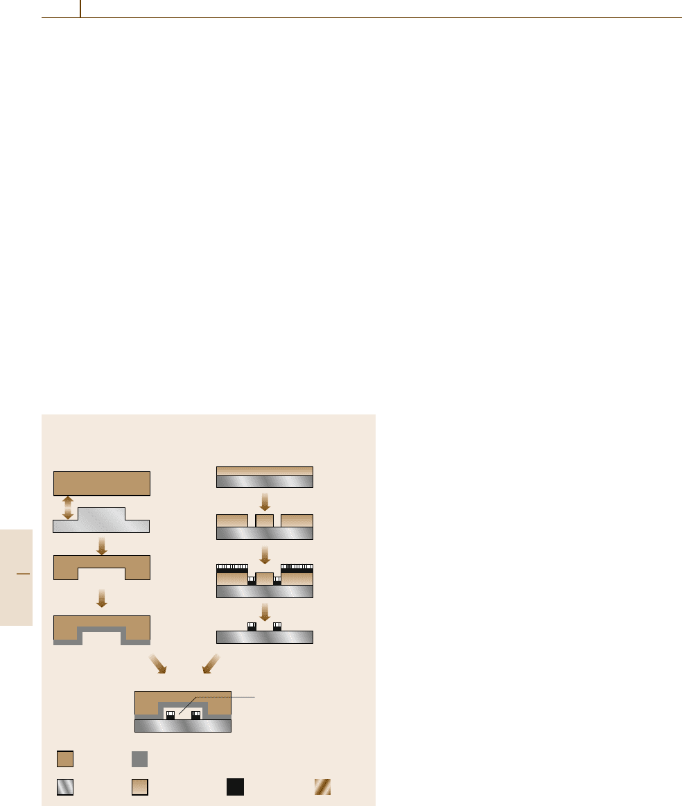
A DEP microchamber was designed and fabricated
to filter metallic CNTsinCNT suspension as shown
in Fig.53.18. Many finger-like gold microelectrodes
were first fabricated inside the chamber. The perfor-
mance of the filtering process was affected by the design
of these finger-like microelectrodes; the microelectrode
Part F 53.3
940 Part F Industrial Automation
structure with higher density induced a stronger DEP
force such that more CNTs could be attracted to the
microelectrodes. The gap distance between these mi-
croelectrodes is 5–10μm. The micropump pumped the
CNT suspension to the DEP chamber; a high frequency
AC voltage was applied to the finger-like microelec-
trodes so that metallic CNTs were attracted to them and
stayedintheDEP chamber. Semiconducting CNTs re-
mained in thesuspension and flowed out ofthe chamber.
Finally, the filtered suspension (with semiconducting
CNTs only) was transferred to an active nozzle for the
CNT deposition process. This will be described in the
next section.
The fabrication process of the DEP microcham-
ber is shown in Fig. 53.19. It was composed of two
different substrates. Polymethylmethacrylate (PMMA)
was used as the top substrate because it is electrically
and thermally insulating, optically transparent, and bio-
compatible. By using a hot embossing technique, the
PMMA substrate was patterned with a microchan-
nel (5mmL×1mmW×500 μm H) and a microcham-
ber (1cmL×5 mm W×500μm H) by replicating from
a fabricated metal mold. In order to protect the PMMA
Metal
mold
PMMA
Top substrate
Coat parylene C
UV glue bonding
Hot embossing of PMMA
substrate on metal mold
Bottom substrate
Spin on photoresist
on quartz substrate
Pattern and
develop PR
Deposit Ti and Au
Remove PR
Microchamber
PMMA Parylene C
Quartz Photoresist Titanium Gold
Fig. 53.19 The fabrication process of a DEP microchamber
substrate from the CNTs-alcoholsuspension, a parylene
C thin film layer was coated on the substrate, because
parylene resists chemical attack and is insoluble in all
organic solvents. Alternatively, quartz was used as the
bottom substrate,and arraysof the gold microelectrodes
were fabricated on the substrate by using a standard
photolithography process. A layer of AZ5214E pho-
toresist with thickness of 1.5μm was first spun onto
the 2
×1
quartz substrate. It was then patterned by
AB-M mask aligner and developed in an AZ300 de-
veloper. A layer of titanium with a thickness of 3nm
was deposited by thermal evaporator followed by de-
positing a layer of gold with thickness of 30nm. The
titanium provided a better adhesion between gold and
quartz. Afterwards, photoresist was removed in acetone
solution, and arrays of microelectrodes were formed on
the substrate. Finally, PMMA and quartz substrate were
bonded together by UV-glue to form a close cham-
ber. The fittings were connected at the ends of the
channel to form an inlet and an outlet for the DEP
chamber.
The separation performance of the DEP chamber
should be optimized for different nanoobjects. Several
parameters shouldbe considered in theprocess: thecon-
centration of nanoobjects in the suspension, the strength
of the DEP force, the flow rate of the suspension in
the DEP chamber, the structure of the channel, and the
microelectrodes of the DEP chamber.
53.3.4 Automated Robotic CNT Deposition
Workstation
In order to manipulate a specific type of CNTs precisely
and fabricate the CNT-based nanodevices effectively,
anewCNT deposition workstation has been devel-
oped as shown in Fig. 53.20. The system consists of
a microactive nozzle, a DEP microchamber, a DC mi-
crodiaphragm pump, and three micromanipulators. By
integrating these components into the deposition work-
station, a specific type of CNT can be deposited to
the desired position of the microelectrodes precisely
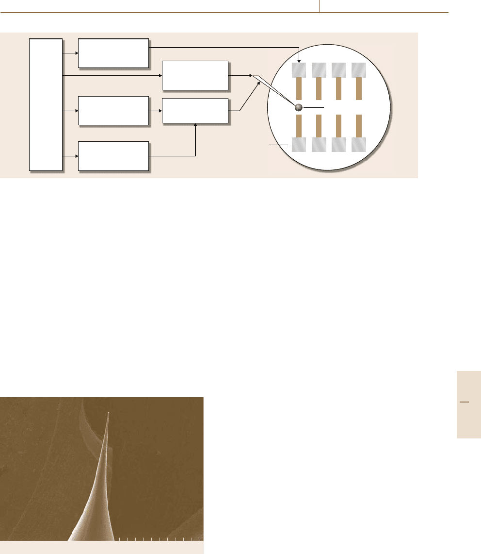
and automatically. The micron-sized active nozzle with
adiameterof10μm was fabricated from a micropipette
using a mechanical puller and is shown in Fig. 53.21.
It transferred the CNT suspension to the microelec-
trodes on a microchip, and a small droplet of the CNT
suspension (about 400 μm) was deposited on the mi-
crochip due to the small diameter of the active nozzle.
The volume of the droplet is critical because exces-
sive CNT suspension easily causes the formation of
multiple CNTs. The microactive nozzle was then con-
Part F 53.3
Nanomanufacturing Automation 53.3 Nanomanufacturing Processes 941
CNT suspension
PC
Electrical circuit of
AC voltage for
DEP manipulation
Another electrical
circuit of AC
voltage for filtering
Micropump for
delivering CNT
suspension
DEP chamber for
filtering
Micromanipulator
for positioning
active nozzle
Microelectrodes
on microchip
Active nozzle
Fig. 53.20 Illustration of the CNT deposition workstation
nected to the DEP chamber, which was designed to
filter metallic CNTs and select semiconducting CNTs
in the CNT suspension. The raw CNT suspension was
firstly pumped to the DEP chamber through a DC
microdiaphragm pump (NF10, KNF Neuberger, Inc.).
After the filtering process, the CNT suspension from
the DEP chamber was delivered to the active nozzle
for CNT deposition. By mounting the active nozzle
to one of the computer controllable micromanipulators
(CAP945, Signatone Corp.), the active nozzle could be
moved to the desired position of the microelectrodes
automatically. In order to apply the electric field to
the microelectrodes during the deposition process, the
other pair of micromanipulators was connected to an
electrical circuit and moved to the desired location of
the microelectrodes; therefore, AC voltage with dif-
ferent magnitudes and frequencies could be applied.
15 kV 12.3 mm ×50 SE(U) 9/4/2006 18:32 1 mm
Fig. 53.21 SEM image of the micro active nozzle with
10μm tip diameter
The micromanipulators, DC microdiaphragm pump,
and electrical circuit were connected to the computer
and controlled simultaneously during the deposition
process. By controlling the position of the micromanip-
ulators, the magnitude and frequency of the applied AC
voltage, and the flow rate of the micropump, the CNT
suspension can be handled automatically and deposited
to the desired position.
In the depositionprocess, AC voltage of 1.5V peak-
to-peak with frequency of 1kHz was applied; a positive
DEP force was induced to attract CNTstothemi-
croelectrodes. CNT deposition on multiple pairs of
microelectrodes was implemented by controlling the
movement of the micromanipulator, which was con-
nected with the active nozzle. Since the position of
each pair of the microelectrodes was known from the
design CAD file, distances (along x and y axes) be-
tween each pair of microelectrodes were then calculated
and recorded in the deposition system. At the start, the
active nozzle was aligned to the first pair of the micro-
electrodes as shown in Fig. 53.22a. The position of the
active nozzle tip was 2mm above the microchip. When
the deposition process started, the active nozzle moved
down 2mm and a droplet of CNT suspension was de-
posited on the first pair of microelectrodes as shown
in Fig.53.22b. Afterwards, the active nozzle moved up
2mm and traveled to the next pair of microelectrodes
as shown in Fig. 53.22c. The micromanipulator moved
down again to deposit the CNT suspension on the sec-
ond pair of microelectrodes as shown in Fig.53.22d.
This process repeated continuously until CNT suspen-
sion was deposited on each pair of microelectrodes on
the microchip. By activating the AC voltage simultane-
ously, a CNT was attracted and connected between each
pair of microelectrodes. The activation time was short
Part F 53.3
942 Part F Industrial Automation
Active nozzle
2nd
Electrodes
2nd
Electrodes
3rd
Electrodes
2nd
Electrodes
CNT suspension
1st
Electrodes
a) b) c) d)
Fig. 53.22a–d CNT deposition process flow observed under the optical microscope. (a) The active nozzle tip aligned
to the initial electrodes,
(b) CNT suspension deposited, (c) the nozzle was moving to next electrodes, and (d) CNT
suspension deposited on the second electrodes
(≈ 2s) to avoid the formation of bundled CNTsonthe
microelectrodes.
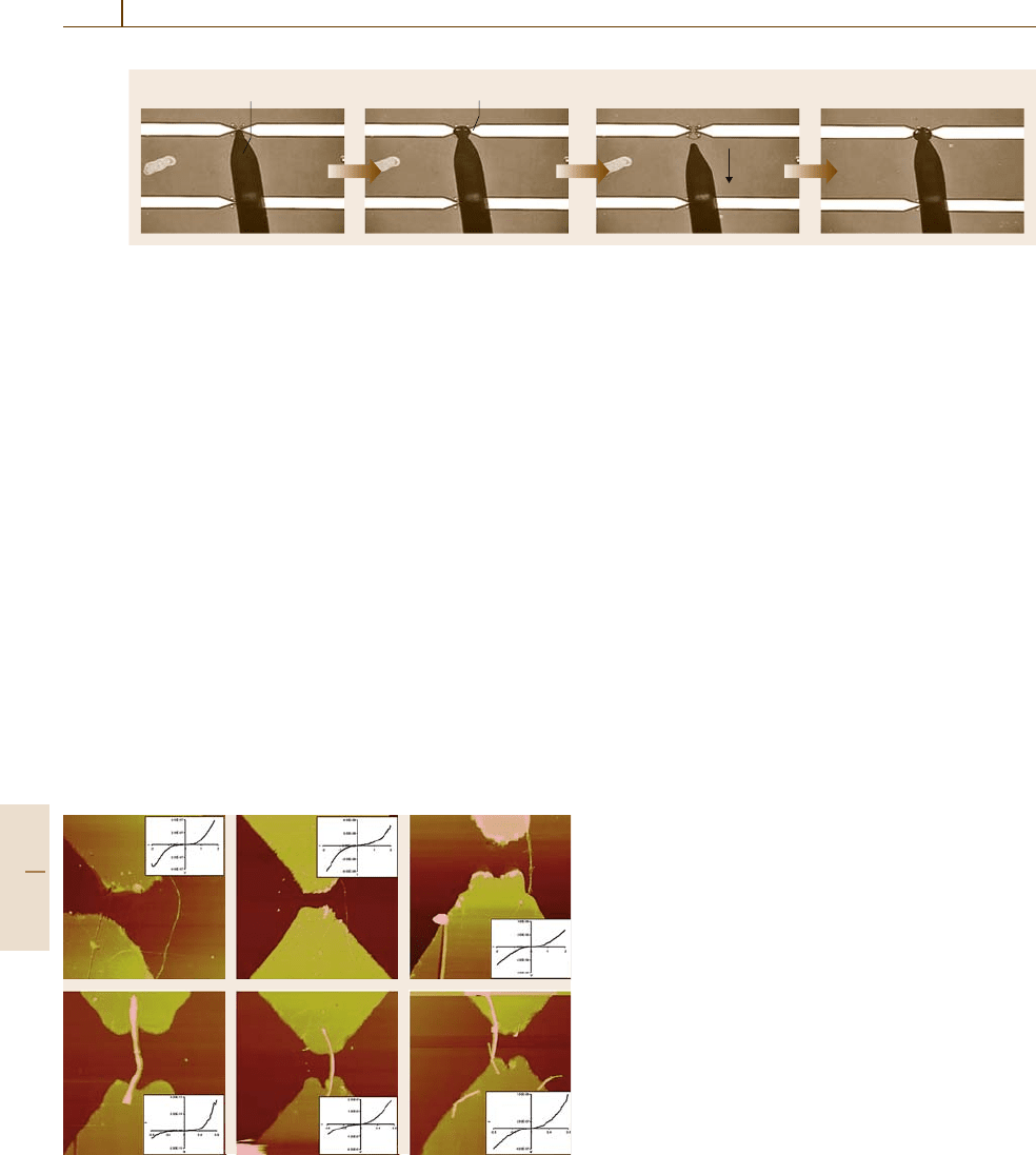
After the deposition process, AFM was used to
check theCNT formation as shown inFig.53.23.Some-
times, there are some impurities or more than one
CNT trapped between the microelectrodes as shown
in Fig.53.23f. Therefore, it is necessary to take another
step to clean up the microelectrodes gap area and adjust
the position of the CNT to make the connection. This fi-
nal step is very critical and is termed CNT assembly; it
can be done by our AFM-based nanomanipulation sys-
tem. I–V characteristicsof theCNT-based devices were
also obtained as shown inthe inset images of Fig.53.23.
Based on the results, this indicates that both SWCNTs
and MWCNTs could be repeatedly and automatically
manipulated between the microelectrodes by using the
deposition system. This CNT deposition workstation
integrates all essential components to manipulate the
specific type of CNTs to desired positions precisely
a) b) c)
d) e) f)
Fig. 53.23a–f AFM images showing the individual CNTswas
deposited on the microelectrodes.
Panels (a–c) are SWCNTs,
panels (d–f) are MWCNTs.The inset images are the corresponding
I–V curves of each CNT
by DEP force. The development of this system pro-
duces benefits to the assembling and manufacturing of
CNT-based devices. The yield of depositing CNTson
the microelectrodes is very high after optimizing the
following factors: the concentration of the CNT suspen-
sion, the volume of theCNT suspension droplet, and the
activation time, magnitude and frequency of the applied
electric field.
In order to validate the separation performance of
different CNTsbytheDEP chamber, experiments for
both raw CNT suspension (before passing through the
DEP chamber) and filtered CNT suspension were con-
ducted, respectively. The procedure for preparing the
CNT suspension was the same as the process presented
in the previous section. SWCNT powder (BU-203,
Bucky USA, Nanotex Corp.) was dispersed in an al-
cohol liquid medium, and the CNT suspension was
put in the ultrasonicator for 15 min. The length of the
SWCNT is 0.5–4μm. Finally, the raw SWCNT sus-
pension was prepared and the concentration was about
1.1μg/ml. Afterwards, the separation process was per-
formed on the raw SWCNT suspension as illustrated
in Fig.53.24. During the process, the raw SWCNT
suspension was pumped to the DEP chamber through
the micropump. The flow rate was about 0.03l/min.
A high frequency AC voltage (1.5Vpp, 40MHz) was
applied to the microelectrodes in the DEP chamber; it
induced a positive DEP force on metallic SWCNTsin
the suspension but a negative DEP force on semicon-
ducting SWCNTs. Since the metallic SWCNTs were
attracted to the microelectrodes and stayed in the DEP
chamber, it was predicted that only semiconducting
SWCNTs remained in the filtered SWCNT suspension.
The filtered SWCNT suspension was then collected at
the outlet of the chamber for later CNT disposition
process.
After preparing the raw and filtered SWCNT
sus-
pension, the deposition process was performed by using
our CNT deposition workstation, which was intro-
Part F 53.3
Nanomanufacturing Automation 53.3 Nanomanufacturing Processes 943
Micropump
Raw CNT
suspension
Filtered CNT
suspension
Selection chamber
Fig. 53.24 The CNT filtering process
duced in the previous section. In the experiment, the
raw SWCNT suspension and the filtered SWCNT sus-
pension were deposited on the microchip 20 times,
respectively. The electronic properties of CNTs in both
suspensions were then studied by measuring the I–V
curves. The yields to obtainsemiconducting CNTs from
the raw CNT suspension and filtered CNT suspension
were also compared. Based on the preliminary results,
the yield of depositing semiconducting SWCNTs (from
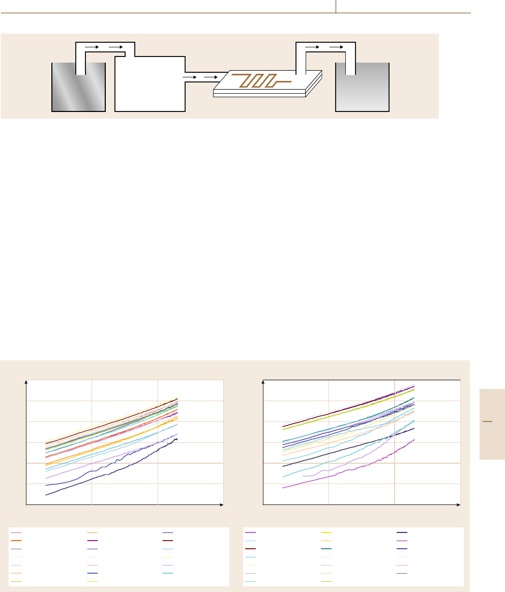
the raw SWCNT suspension) was about 33% as shown
in Fig.53.25; the yield of depositing semiconducting
SWCNTs (from the filtered SWCNT suspension) was
about 65% as shown in Fig.53.25. The yield to form
semiconducting CNTs is very important because many
devices require materials with semiconducting prop-
erties. The results indicated that there was significant
improvement in forming semiconducting CNTsonthe
microelectrodes by using our DEP chamber. The yield
0.01 0.1 1 10
Log voltage (V)
10
–3
10
–4
10
–5
10
–6
10
–7
10
–8
10
–9
1– Metallic
4– Metallic
7– Semiconducting
10– Metallic
13– Semiconducting
16– Metallic
19– Metallic
2– Semiconducting
5– Metallic
8– Semiconducting
11– Metallic
14– Semiconducting
17– Metallic
20– Semiconducting
3– Semiconducting
6– Metallic
9– Metallic
12– Metallic
15– Metallic
18– Metallic
a) Log current (A)
0.01 0.1 1 10
Log voltage (V)
10
–4
10
–5
10
–6
10
–7
10
–8
10
–9
10
–10
10
–11
1– Semiconducting
4– Semiconducting
7– Metallic
10– Metallic
13– Semiconducting
16– Semiconducting
19– Semiconducting
2– Metallic
5– Semiconducting
8– Semiconducting
11– Semiconducting
14– Semiconducting
17– Semiconducting
20– Metallic
3– Metallic
6– Metallic
9– Semiconducting
12– Semiconducting
15– Semiconducting
18– Metallic
b) Log current (A)
Fig. 53.25a,b I–V characteristics of SWCNTs. (a) For the raw SWCNT suspension, (b) for the filtered SWCNT suspension
in forming semiconducting CNTs changed from 33%
(before the filtering process) to 65% (after the filtering
process). The yield should be improved by optimizing
the concentration of CNT suspension, the strength of
the DEP force, the flow rate of the suspension in the
DEP chamber, the structure of the channel, and the mi-
croelectrodes of the DEP chamber.
The yield to form semiconducting CNTs is very im-
portant because it affects the successful rate to fabricate
nanodevices. The yield to form semiconducting CNTs
was increased by using our system. Although there is
a synthesis that produces nearly90% of semiconducting
CNTsbyPECVD [53.49], both CNT synthesis methods
and post-processing separation methods are important
and can be combined for differentapplications. Oursep-
aration system is a post-processing method, which can
be used together with different CNT synthesis methods.
Since our system used electrical signal to control the
Part F 53.3
944 Part F Industrial Automation
0 5 10 15
IR laser is ON
IR laser is OFF
20 25 30
Current (nA)
Time (s)
0
–0.2
–0.4
–0.6
–0.8
–1
–1.2
–1.4
–1.6
–1.8
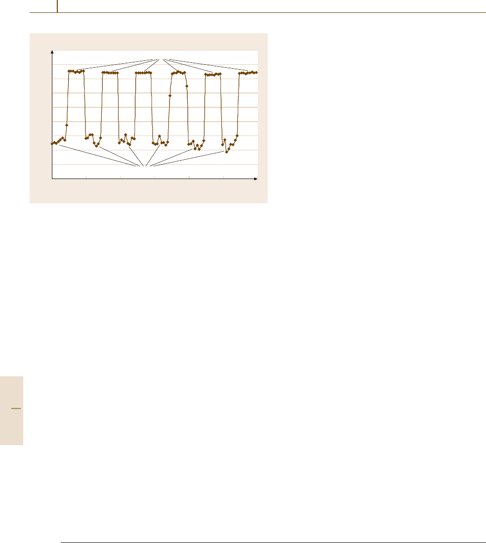
Fig. 53.26 Temporal photoresponses of a CNT-based IR detector
DEP manipulation and separation, it can be integrated
with current robotic manufacturing systems easily, and
eventually the process can be operated automatically
and precisely. As a result, batch nanomanufacturing of
nanodevices can be achieved by this system.
53.3.5 CNT-Based Infrared Detector
When semiconducting CNTs are deposited on the mi-
croelectrodes, the photonic effects of the CNT-based
nanodevice can be studied. For example, a CNT device
was put under the infrared (IR) laser source (UH5-
30G-830-PV, World Star Tech, optical power: 30mW;
wavelength: 830 nm), and the photocurrent from the
CNT-based nanodevice was measured. The laser source
was configured to switch on and off in several cycles;
the temporal photoresponses of the device are shown
in Fig.53.26. The experimental result showed the CNT-
based device was sensitive to the IR laser, so CNTs can
be used to make novel IR detectors. More detail design
and fabrication of CNT-based IR detectors are given
in [53.50–52]
53.4 Conclusions
Automated nanomanipulation is desirable to increase
the efficiency and accuracy of nanoassembly. Auto-
mated nanoassembly of nanostructures isvery challeng-
ing because of the manipulation path generation for
different nanoobjects, position errors due to random
drift, and cantilever deformation during nanomanip-
ulation. This chapter discussed automated nanoma-
nipulation technology for nanoassembly. Automated
nanomanipulation methods of nanoobjects were devel-
oped, and an automated local scanning method was
presented to compensate for the random drift. A CAD
guided automated nanoassembly method was devel-
oped. CAD guided automated nanoassembly was able
to open a door to assembly of complex nanostructures
and nanodevices. The effectiveness of the system has
also been verified by inscribing nano features on soft
surface, manipulating nanoparticles DNA molecules
and characterization of biological samples [53.53–56].
Moreover, CNT separation by a DEP chamber and the
development of an automated CNT deposition work-
station that applies DEP manipulation on CNTs were
presented. The system assembles semiconductingCNTs
to the microelectrodes effectively and, therefore, it is
possible to improve the success rate to fabricate nano-
devices. The separation method developed in this paper
is a post-processing method, which can be used together
with different CNT synthesis methods. Since our sys-
tem used electrical signals to control CNT separation
and DEP manipulation, it can be integrated into current
robotic manufacturing systems easily, and eventually it
will be possibleto operatethe process automatically and
precisely. It opens the possibility of batch fabricating
CNT-based devices. Furthermore, the nanomanufac-
turing process is not limited to CNTs, but it can be
used on other nano materials such as ZnO and InSb
nanowires etc. The development of the nanomanufac-
turing process will achieve different novel nano devices
effectively.
References
53.1 G. Binning, C.F. Quate, C. Gerber: Atomic force
microscope, Phys. Rev. Lett. 56(9), 930–933 (1986)
53.2 D. Wang, L. Tsau, K.L. Wang, P. Chow: Nanofabri-
cation of thin chromium film deposited on Si(100)
Part F 53
