Hoffman D.M., Singh B., Thomas J.H. (Eds). Handbook of Vacuum Science and Technology
Подождите немного. Документ загружается.

664
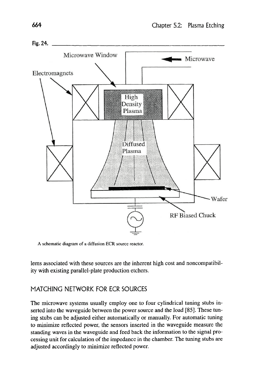
Fig.
24.
Chapter 5.2: Plasma Etching
Microwave Window
Electromagnets
Microwave
Wafer
RF Biased Chuck
A schematic diagram of a diffusion ECR source reactor.
lems associated with these sources are the inherent high cost and noncompatibil-
ity with existing parallel-plate production etchers.
MATCHING NETWORK FOR ECR SOURCES
The microwave systems usually employ one to four cylindrical tuning stubs in-
serted into the waveguide between the power source and the load [85]. These tun-
ing stubs can be adjusted either automatically or manually. For automatic tuning
to minimize reflected power, the sensors inserted in the waveguide measure the
standing waves in the waveguide and feed back the information to the signal pro-
cessing unit for calculation of the impedance in the chamber. The tuning stubs are
adjusted accordingly to minimize reflected power.
5.2.7 New Trends
665
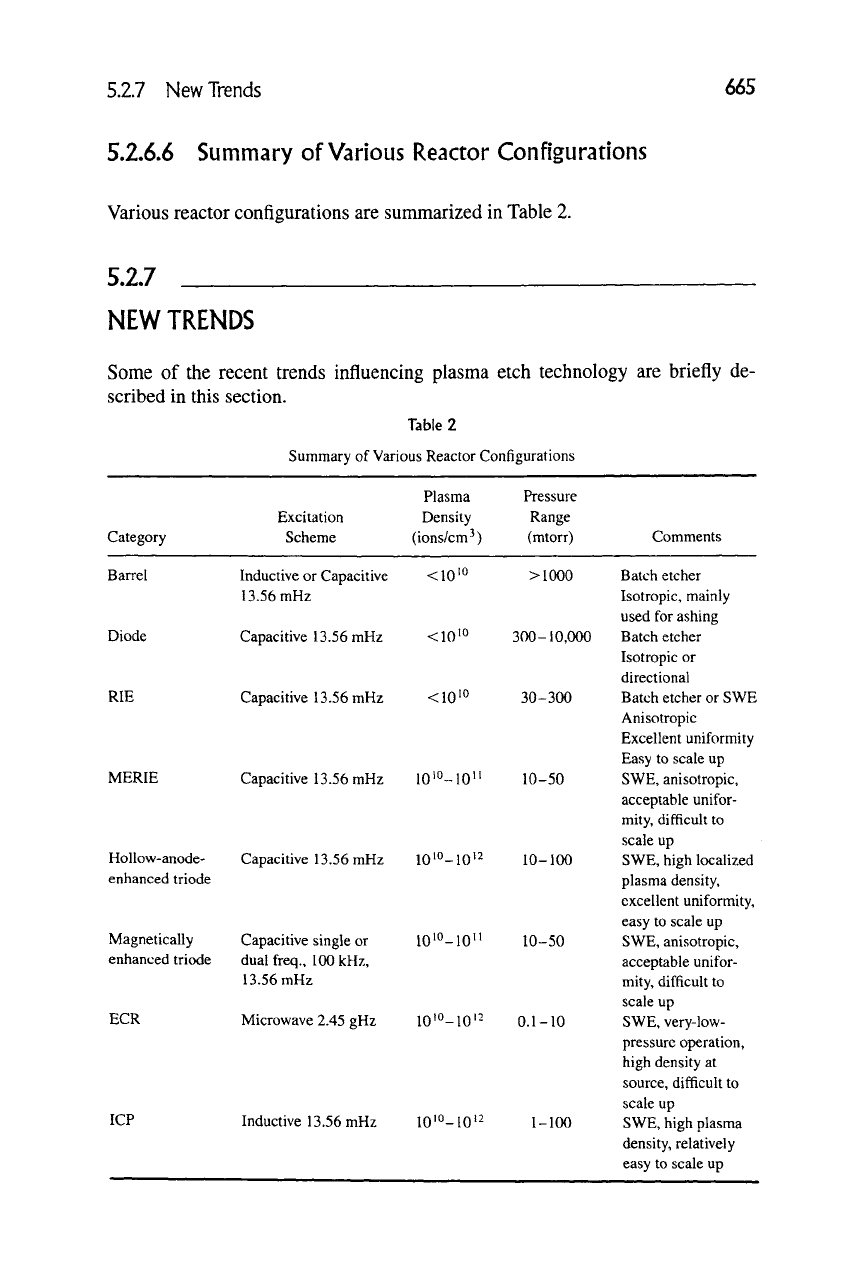
5.2.6.6 Summary of Various Reactor Configurations
Various reactor configurations are summarized
in
Table
2.
5.2.7
NEW TRENDS
Some
of the
recent trends influencing plasma etch technology
are
briefly
de-
scribed
in
this section.
Table
2
Summary
of
Various Reactor Configurations
Category
Barrel
Diode
RIE
MERIE
Hollow-anode-
enhanced triode
Magnetically
enhanced triode
ECR
ICP
Excitation
Scheme
Inductive or Capacitive
13.56 mHz
Capacitive 13.56 mHz
Capacitive 13.56 mHz
Capacitive 13.56 mHz
Capacitive 13.56 mHz
Capacitive single or
dual freq., 100 kHz,
13.56 mHz
Microwave 2.45
gHz
Inductive 13.56 mHz
Plasma
Density
(ions/cm^)
<10'o
<10'o
<10'o
lO'O-lO"
10»0-10'2
lO'O-lO"
10'0-10'2
10'°-10'2
Pressure
Range
(mtorr)
>1000
300-10,000
30-300
10-50
10-100
10-50
0.1-10
1-100
Comments
Batch etcher
Isotropic, mainly
used for ashing
Batch etcher
Isotropic
or
directional
Batch etcher or SWE
Anisotropic
Excellent uniformity
Easy
to
scale up
SWE,
anisotropic,
acceptable unifor-
mity, difficult
to
scale up
SWE,
high localized
plasma density,
excellent uniformity,
easy to scale up
SWE,
anisotropic.
acceptable unifor-
mity, difficult
to
scale up
SWE,
very-low-
pressure operation,
high density
at
source, difficult
to
scale up
SWE,
high plasma
density, relatively
easy
to
scale up
666 Chapter 5.2: Plasma Etching
END POINT DETECTION
End point detection of
a
given etch process has become very critical because very
thin layers (<100 A) used for modern VLSI and ULSI circuits cannot tolerate
overetching. Laser reflection interferometry [86] was used in early days for end
point detection. At present, optical emission spectroscopy (OES) technique is be-
ing widely used in production for end point control. In OES, the end point is de-
termined by following time dependence of a selected wavelength of the optical
spectmm emitted by the plasma representing either a reactant or a by-product. By
monitoring the change in optical signal associated with completion of an etch re-
action, the end point can be called and the etch process can be terminated.
Presently available OES end point detection equipment are reaching a limit for
the etch applications involving etching of very little exposed areas (<2%) on the
wafer (such as via etch), due to very low signal-to-noise ratio. A major emphasis
is being given to optimization of the detection capability of the OES equipment
[87,88].
In parallel, several other techniques such as ellipsometry [89], plasma
impedance monitoring [90], infrared absorption spectroscopy [91], and neural
networks [92] are also being investigated.
CLUSTER TOOLS
In the past few years, many etch chambers have been integrated on the same plat-
form in a form of a cluster tool. The concept of a cluster tool was developed to
improve yield by reducing particles through automated, in-vacuum transfer be-
tween etch modules. The throughput is also increased because many operations
can be done in parallel. Clustering, however, places stringent requirements on
equipment reliability due to interdependence of the equipment set and the inher-
ent lack of flexibility [93,94].
ELECTROSTATIC CHUCKS
Electrostaic chucks are being integrated on proven etch platforms by almost all
equipment vendors as a replacement for conventional Helium backside or cryo-
genically cooled clamped electrodes [95]. The electrostatic chuck holds the wafer
with no front side contact, offering significant improvement in total number of
dies that can be processed. In addition, the elimination of moving clamp parts help
reduce particle generation and simplifies chamber design.
ORIGINAL EQUIPMENT MANUFACTURE [OEM] SUPPORT
In past few years, the up-time and reliability of equipment has become very criti-
cal,
because of financial constraints in high-volume manufacturing of semicon-
References 667
ductor circuits. The software and robotic systems used on an etch tool are con-
stantly being upgraded. Also, in many cases the etch equipment is linked to the
OEM through a telephone line so that the performance of the machine can be
monitored on-line and potential problems can be diagnosed and resolved without
sending out a field service engineer.
GUARANTEED PROCESSES
In the initial days of the semiconductor industry, the majority of the etch
processes were developed by engineers in the fabrication facility, on an in-house-
built or a vendor-supplied reactor. In the past few years, the trend has been shifted
toward process development by the OEM. At present, the majority of the produc-
tion machines are being sold with a guaranteed process performance for a specific
application.
REFERENCES
1.
A. T. Hell, Spatial distribution of electron density and electric field strength in a high-frequency
discharge, Ind. Chem. Eng. Fimdam., 9 (1970) 160-166.
2.
M. J. Kushner, Mechanisms for power deposition in Ar/SiH4 capacitively coupled RF dis-
charges, IEEE
Trans,
on Plasma Sci, PS-14 (1986) 188-196.
3.
D. Flamm and G. Herb, Plasma Etching: An Introduction, edited by D. Mannos and D. Flamm
(Academic Press, San Diego, 1989), chap. 1, p. 37.
4.
H. S. Butler and G. S. Kino, Plasma sheath formation by radio-frequency fields, Phys. Fluids, 6
(1963) 1346-1355.
5.
K. Riemann, Theoretical analysis of the electrode sheath in RF discharges, 7. Appl. Phys., 65
(1989)999-1004.
6. M. A. Liberman, Dynamics of a coUisional, capacitive RF sheath, IEEE
Trans,
on Plasma Sci.,
PS-17 (1989)
338-341.
7.
D. Vender and R. Boswell, Electron-sheath interaction in capacitive radio-frequency plasmas,
J.
Vac.
Sci. TechnoL, A10(4) (1992) 1331-1338.
8. P. M. Vallinga, P. M. Meijer, and F. J. de Hoog, Sheath properties of RF plasmas in a parallel
plate etch reactor; the high frequency regime, J. Phys. D. Appl. Phys., 22 (1989) 1650-1657.
9. G. R. Misium, A. J. Lichtenberg, and M. Liberman, Macroscopic modeling of radio frequency
plasma discharges, J.
Vac.
Sci. TechnoL, A7(3) (1989) 1007-1013.
10.
D. E. Bohm, Minimum ionic kinetic energy for a stable sheath, in The Characteristics of Elec-
trical Discharges in Magnetic Fields, edited by A. Guthrie and R. K. Walkerling (McGraw-Hill,
New York, 1949).
11.
F. F. Chen, Introduction to Plasma Physics and Controlled Fusion, vol. 1, 2nd ed. (Plenum
Press,
New York, 1984).
12.
J. Meichsner, H. U. Poll, and K. H. Wixkleder, Negative ions in a glow discharge of tetrafluoro-
methane, Contrib. Plasma Phys., 25(5) (1985) 503-512.
13.
N. St. J. Braithwaite and J. E. Allen, Boundaries and probes in electronegative plasmas, J. Phys.
D:
Appl. Phys., 21 (1988) 1733-1737.
668 Chapter 5.2: Plasma Etching
14.
R. Gottscho, Glow-discharge sheath electric fields: Negative-ion, power, and frequency effects,
Phys. Review, A36(5) (1987) 2233-2240.
15.
Laura Peters, Plasma etch chemistry: The untold story. Semiconductor International (May 1992)
66-71.
16.
J. W. Coburn and H. F. Winters, Ion and electron assisted gas surface chemistry—An important
effect in plasma processing, / Appl. Phys., 50 (1979) 3189-3194.
17.
E. Kay, J. Coburn, and A. Dilks, Plasma chemistry of fluorocarbons as related to plasma etching
and plasma polymerization. Topics Current Chem., 94 (1980)
1
-9.
18.
J. Cook and K. Donohoe, Etching issues at 0.35 pm and below. Solid State Technology (April
1991)119-124.
19.
R. d'Agostino, F. Cramarossa, S. DeBenedictis, and G. Ferraro, Spectroscopic diagnosis of
CF4-O2 plasmas during Si and Si02 etching processes, / Appl. Phys., 52 (1981) 1259-1265.
20.
L. Ephrath, Dry-etching for VLSI—A review, / Electrochem. Soc, 129 (1982) 2282-2287.
21.
D. Economou, E. Aydil, and G. Barna, In situ monitoring of etching uniformity in plasma reac-
tors.
Solid State Technol, 34(4) (1991) 107
-111.
22.
P. Singer, Plasma etch: A matter of fine-tuning, Semiconductor International, 12 (1995) 65-68.
23.
Y. Liu and M. Flowers, Kinetics of triode mode reactive ion etching of Si (100) wafers by chlo-
rine plasmas: Temperature and DC self-bias effects.
Vacuum
42(18) (1991) 1213-1217.
24.
A. Watts and W. Varhue, Low temperature etching of silicon trenches with SFg in an electron
cyclotron resonance reactor, J.
Vac.
Sci Technol, A10(4) (1992) 1313-1330.
25.
A. De Dios, E. Castan, L. Bailon, J. Barbolla, M. Lozano, and E. Lora-Tamayo, RIE-induced
damage in MOS structures, Solid-State Electronics, 33(11) (1990) 1419-1423.
26.
D. Misra, W. Zhong, R. Bartynski, V. Patel, and B. Singh, Etch induced damage in high density
inductively coupled plasma etching reactors, Semicond. Sci. Technol., 11 (1996)
816-821.
27.
X. Li, T. Brozek, F. Preuninger, D. Chan, and C. Viswanathan, Evaluation of Plasma Damage
Using Fully Processed MOS Transistors, J.
Vac.
Sci. Technol., Bll(l) (1996) 571-576.
28.
V. Menon, Fine Particle Society Annual Meeting, Santa Carla, CA (July 1991).
29.
S. J. Choi and M. J. Kushner, The role of negative ions in the formation of particles in low pres-
sure plasmas. Appl. Phys. Letters, 62 (1993) 2562-2564.
30.
G. Selwyn, A phenomenological study of particulates in plasma tools and processes, Jpn. J.
Appl. Phys., 32(6B) (1993) 3068-3073.
31.
J. Maa, H. Gossenberger, and R.
Paff,
Effect of post-etch treatment on chlorine concentration of
AISi and Ti capped AlSi films, J.
Vac.
Sci. Technol., B8(5) (1990) 1052-1057.
32.
N. Parekh and J. Price, VLSI Multilevel Interconnection Conference Proceedings, Phoenix, AZ
(IEEE, New York, 1989), pp.
506-511.
33.
S. Pearson, M. Wilders, and A. Chambers, Reactive ion etching of AlSiCu alloy films. Semicon-
ductor International (February 1987), pp. 97-100.
34.
T. Y. Fok, Electrochemical Society Extended Abstracts 80-1, 1980 (Electrochemical Society,
Pennington, NJ, 1980), Abstract No. 115.
35.
H. Busta, R. E. Lajos, and D. Kiewit, Plasma etch monitoring with laser interferometry, Solid
State Technol., 22(2) (1979) 62-65.
36.
V Godyak and R. Piejak, In situ simultaneous radio frequency discharge power measurements,
./.
Vac.
Sci. Technol., A8(5) (1990) 3833-3837.
37.
B. Andries, G. Ravel, and L. Peccoud, Electrical characterization of radio frequency parallel
plate capacitively coupled discharges, J.
Vac.
Sci. Technol., A7(4) (1989) 2774-2783.
38.
G. Selwyn and E. Key, Spatially resolved optical emission studies of fluorocarbon RF plasma
through the use of UV-transmitting optical fibers, Plasma Chemistry and Plasma Processing,
5(2) (1985) 183-199.
39.
T. Chau and K. Kao, Optical emission spectra of microwave oxygen plasmas and fabrication of
SiO.
films. J.
Vac.
Sci. TechnoL B14(l) (1996) 527-532.
References 669
40.
K. Maruyama, K. Ohkouchi, Y. Ohtsu, and T. Goto, CF3, CF2 and CF radical measurements in
RF CHEF3 etching plasma using infrared diode laser absorption spectroscopy, Jpn. J. Appl.
Pliys., 33(7B) (1994) 4298-4302.
41.
H. C. Sun, E. Whittaker, Y. Bae, C. Ng, V. Patel, W. Tam, S. McGuire, B. Singh, and B. Gallois,
Combined wavelength and frequency modulation spectroscopy: A novel diagnostic toll for ma-
terials processing. Applied Optics, 32(6) (1993) 885-893.
42.
J. Coburn, A system for determining the mass and energy of particles incident on a substrate in
a planar diode sputtering system. Rev. Sci. lustrum., 41(8) (1970) 1219-1223.
43.
D. W. Grave, T. J. Knight, X. Cheng, B. Krogh, M. Gibson, and J. LaBrosse, Process control
based on quadrupole mass spectroscopy, J.
Vac.
Sci. TeclmoL, B14(l) (1996) 489-493.
44.
H. Hermansdorfer, Microwave diagnostic techniques, in Plasma Diagnostics, edited by
W. Lochte-Holtgreven (North-Holland, Amsterdam, 1968).
45.
I. Langmuir and H. Mott-Smith, Collected works of Irving Langmuir, Vol. 4 (Pergamon Press,
Long Island City, NY (1961), pp. 99-132.
46.
P Chung, L. Talbot, and K. Touryan, Electrical probes in stationary and flowing plasma: Part 1,
Collisional and transitional probes; Part 2, Continuum probes, AIAA Journal, 12(2) (1974)
133-154.
47.
B. E. Cherrington, The use of electrostatic probes for plasma diagnostis —A review, Plasma
Chemistry and Plasma Processing, 2(2) (1982) 113-140 and references therein.
48.
A. R. Reinberg, Plasma processing with a planar reactor. Circuits Mfg. (April 1979)
25-31.
49.
G. K. Herb, D. Rigger, and K. Shields, Silicon trench etch in a hex reactor. Solid State Technol-
ogy (October 1987) 109-115.
50.
V. Donnelly and D. Flamm, Effects of frequency on optical emission, electrical ion, and etching
characteristics of a radio frequency chlorine plasma, J. Appl. Phys., 58(6) (1985) 2135-2144.
51.
S. Schultheis, Single-wafer high rate RIE employing magnetron discharge. Solid State TeclmoL,
28(4) (1985) 233-237.
52.
R. Hill, Characterization of a low pressure, high ion density, plasma metal etcher, J. Vac. Sci.
Technol., B14(l) (1996)
547-551.
53.
D. Sheehan and N. Rynn, Negative ion plasma sources. Rev. Sci. Instrum., 59(8) (1988) 1369-
1375.
54.
B. Singh and P. R. Denton, The magnetron: Many gains and more to come. Optical Spectra,
15(10) (1981)
77-81.
55.
J. W. Coburn, Plasma Etching and Reactive Ion Etching (American Vacuum Society, New York,
1982),
and references therein.
56.
C. M. Melliar-Smith and C. J. Mogab, in Thin Film Processes, ed. by J. L. Vossen and W. Kern
(Academic Press, New York, 1979).
57.
R. Kraft, T. Boonstra, and S. Prengle, Etching 0.35 pun polysilicon gates on a high density heli-
con etcher, J.
Vac.
Sci. Technol, B145(l) (1996) 543-546.
58.
R. Waits, Planar magnetron sputtering, y.
Vac.
Sci. Technol., 15(2)
{\91S)
179-187.
59.
J. Thornton, Magnetron sputtering: Basic physics and application to cylindrical magnetrons,
J.
Vac.
Sci. Technol., 15(2) (1978) 171-177.
60.
J. Vossen and
W.
Kern, eds.. Thin Film Processes (Academic Press, New York, 1978).
61.
H. Kinoshita, T. Ishida, and S. Ohno, Highly uniform magnetron etching system using an annu-
lar permanent magnet, Appl. Phys. Lett. 50(25) (1987) 1838-1841.
62.
H. Okano, T. Yamazaki, and Y. Horiike, High rate reactive ion etching using a magnetron dis-
charge. Solid State Technol, 25(4) (1982) 166-170.
63.
A.
Hoff,
T. Esry, and K. Nauka, Monitoring plasma damage: A real-time, noncontact approach.
Solid State Technol, 39(4) (1996) 139-148.
64.
W. En, B. Linder, and N. Cheung, Modeling of oxide charging effects in plasma processing,
J.
Vac.
Sci Technol, B14(l) (1996) 552-556.
670 Chapter 5.2: Plasma Etching
65.
G. J. Gorin, U.S. Patent No. 4,464,223 (August 1984).
66.
J. H. Thomas III and B. Singh, Effect of the radio-frequency voltage phase in a balanced triode
plasma etching reactor, /
Vac.
Sci.
Techno!.,
A10(5) (1992) 3070-3075.
67.
V. Patel, Characterization of Advanced
Etching
Reactors
Using
Novel Diagnostic
Tools,
unpub-
lished doctoral thesis. New Jersey Institute of Technology, 1993.
68.
E. Bogle-Rohwer, D. Gates, L. Hayler, H. Kurasaki, and B. Richardson, Wall profile control in a
triode etcher. Solid
State
Technoi, 28 (1985)
251
-255.
69.
J. F. Donohue, M. Kent, and A. Sampson, Geometric focusing technology applied to Si02 etch-
ing,
J.
Vac.
Sci.
TechnoL,
B14(l) (1996) 466-470.
70.
J. Andrews and
J.
Allen, Theory of
a
double-sheath between two plasmas, Proc.
Roy.
Soc. Lon.,
A320 (1971) 459-472.
71.
B. Singh, unpublished doctoral thesis, Investigation of
Some
of
the
Physical Processes Occur-
ring in High Current
Ion
Sources, University of Aston, Birmingham, UK, 1978.
72.
P. Laporte, Y. Melaku, and M. Goethals, Magnetically confined dry etching for silylated resist
development. Solid State Technol, 34(4) (1991) 69-73.
73.
H. Kinoshita and O. Matsumolo, A new supermagnetron plasma etcher remarkably suited for
high performance etching,
J.
Vac.
Sci. Technol, B9(2) (1991) 325-333.
74.
B. Singh, J. H. Thomas, III, and V. Patel, Magnetic multipole based reactive ion etching reactor,
Appl.
Phys.
Lett.,
60(19) (1992) 2335-2337.
75.
J. Hopwood, Review of inductively coupled plasmas for plasma processing. Plasma Sources Sci.
Technol, 1(2) (1992) 109-116.
76.
J. Givens, S. Geissler, J. Lee, O. Cain, J. Marks, P. Keswick, and C. Cunningham, Selective dry
etching in a high density plasma for 0.5 /xm CMOS technology, J.
Vac.
Sci. Technol, B12(l)
(1994)427-432.
77.
R. B. Piejak, V. Godyak, and B. Alexandrovich, A simple analysis of
an
inductive RF discharge.
Plasma Sources Sci Technol, 1(2) (1992) 109-116.
78.
A. Perry, D. Vender, and R. Boswell, The application of
the
helicon source to plasma processing,
J.
Vac.
Sci Technol, B9(2) (1991) 310-317.
79.
H. Sugai, K. Nakamura, and K. Suzuki, Electrostatic coupling of antenna and the shielding ef-
fect in inductive RF plasmas,
Jpn.
J.
Appl.
Phys., 33(4B) (1994) 2189-2193.
80.
J. Carter, J. Holland, E. Peltzer, B. Richardson, E. Bogle, H. Nguyen, Y. Melaku, D. Gates, and
M. Ben-Dor, Transformer coupled plasma etch technology for the fabrication of subhalf micron
structures,/
Vac.
Sci Technol, All(4) (1993) 1301-1306.
81.
P. Singer, Trends in plasma sources: The search continues. Semiconductor International (July
1992),
pp. 52-58.
82.
S. Samukawa, Highly selective and highly anisotropic SiO^ etching in pulse-time modulated
electron cyclotron resonance plasma,
Jpn.
J. Appl Phys., 33(4B) (1994) 2133-2138.
83.
J. Cook, D. Ibbotson, P. Foo, and D. Flamm, Etching results and comparison of low pressure
ECR and RF discharge sources,
J.
Vac.
Sci Technol, A8(3) (1990) 1820-1824.
84.
M. Goeckner, J. Meyer, G. Kim, J. Jenq, J. Taylor, and R. Breun, Role of contaminants in ECR
plasmas,
J.
Vac.
Sci Technol, All(5) (1996) 2543-2547.
85.
J. D'Ignazio, Microwave power helps ignite plasma processing. Semiconductor International
(November 1995), pp. 99-104.
86.
M. Sternheim, W. van Gelder, and A. Hartman, A laser interferometer system to monitor dry
etching of patterned silicon, J. Electrochem. Soc: Solid-State Science and
Technology,
130(3)
(1983)655-658.
87.
M. Welch, P. Luscher, Z. Sui, and B. Lee, Breaking the 0.5 percent exposed area endpoint bar-
rier.
Semiconductor International
(July 1996), pp. 269-273.
88.
H. Litvak, End point control via optical emission spectroscopy, J. Vac. Sci. Technol, B14(l)
(1996)516-520.
References
671
89.
S. Henck, In process thin film thickness measurement and control. Proceedings of the SPIE
Symposium
on Process
Module
Metrology,
Control and
Clustering,
1594 (1991) 216-221.
90.
V.
Patel, J. H. Thomas, and B. Singh, Reactive ion etching endpoint determination by plasma im-
pedance momionng. Applied
Phys.
Letters, 61(16) (1992) 1912-1914.
91.
H. C. Sun, V. Patel, E. Whittaker, B. Singh, and J. Thomas, III, Measurements of neutral species
in low pressure C2F5 discharge using diode laser absorption spectroscopy, J.
Vac.
Sci. TechnoL,
All(4) (1993) 1193-1197.
92.
R. Allen, R. Moore, and M. Whelan, Application of neural networks to plasma etch end point
detection, /
Vac.
Sci. TechnoL, B14(l) (1996) 498-503.
93.
G. Gibson and D. Hemker, Integrated stack etching using a helicon plasma source. Semiconduc-
tor International (My 1996), pp. 193-200.
94.
A. S. Bergendahl, D. Horak, R E. Bakeman, and D. Miller, Cluster tools. Part H: 16Mb DRAM
processing. Semiconductor International (September 1990), pp. 94-102.
95.
H. Shan, B. Pu, H. Gao, K. Ke, J. Lewis, M. Welch, and C. Deshpandey, Process kit and wafer
temperature effects on dielectric etch rate and uniformity of electrostatic chuck, J. Vac. Sci.
TechnoL, B14(l) (1996) 521-526.
CHAPTER
5.3
Ion Beam Technology
Michael
J.
Powers
Commonwealth Scientific
Corporation
5.3.1
INTRODUCTION
Ion beam processes, broadly defined, include a wide range of unique applications.
The ability to control independently the beam's energy, size, and mass over many
orders of magnitude gives these processes a large amount of flexibility. Beam en-
ergies can range from up into the MeV, as routinely used in Rutherford back-
scattering spectroscopy (RBS) for compositional analysis of materials [1], and
down to just a few eV for plasma processing [2]. Beam sizes can range from mi-
crometers (/im), in focused ion beam systems [3], up to tens of centimeters in ion
implanters [4] and broad ion beam technology as discussed in this chapter. Ion
masses can also range from that of a proton beam (ionized hydrogen) up to, in
theory, that of the heaviest element on the periodic table. The scope of this chap-
ter is limited to broad, low-energy ion beams (50 eV-2 keV) used for etching and
deposition of thin films in research and production environments.
The broad beam ion source was originally conceived in NASA's electric space
propulsion program [5], and active research continues for this application [6].
The thin-fihn industry has since adapted the technology to meet needs in a wide
range of
applications.
Industrial broad beam ion sources consist of two main com-
ponents: a discharge chamber where a plasma is formed, and some form of ex-
traction optics that accelerates and directs positive ions out of the plasma toward
a substrate or target. A major distinction between ion beam processing and other
ISBN 0-12-325065-7 Copyright (0 1998 by Academic Press
j25.()0 All righiN of reproduction in any form reserved.
672
5.3.1 Introduction
673
plasma processes is that the plasma is maintained remotely from the process
chamber. Diameters of the optics (and the beams) in commercial sources range
from 1cm up to about 40cm [7] in diameter. The two most widely used methods
of plasma generation define two distinct types of ion soures: the Kaufman direct
current (DC) ion source [8] and the radio frequency (RF) ion source. The optics
for each are nearly identical and in many cases interchangeable.
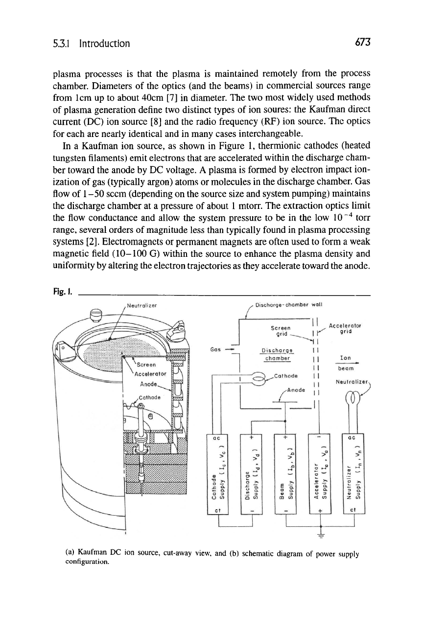
In a Kaufman ion source, as shown in Figure 1, thermionic cathodes (heated
tungsten filaments) emit electrons that are accelerated within the discharge cham-
ber toward the anode by DC voltage. A plasma is formed by electron impact ion-
ization of gas (typically argon) atoms or molecules in the discharge chamber. Gas
flow of
1
-50 seem (depending on the source size and system pumping) maintains
the discharge chamber at a pressure of about 1 mtorr. The extraction optics limit
the flow conductance and allow the system pressure to be in the low 10""^ torr
range, several orders of magnitude less than typically found in plasma processing
systems [2]. Electromagnets or permanent magnets are often used to form a weak
magnetic field (10-100 G) within the source to enhance the plasma density and
uniformity by altering the electron trajectories as they accelerate toward the anode.
Flg.l.
L
Discharge-chamber wall
Screen
grid -,
Gas —• Discharge
chamber
1
' ' Accelerator
I y^ grid
Ion
:S-'
Cathode
Anode
beam
Neutralizer>,
(a) Kaufman DC ion source, cut-away view, and (b) schematic diagram of power supply
configuration.
