Hoffman D.M., Singh B., Thomas J.H. (Eds). Handbook of Vacuum Science and Technology
Подождите немного. Документ загружается.

674
Rg.2.
Chapter 5.3: Ion Beam Technology
GAS
ACCEI£RATOR
GRID
NEUTRAUZER
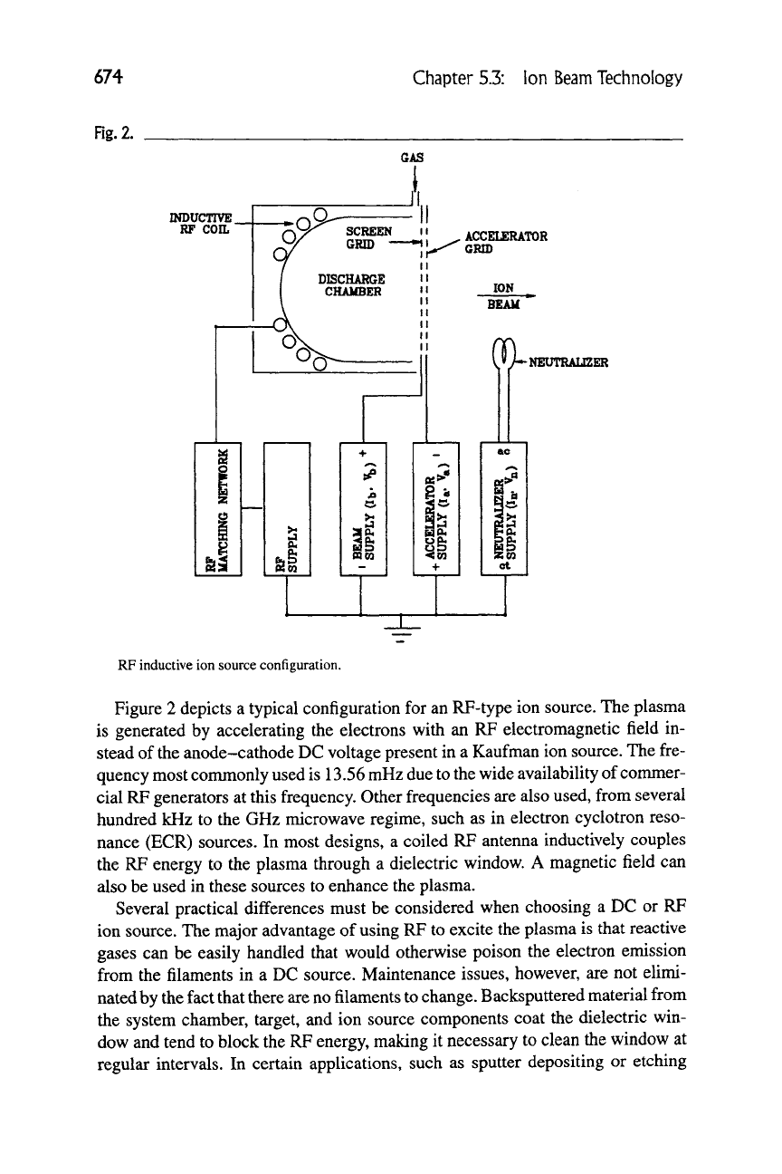
RF inductive ion source configuration.
Figure 2 depicts a typical configuration for an RF-type ion source. The plasma
is generated by accelerating the electrons with an RF electromagnetic field in-
stead of the anode-cathode DC voltage present in a Kaufman ion source. The fre-
quency most conmionly used is 13.56 mHz due to the wide availability of commer-
cial RF generators at this frequency. Other frequencies are also used, from several
hundred kHz to the GHz microwave regime, such as in electron cyclotron reso-
nance (ECR) sources. In most designs, a coiled RF antenna inductively couples
the RF energy to the plasma through a dielectric window. A magnetic field can
also be used in these sources to enhance the plasma.
Several practical differences must be considered when choosing a DC or RF
ion source. The major advantage of using RF to excite the plasma is that reactive
gases can be easily handled that would otherwise poison the electron emission
from the filaments in a DC source. Maintenance issues, however, are not elimi-
nated by the fact that there are no filaments to
change.
Backsputtered material from
the system chamber, target, and ion source components coat the dielectric win-
dow and tend to block the RF energy, making it necessary to clean the window at
regular intervals. In certain applications, such as sputter depositing or etching
5.3.1 Introduction 675
metals, the amount of backsputtered metal can easily make maintenance on an RF
ion source equal to if not exceeding that of a DC source.
Once a plasma has been formed, two or three closely spaced grids are generally
used to extract a controlled beam. The grid material is typically pyrolytic graphite
or molybdenum, depending on the application. Graphite is generally used in a re-
active gas environment and for smaller ion sources, but should be avoided if oxy-
gen will be used, since the graphite will be etched quickly. The high strength and
stiffness of molybdenum makes it the material of choice for larger sources in a
production environment. The grids can be configured for a divergent, coUimated,
or focused ion beam by offsetting the hole patterns in the grids and, in the case of
molybdenum, dishing the grids in a concave or convex manner to provide the de-
sired beam shape. Divergent and collimated grids are selected for etching appli-
cations where beam uniformity is of prime concern. Focused grids are generally
chosen for ion beam deposition applications where the beam is to be focused and
contained on a target.
The two figures of merit that determine the major processing characteristics of
an ion beam are the beam energy and current. The kinetic energy of the ion beam
is the potential difference between the plasma and ground, which is set by the
beam voltage power supply. The beam current or ion flux is determined by the in-
tensity of the plasma in the source. In the DC source the plasma density is con-
trolled by the discharge current, and in the RF source it is controlled by the RF
power. It is important to note that these two parameters can be independently var-
ied over a wide range.
5.3.1.1
Gridless Sources
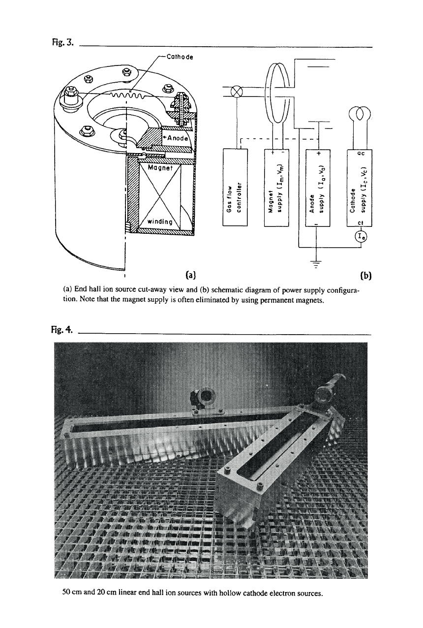
Another type of broad beam ion source that is used mainly in ion-assisted deposi-
tion and precleaning applications is the end hall ion source [9] shown in Figure 3.
This type of ion source was originally developed in the former Soviet Union's space
propulsion research program to overcome the current density limitations at low
energies imposed by the extraction optics in a gridded ion source. The accelerat-
ing potential for the ions in the end hall source is developed by a circulating elec-
tron current in a magnetic field. A high-curie point permanent magnet provides
the magnetic field in current conmiercial designs, allowing the source and power
supply to be simple and rugged. The electron source can be either a heated tung-
sten filament or a hollow-cathode-type electron source, which is discussed later.
Typical beam characteristics are a highly divergent (~45° half angle) beam,
high current densities (several mA/cm^ at the source), and low ion energies (30-
120 eV). In addition to the circular end hall sources as shown in Figure 3, the
sources can be constructed in a linear configuration for use in continous feed ap-
plications. A 20 cm and 50 cm linear source are shown in Figure 4 and sources up
to
1
meter in length are commercially available.
Rg.3.
Cathode
W
(b)
(a) End hall ion source cut-away view and (b) schematic diagram of power supply configura-
tion.
Note that the magnet supply is often eliminated by using permanent magnets.
Fig.
4.
50 cm and 20 cm linear end hall ion sources with hollow cathode electron sources.
5.3.1 Introduction (>n
53.1.2 Ion Beam Neutralization
As the ion beam transits from the ion source to the target or substrate, there is an
intense space charge repulsion between the positive ions which will tend to dis-
rupt the beam. By putting a source of electrons nearby, a net charge of zero per
unit volume (charge neutralization) can be achieved in the beam; ie., equal densi-
ties of positive and negative charges. In addition to charge neutralization of the
beam, sufficient electrons must be supplied to achieve total current neutralization
at the substrate, i.e., equal arrival rates of positive and negative charges. If the tar-
get is an insulator or is electrically isolated from ground, insufficient current neu-
tralization will result in positive voltages building up on the surface. If an inten-
tional source of electrons is not provided, the surrounding surfaces in the system
will supply them in the form of short arcs and flashes, which can be observed
through a viewport, if available. This uncontrolled arcing can cause damage, ei-
ther directly if the arc is from the target or substrate, or indirectly when particles,
ejected from an arc, land on sensitive surfaces. Voltage fluctuations in the ion
beam due to inadequate neutralization can cause variations in the process during
the run and from run to run. To assure that neutralization is occurring, the elec-
tron emission current is generally set to a value of about 10% over the ion beam
current set point.
An external source of electrons is only necessary for the gridded ion sources.
Since the electron emitter for the gridless ion sources is external by design, it sup-
plies the electrons to both form the plasma and to neutralize the ion beam.
Several methods for neutralizing the ion beam are commonly used. The sim-
plest approach is to immerse in the ion beam a heated tungsten filament that will
thermionically emit enough electrons to cancel out the positive charges in the
beam. The placement or symmetry of the filament in the beam is not critical,
since the mobility of the electrons is orders of magnitude larger than the more
massive ions. The filament is sputtered by the ion beam, which limits its lifetime,
and the sputtered filament material may present a problem if contamination of a
depositing film is critical. In this case two other types of neutralizers are avail-
able,
the plasma bridge and the hollow cathode neutralizers.
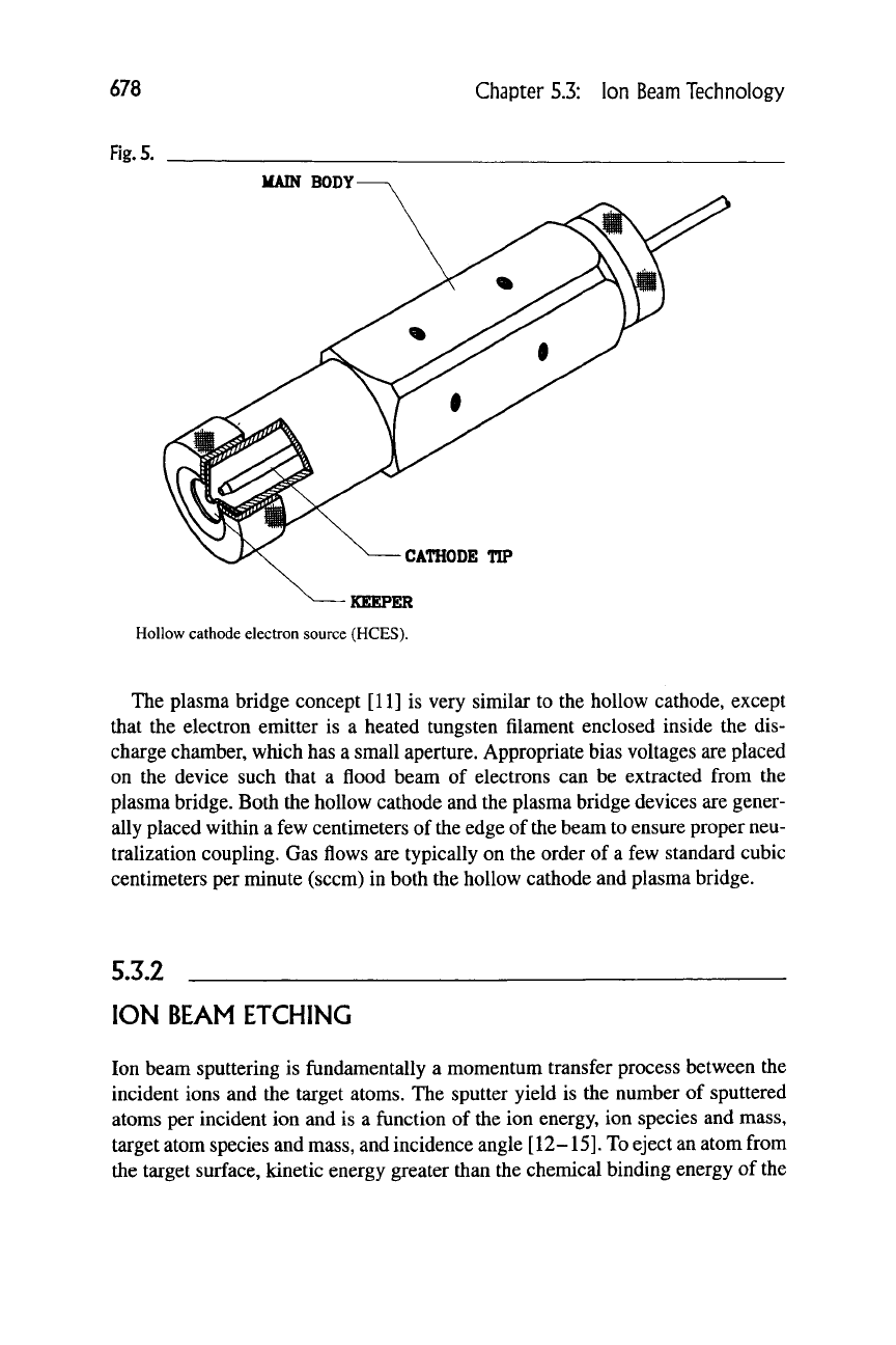
In the hollow cathode [10], the electron emission is from a low function work
function insert as shown in Figure 5. The emission is primarily thermionic due to
the high temperature of the insert, although it is usually enhanced by strong elec-
tric fields at the insert surface. The insert is heated by ion bombardment from the
internal plasma. The plasma couples to the surroundings through the small open-
ing at the end of the hollow cathode. The internal pressure to the hollow cathode
is in the
1
-10 torr range, and the electron emission surface is sensitive to contam-
ination, thus the gas flowing through the tip must be a high-purity noble gas such
as argon, krypton, or xenon.
678
Chapter S.3:
Ion
Beam Technology
Fig.
5.
MAIN BODY
CATHODE TIP
-KEEPER
Hollow cathode electron source (HCES).
The plasma bridge concept [11] is very similar to the hollow cathode, except
that the electron emitter is a heated tungsten filament enclosed inside the dis-
charge chamber, which has a small aperture. Appropriate bias voltages are placed
on the device such that a flood beam of electrons can be extracted from the
plasma bridge. Both the hollow cathode and the plasma bridge devices are gener-
ally placed within a few centimeters of the edge of the beam to ensure proper neu-
tralization coupling. Gas flows are typically on the order of a few standard cubic
centimeters per minute (seem) in both the hollow cathode and plasma bridge.
5.3.2
ION BEAM ETCHING
Ion beam sputtering is fundamentally a momentum transfer process between the
incident ions and the target atoms. The sputter yield is the number of sputtered
atoms per incident ion and is a function of the ion energy, ion species and mass,
target atom species and mass, and incidence angle [12-15]. To eject an atom from
the target surface, kinetic energy greater than the chemical binding energy of the
5.3.2 Ion Beam Etching f>7^
atom must be imparted to the atom. Ion energy thresholds to impart this amount
of energy range from 10 to 100 eV [13], depending on the material. The sputter
yield from material to material follows the trend of binding energy within the pe-
riodic table and increases with ion beam energy up to about 10 keV where im-
plantation starts to dominate [12].
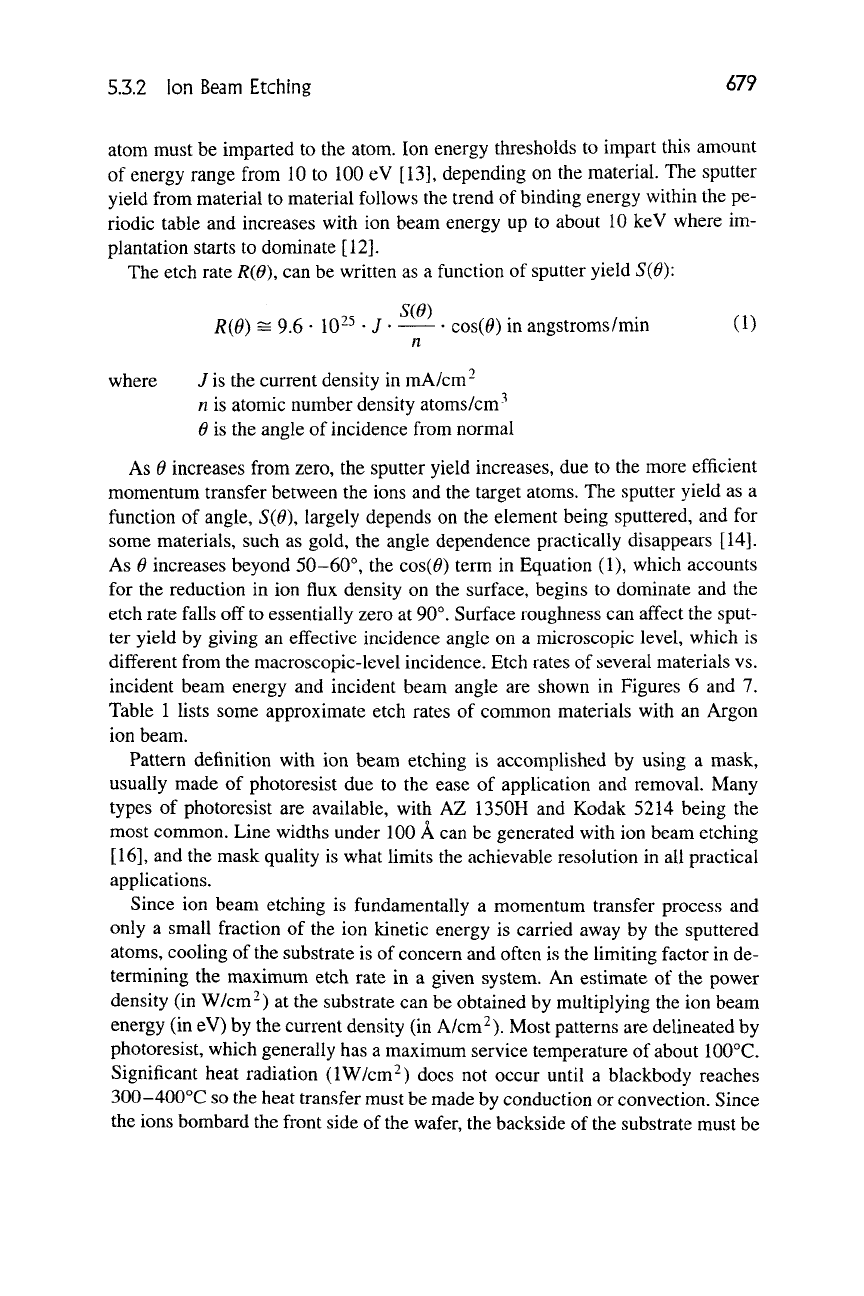
The etch rate R{6), can be written as a function of sputter yield S{6)\
R{d) = 9.6
•
10-^
•
J ' — ' cos(0) m angstroms/nun (1)
n
where J is the current density in mA/cm"
n is atomic number density atoms/cm^
6 is the angle of incidence from normal
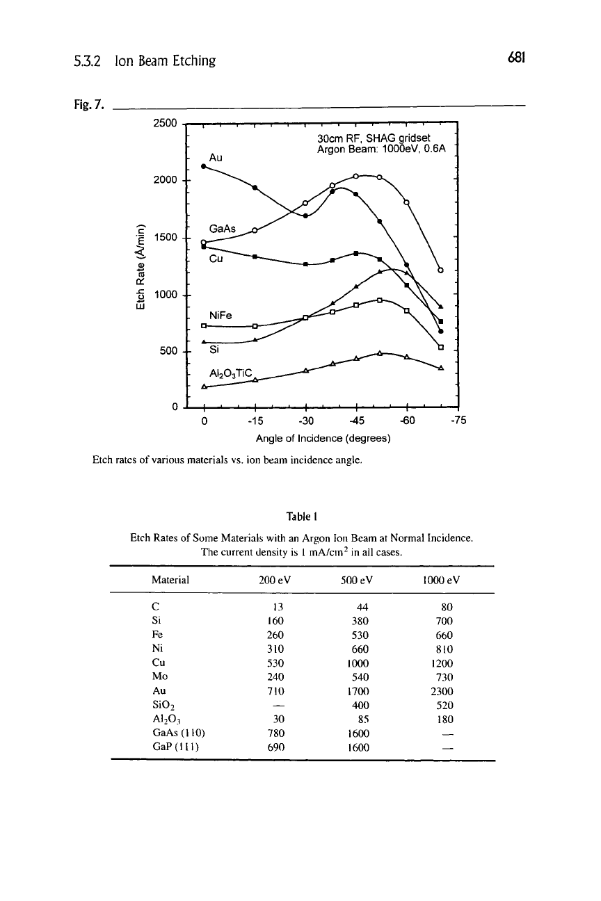
As 6 increases from zero, the sputter yield increases, due to the more efficient
momentum transfer between the ions and the target atoms. The sputter yield as a
function of angle, S(6), largely depends on the element being sputtered, and for
some materials, such as gold, the angle dependence practically disappears [14].
As 0 increases beyond 50-60°, the cos(^) term in Equation (1), which accounts
for the reduction in ion flux density on the surface, begins to dominate and the
etch rate falls off to essentially zero at 90°. Surface roughness can affect the sput-
ter yield by giving an effective incidence angle on a microscopic level, which is
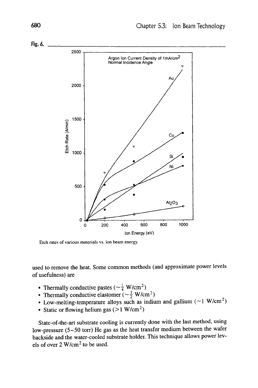
different from the macroscopic-level incidence. Etch rates of several materials vs.
incident beam energy and incident beam angle are shown in Figures 6 and 7.
Table 1 lists some approximate etch rates of common materials with an Argon
ion beam.
Pattern definition with ion beam etching is accomplished by using a mask,
usually made of photoresist due to the ease of application and removal. Many
types of photoresist are available, with AZ 1350H and Kodak 5214 being the
most common. Line widths under 100 A can be generated with ion beam etching
[16],
and the mask quality is what limits the achievable resolution in all practical
applications.
Since ion beam etching is fundamentally a momentum transfer process and
only a small fraction of the ion kinetic energy is carried away by the sputtered
atoms, cooling of the substrate is of concern and often is the limiting factor in de-
termining the maximum etch rate in a given system. An estimate of the power
density (in W/cm-) at the substrate can be obtained by multiplying the ion beam
energy (in eV) by the current density (in A/cm^). Most patterns are delineated by
photoresist, which generally has a maximum service temperature of about 100°C.
Significant heat radiation (IW/cm-) docs not occur until a blackbody reaches
300-400°C so the heat transfer must be made by conduction or convection. Since
the ions bombard the front side of the wafer, the backside of the substrate must be
680
Fig.
6.
Chapter 5.3: Ion
Beam
Technology
2500
2000 ]
^ 1500
A
E
"J 1000 ]
500
A
Argon Ion Current Density of ImA/cm^
Normal Incidence Angle
0 200 400 600 800
Ion Energy (eV)
Etch rates of various materials vs. ion beam energy.
1000
used to remove the heat. Some common methods (and approximate power levels
of usefulness) are
• Thermally conductive pastes (~ j W/cm^)
• Thermally conductive elastomer (~ j W/cm-)
• Low-melting-temperature alloys such as indium and gallium (~1 W/cm )
• Static or flowing helium gas (>1 W/cm^)
State-of-the-art substrate cooling is currently done with the last method, using
low-pressure (5-50 torr) He gas as the heat transfer medium between the wafer
backside and the water-cooled substrate holder. This technique allows power lev-
els of over 2 W/cm^^ to be used.
5.3.2 Ion Beam Etching
681
Fig.
7.
2500
2000 4-
T—I 1 I I I I I ' '
30cm RF, SHAG gridset
Argon Beam: lOOOeV, 0.6A
H—^
0 -15 -30 -45 -60
Angle of Incidence (degrees)
Etch rates of various materials vs. ion beam incidence angle.
-75
Table 1
Etch Rates of Some Materials with an Argon Ion Beam at Normal Incidence.
The current density is I mA/cm^ in all cases.
Material
C
Si
Fe
Ni
Cu
Mo
Au
Si02
AI2O3
GaAs(llO)
GaP(lll)
200
eV
13
160
260
310
530
240
710
—
30
780
690
500
eV
44
380
530
660
1000
540
1700
400
85
1600
1600
1000
eV
80
700
660
810
1200
730
2300
520
180
—
—
682 Chapter 5.3: Ion
Beam
Technology
The ions do not stop at the surface but penetrate approximately 20-100 A deep
in the energy range 100-1000 eV. Damage in ion-etched semiconductors has
been studied [17-19] in Si, GaAs, and other electronic materials, and damage
thresholds ranging from 50 eV up to several hundred eV have been found. Al-
though generally detrimental in semiconductor devices, the damaged layer on the
surface can sometimes be beneficial in forming good ohmic contacts.
The most common gas species used for nonreactive ion beam etching is argon,
due to the combination of low cost and relatively high atomic mass. Etching rates
can be increased for some materials by using a reactive gas to generate the plasma
and extracting the ionized reactants. This process is termed reactive ion beam
etching (RIBE). The reactive gas can also be introduced near the substrate, chemi-
sorbed onto the surface, and an inert ion beam can provide the energy to complete
the chemical reaction. This is referred to as chemically assisted ion beam etching
(CAIBE). In a purely chemical etching system, compound materials often cannot
be successfully etched, because of the widely different reactivity and vapor pres-
sures of
the
component elements. Complex gas mixtures are often used in reactive
ion etching (RIE) plasmas to achieve the desired etch selectivity and anisotropy
[20].
In ion beam etching, there is always a physical component to the material re-
moval mechanism, and many of the complications found in RIE processing dis-
appear.
Etch rate increases of 50:1 over inert ion milling can be achieved on a variety
of materials using the RIBE and CAIBE techniques [21-29]. The benefits of
chemically enhanced ion milling such as higher rates, etch selectivity, and profile
control have to be weighed against the added cost and complication of handling
reactive gases such as CI2 and CF4 as opposed to pure argon. It has been shown
that submicron features in GaAs can be etched with aspect ratios of over
40:1
us-
ing an Argon ion beam and
CI2
gas introduced at the substrate surface
[25].
CAIBE
techniques appear promising [30,31] in efforts to etch III-V nitrides, of interest
in new optoelectronic devices, where chemical and RIE methods have met with
resistance.
Argon ion beam etching has shown some unique capabilities in optical appli-
cations. These range from formation of microlenses on InP and Si for use in infra-
red devices [32,33] to ion beam "figuring" of ultra-high-quality optical surfaces
over large areas where the limits of mechanical polishing are met [34].
Ion milling is also useful for use in etching of complex compounds such as
LiNbO^ waveguides [35] and Y-Ba-Cu-0 superconductor devices [36,37] where
it is difficult to determine the optimum process in a pure chemical etch. In addi-
tion to compound materials, ion beam milling is often used to etch multilayer
stacks such as Ti/Pt/Au in a single process step without requiring parameters
such as gas mixture to change from one material to the next.
A major application of ion beam sources is in the "precleaning" of substrates
prior to a deposition process. The ion source allows the highly controlled removal
of the top few monolayers on a surface that may contain impurities and/or con-
5.3.3 Ion Beam Sputter Deposition
683
Fig.
8.
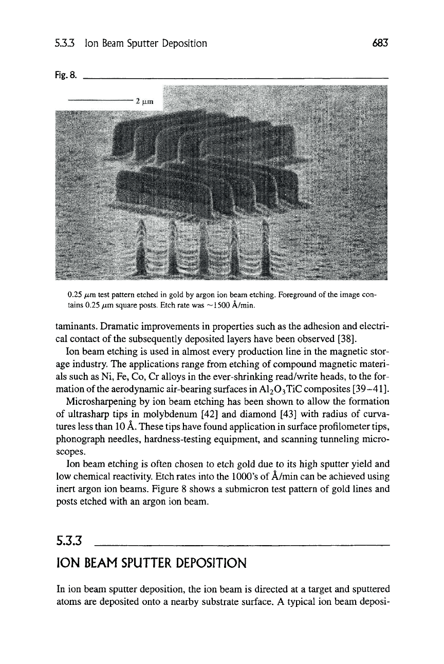
0.25
/mm
test pattern etched in gold by argon ion beam etching. Foreground of the image con-
tains 0.25
/u-m
square posts. Etch rate was ~1500 A/min.
taminants. Dramatic improvements in properties such as the adhesion and electri-
cal contact of the subsequently deposited layers have been observed [38].
Ion beam etching is used in almost every production line in the magnetic stor-
age industry. The applications range from etching of compound magnetic materi-
als such as Ni, Fe, Co, Cr alloys in the ever-shrinking read/write heads, to the for-
mation of the aerodynamic air-bearing surfaces in Al203TiC composites [39-41].
Microsharpening by ion beam etching has been shown to allow the formation
of ultrasharp tips in molybdenum [42] and diamond [43] with radius of curva-
tures less than
10
A. These tips have found application in surface profilometer tips,
phonograph needles, hardness-testing equipment, and scanning tunneling micro-
scopes.
Ion beam etching is often chosen to etch gold due to its high sputter yield and
low chemical reactivity. Etch rates into the lOOO's of A/min can be achieved using
inert argon ion beams. Figure 8 shows a submicron test pattern of gold lines and
posts etched with an argon ion beam.
5.3.3
ION BEAM SPUTTER DEPOSITION
In ion beam sputter deposition, the ion beam is directed at a target and sputtered
atoms are deposited onto a nearby substrate surface. A typical ion beam deposi-
