Hawkes P.W., Spence J.C.H. (Eds.) Science of Microscopy. V.1 and 2
Подождите немного. Документ загружается.

970 P. Sutter
technique, a historic overview may also be of limited value. Hence, I
have tried to identify representative examples in the current literature,
which are discussed briefl y to illustrate the different uses of STM. The
connection to historic developments can in most cases be made easily
via literature references. For a more in-depth discussion of basic con-
cepts and application examples, several dedicated monographs on
STM and other scanning probe techniques (Chen, 1993; Wiesendanger,
1994; Güntherodt and Wiesendanger, 1992; Bonnell, 2001) represent an
invaluable resource.
This chapter is organized as follows. In Section 2 basic principles of
STM imaging are introduced, and the imaging methodology as well
as practical and instrumentation requirements are discussed. The
approach taken in surface imaging by STM is illustrated by the example
of silicon surfaces. Section 3 highlights an application of STM that has
gained ever-increasing importance: atomic scale spectroscopy. It pro-
vides a survey of the spectroscopy capabilities of STM, and introduces
a variety of techniques for local spectroscopy and spectroscopic
imaging. In addition, pathways toward obtaining chemical and element
specifi city at the atomic scale—traditionally a weakness of STM—are
discussed. The extension of the operating conditions of STM to high
and low temperatures has opened up new avenues of investigation.
Variable temperature STM of dynamic surface processes as well as
atom and molecule manipulation at cryogenic temperatures are the
topics of Section 4. Section 5 discusses STM imaging and spectros-
copy on subsurface structures, using ballistic electrons to probe
buried interfaces or cross-sectional STM on cleavage faces of III–V
semiconductors to image embedded nanostructures. The chapter con-
cludes with a brief discussion of STM image simulation techniques in
Section 6.
2 Basic Principles of STM Imaging
2.1 Elastic Vacuum Tunneling and
Scanning Tunneling Microscopy
STM is based on the vacuum tunneling of electrons between two
solids, one of which is a sharp tip and the other a sample. To remove
an electron from a solid and bring it into vacuum with zero kinetic
energy requires energy equal to the work function φ = E
Vac
− E
F
, i.e., the
difference between the vacuum level, E
vac
, and the Fermi energy of the
material, E
F
. To move an electron from one solid to another, it has to
cross the same vacuum barrier. If the two solids are separated by a
microscopic distance of the order of the decay length of electronic
states into the vacuum (typically about 1–5 nm), electrons can cross the
barrier by quantum mechanical tunneling (Figure 15–1).
If, say, two metals are brought to within tunneling distance, a rapid
charge transfer takes place between them until an equilibrium state is
established in which their Fermi levels are aligned. Once in equilib-
rium, no net charge is transferred on average. Consider now a slightly
modifi ed situation, in which metal A is biased relative to B by applying
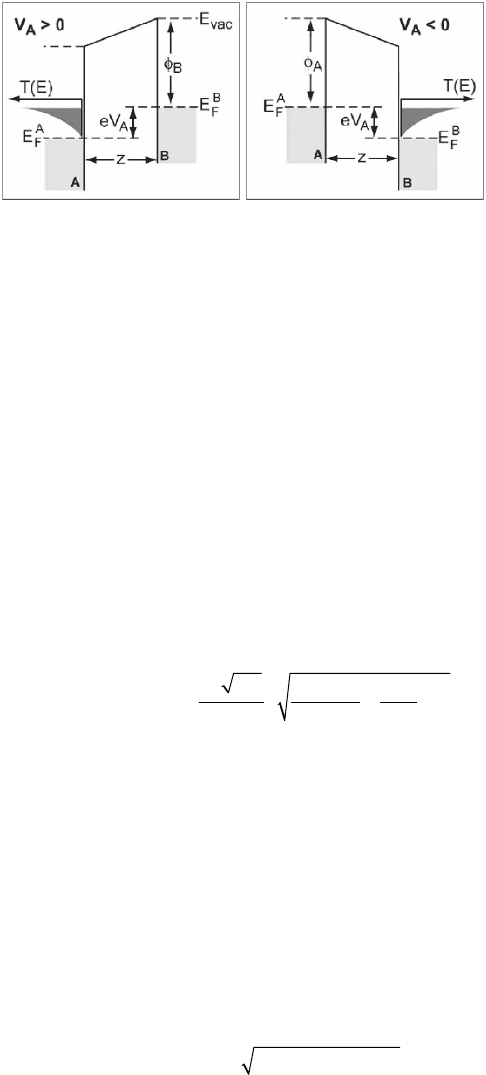
Chapter 15 Scanning Tunneling Microscopy in Surface Science 971
a voltage, V
A
. The bias offsets the Fermi energies on either side of the
vacuum barrier by eV
A
. Under steady-state conditions, this potential
difference establishes a net tunneling current, I, between A and B.
In a simple planar tunneling model using the Wentzel–Kramers–
Brillouin (WKB) approximation, the tunneling current is given by an
integral over the energy range between the Fermi energies on either
side of the vacuum gap,
IEEeVTEeVdE
eV
=
(
)
−
(
)
(
)
∫
ρρ
AAA
A
Β
0
, (1)
where ρ
A
and ρ
B
denote the local density of states at energy E at the
surface of A and B, respectively, and T(E, eV
A
) is the tunneling transmis-
sion probability for electrons with energy E and applied bias V
A
:
TEeV
zm eV
E,exp
A
AB A
(
)
=−
+
+−
22
22
φφ
(2)
Here, φ
A,B
are the work functions of the two solids, z is their separation,
and m is the mass of the electron. Evaluation of T for positive (V
A
> 0)
and negative bias (V
A
< 0) shows that the transmission probability is
highest for electrons at the Fermi energy of the material that is nega-
tively biased, and falls off exponentially for lower energies down to a
lower cutoff at the Fermi energy of the positively biased electrode. This
general observation has important consequences in tunneling spec-
troscopy and spectroscopic imaging, as discussed in Section 3.
The tunneling current depends strongly on the separation, z, between
the two solids. To illustrate this fact, we simplify Eq. (1) by assuming
constant densities of states, independent of energy. In the limit of low
bias voltage, V
A
/φ
A,B
<< 1, the tunneling current is then given by
IV m z=−+
(
)
(
)
ρρ φ φ
ABA A B
exp /2
2
(3)
i.e., it depends exponentially on the separation. It is from this strong z
dependence of the tunneling current that STM derives its exquisite
height resolution, typically of the order of 0.1 pm, or below 1/100 mono-
layer for most solids.
Figure 15–1. Band diagrams (energy vs. distance along the tunneling direc-
tion) for vacuum tunneling between two metal electrodes, A and B.
972 P. Sutter
In actual STM imaging, an atomically sharp tip is used to obtain
laterally confi ned tunneling at a well-defi ned position of a sample. A
piezoelectric positioning element controls the in-plane (x, y) position
and height (z) of the tip with picometer resolution. While a constant
bias voltage is applied between sample and tip, the tip is scanned in a
line-by-line fashion to continuously change the tunneling position and
build up an image of a chosen area of interest on the sample. The strong
dependence of the tunneling current on the tip–sample separation can
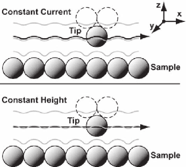
be used for two basic modes of STM imaging: constant-current and
constant-height imaging (Figure 15–2).
In constant-current imaging, the tunneling current is measured at
each pixel of the scan and is compared with a chosen current set point.
Deviations between the measured tunneling current and the set point
are corrected by applying an appropriate voltage to the z-piezo, thus
adjusting the tip–sample separation. This feedback mechanism main-
tains a constant tunneling current during the scan, while the trajectory
z(x, y) followed by the tip is used to generate a map of the sample
surface or, more accurately, a map of a particular charge density contour
above the surface.
In constant-height mode, the tip height is not modifi ed during the
scan. The tunneling current is again measured at each image pixel, but
is now used directly as a representation of the sample surface via a
current map, I(x, y). The current maps represent a cut through charge
density contours in the plane in which the tip is scanned above the
sample. Obviously, since the tip–sample separation is uncontrolled
during the scan, constant-height imaging is limited to samples with
low corrugation and/or small scan sizes. A more practical implementa-
tion of constant-height STM uses a slow feedback system to adjust the
tip–sample separation on time scales that are long compared to the
residence time at each pixel, thus compensating for sample surface
topography or sample tilt. As the current comparison and tip z cor-
rection are eliminated and only the tunneling current is measured,
data acquisition can be faster than in constant-current imaging. The
constant-height mode is thus preferred for fast STM image acquisition.
Figure 15–2. Schematic tip
trajectory for STM imaging in
constant current and constant
height mode.
Chapter 15 Scanning Tunneling Microscopy in Surface Science 973
2.2 Inelastic Vacuum Tunneling
The above considerations assumed elastic tunneling between two
materials, e.g., a sharp tip and the sample. In this case, the energy of a
tunneling electron is conserved in the transit through the vacuum
barrier. Only inside the opposite electrode the electron thermalizes
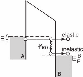
to the Fermi energy by phonon emission. Tunneling electrons can,
however, undergo inelastic scattering during the tunneling process.
Vibrational modes of molecules adsorbed on the sample surface, for
example, can be excited by inelastic scattering of a small fraction of the
tunneling electrons (Figure 15–3).
The onset of inelastic tunneling at characteristic energies can then
be detected and used as a fi ngerprint to identify individual molecular
bonds. Such STM-based single molecule vibrational spectroscopy will
be discussed in Section 3. In addition, controlled amounts of energy
can be deposited locally into individual adsorbates, important for
the manipulation of adsorbed atoms or molecules, as discussed in
Section 4.
2.3 Practical Requirements: Tips, Samples, and
Operating Environment
Obtaining a highly localized tunneling contact requires very sharp
probe tips, ideally terminated by a single atom or a small cluster.
D-band metals (e.g., W) or alloys (PtIr) are generally thought to be
superior for obtaining high spatial resolution due to the strongly direc-
tional nature of the d-wave function. However, atomic resolution has
also been obtained with Au tips, i.e., tip materials with primarily s-
electrons at the Fermi level.
Electrochemically etched tungsten wires are often used for high-
resolution STM in vacuum, while less reactive PtIr or Au tips are
preferred for imaging under ambient conditions. Sharp W tips are
produced by electrochemical etching in ∼2 M KOH or NaOH solution,
using a stainless steel or Pt foil as a counter electrode. dc or ac etching
at typical bias voltages of 5–10 V can be used. Preferential etching at
the meniscus of the solution leads to a tapering of the immersed wire,
causing one end to eventually break off. To prevent further etching that
would blunt the tip apex, an electronic circuit detects the break-off
Figure 15–3. Band diagrams for elastic
and inelastic electron tunneling.
974 P. Sutter
current and switches the bias to zero within a few microseconds.
Etched tips are rinsed in deionized water to remove traces of the etch
solution, and loaded into ultrahigh vacuum (UHV). Contaminants and
surface oxide are desorbed from the tip by a heat treatment in UHV
prior to mounting the tip into the STM. Electron beam bombardment
of the tip apex provides an effi cient local cleaning of the thin part of
the tip, and the applied electric fi eld in this procedure may lead to an
additional tip sharpening (Kuk and Silverman, 1986). Alternative tip
cleaning and modifi cation techniques while in tunneling contact
involve voltage pulses of the order of 4–10 V while scanning the sample,
or tip forming in the fi eld emission regime (i.e., at tip–sample large
separation) with applied bias voltages between 10 and 100 V and cur-
rents of several nA. Ideally, the atomic confi guration of the tip would
be characterized by fi eld ion microscopy (FIM) prior to its use in the
STM. Attempts have been made to combine FIM with STM. However,
in practice such efforts are of limited benefi t since tip changes occur
frequently during scanning, rendering a complete characterization of
the tip impractical.
To allow the controlled biasing of tip and sample, and to prevent
charging, conventional direct current STM is limited to metal or semi-
conductor samples. Alternating current STM (Kochanski, 1989) has
been demonstrated on insulators and organic layers, but is not widely
used. Clean and ordered crystalline surfaces with low surface rough-
ness are preferred for most studies, in particular for atomic-resolution
imaging. Reactive semiconductor or metal surfaces are best prepared
and imaged in UHV, but metal surfaces are also prepared and imaged
routinely in electrolytes (Gewirth and Niece, 1997). In vacuum, sample
preparation often involves a thermal cleaning step to remove contami-
nants. Flash cleaning to 1200°C for a brief period of time (few seconds)
while keeping the vacuum in the low 10
−9
torr range removes the native
oxide and provides atomically clean Si samples with a low density of
SiC contaminants. Metal surfaces (e.g., Cu, Al, Pt, Au), and some semi-
conductors (e.g., Ge) are prepared in a two-step procedure involving
repeated cycles of Ar
+
ion sputtering and annealing. In refractory
metals such as Ru, C contamination is removed by many (several
hundred) cycles of oxygen adsorption near room temperature and
fl ashing to 1500°C. In situ cleavage can be a very effective method for
preparing sample surfaces that cannot be sputtered or heated to high
temperatures. Samples best prepared by cleavage include III–V com-
pound semiconductors (GaAs, InAs), as well as high-T
C
superconduc-
tors (Yba
2
Cu
3
O
7−x
, BiSr
3
Cu
2
O
8+x
). In situ cleavage is also the preparation
method of choice for cross-sectional STM (see Section 5), commonly
performed on (110) cleavage planes of III–V semiconductors. Bulk insu-
lating metal oxides, most prominent among them TiO
2
, can be imaged
successfully by STM following Ar
+
ion sputtering and annealing, which
generates oxygen vacancies and renders the surface region suffi ciently
conductive for stable STM imaging. Au and highly oriented pyrolitic
graphite (HOPG) are among the few materials on which atomic resolu-
tion is obtained under ambient conditions. Well-ordered, (111) oriented
surfaces of Au single crystals and thin fi lms on mica can be prepared
Chapter 15 Scanning Tunneling Microscopy in Surface Science 975
by fl ame annealing in air (Robinson et al., 1992). Preparation of layered
materials, notably HOPG, is particularly simple. It involves the removal
of bundles of graphene layers by adhesive tape from the crystal. Since
the exposed graphene sheet has no dangling bonds and is very inert,
such samples can be imaged with atomic resolution in air for extended
time periods.
For many materials, in particular metals and alloys, electrochemical
STM is a powerful alternative to imaging in UHV. In this environment,
almost the entire portion of the tip that is immersed in the solution
must be coated by an insulating layer (e.g., wax or glass) to minimize
the faradaic (i.e., ionic) current, which is typically much larger than the
tunneling current and would otherwise dominate the measured signal.
Only a small fraction near the apex of the tip remains uncoated to
allow for tunneling between the tip and sample.
2.4 STM Instrumentation
In tunneling contact the probe tip is only a distance of the order of
1 nm away from the sample. As the tunneling current is exponentially
sensitive on the tip–sample separation, any mechanical vibrations of
the tip relative to the sample have to be minimized. To this end, a two-
fold strategy is commonly pursued. The microscope head itself is built
as compact and stiff as possible by closely integrating sample and tip
on a rigid platform. This results in a high resonance frequency for
oscillations of the tip relative to the sample. In addition, the entire
microscope is isolated mechanically from outside vibration sources,
e.g., by suspending it on soft extension springs or long bungy cords.
The overall goal is to achieve a maximal mismatch between the mech-
anical modes of a soft suspension system and the high resonance fre-
quency of the stiff microscope head. In addition, effi cient vibration
damping is required, which can be achieved by magnetically induced
eddy currents. The springs used in many suspension systems have
their own mechanical modes that can be damped by polymer strips
woven into their coils. Direct coupling of acoustic noise into the micro-
scope, fi nally, is a problem that is best solved by operating the STM in
vacuum (Figure 15–4).
A few additional components are part of any practical tunneling
microscope. A coarse approach mechanism has to be in place, which
moves the tip from an initial distance of several millimeters into
tunneling range without making physical contact with the sample.
Although this has been achieved by mechanical approach mechanisms
(Smith and Binnig, 1986), piezoelectric driven stick-slip motors are now
preferred since they allow the entire coarse approach to be performed
automatically under computer control. For the positioning and scan-
ning of the tip during STM imaging, a segmented piezoelectric tube
scanner is used (Binnig and Smith, 1986). By applying high voltages to
the individual segments, the scanner is independently actuated in the
(x, y) plane parallel to the sample surface and along the perpendicular
z axis with little crosstalk. The tunneling current in the pA to nA
range is converted into a voltage by a sensitive, low-noise amplifi er
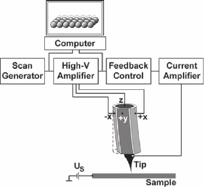
976 P. Sutter
with adjustable transconductance of 10
7
–10
10
V/A, whic h provides the
input signal for the tunneling current feedback electronics. Modern
STM controllers typically use digital feedback and scan modules imple-
mented by specifi c software programs running on fast digital signal
processor (DSP) chips. The measured analog tunneling current signal
is digitized using an analog-to-digital (A/D) converter, and is com-
pared with the current set point by the feedback program on the
DSP. Necessary corrections in the tip height z are computed, and are
converted into analog voltages by digital-to-analog (D/A) converters.
These voltages may be amplifi ed further by a high-voltage amplifi er
stage to levels suitable to drive the tube scanner. The scan signal, i.e.,
independent voltage ramps driving the piezo scanner along the in-
plane x and y directions, is also generated digitally on a DSP, followed
by conversion and amplifi cation steps analogous to those of the z
signal. A program running on a host computer and communicating
with the DSP, fi nally, acquires, displays, and stores the measured tip
trajectory z(x, y) (in constant-current imaging) or position-dependent
tunneling current I(x, y) (in constant-height mode).
2.5 STM Imaging: Application Examples
High-resolution imaging of surface structure is probably the most
widespread application of STM. As a direct imaging technique, STM
has added signifi cantly to the diffraction techniques used traditionally
to determine the structure of clean and adsorbate covered surfaces.
Examples of typical applications include the determination of the
structure of reconstructed surfaces of clean semiconductors, for
instance vicinal Si surfaces (Erwin et al., 1996) and oxides, such as TiO
2
(Diebold, 2003), and of adsorbate-induced reconstructions on metals
Figure 15–4. Schematic illustration of the various components of an STM
system, including piezoelectric tube scanner for tip positioning, and con-
trol electronics (current amplifi er, feedback, scan generator, high-voltage
amplifi er).
Chapter 15 Scanning Tunneling Microscopy in Surface Science 977
(e.g., O/Ru(0001); Meinel et al., 1997); the mapping of the evolution
of surface morphology during epitaxial growth (e.g., metal epitaxy;
Chambliss et al, 1995), etching (Boland and Weaver, 1998), and ener-
getic particle bombardment (e.g., electrons on Si; Nakayama and
Weaver, 1999); and the imaging and structural identifi cation of non-
periodic structures such as surface defects, steps, as well as surface-
supported solid (e.g., silicide nanowires on Si; Chen et al., 2000)
and molecular nanostructures [e.g., molecular rotors on Cu(100);
Gimzewski et al., 1998]. Although electrically conducting samples are
a prerequisite for stable tunneling, high-resolution imaging is feasible
on ultrathin insulating fi lms (for a recent review, see Schintke and
Schneider, 2004) and self-assembled organic monolayers [e.g., alkane-
thiol monolayers on Au(111); Cygan et al., 1998) supported by metal
substrates.
In view of the large number of materials systems to which STM has
been applied, a comprehensive survey would be beyond the scope of
this chapter. Instead, we discuss in some detail recent contributions of
STM imaging to one specifi c material: silicon.
2.5.1 STM Imaging—Silicon Surfaces
Due to the important role of Si in electronics, extensive STM studies
on the structure of clean Si surfaces with different orientation have
contributed to making Si one of the best-characterized materials system.
Important early milestones in the characterization of clean Si surfaces
include the determination of surface bonding and reconstructions on
Si(111) (Binnig et al., 1983) and on Si(001) (Tromp et al., 1985) used as
a substrate in microelectronics. STM imaging served to establish the
thermodynamics of terraces and steps (Swartzentruber et al., 1990;
Men et al., 1988) on these surfaces, to study electromigration and step-
bunching (Yang et al., 1996), and to survey the stable facets involved
in the equilibrium shape of Si crystals (Gai et al., 1998).
Figure 15–5 shows an example of constant current STM images on
Si(111), a complex reconstructed surface whose geometric (Binnig and
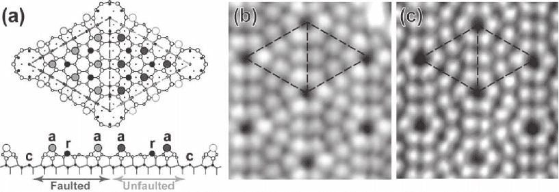
Figure 15–5. (a) Ball-and-stick model of the Si(111)–(7 × 7) surface. Top: top view; bottom: side view.
a, adatom; r, rest atom; c, corner hole. (b) Filled-state constant-current STM on Si(111)–(7 × 7); V = −1.0 V;
I = 0.4 nA. (c) Empty-state constant-current STM; V = +1.2 V; I = 0.4 nA.
978 P. Sutter
Rohrer, 1983) and electronic (Hamers et al., 1986) structure was solved
in pioneering STM experiments, and which continues to play an impor-
tant role in STM technique development. Figure 15–5a shows a struc-
ture model of the (7 × 7) reconstruction (Takayanagi et al., 1985). Figure
15–5b, obtained at negative sample bias (V = −1.0 V), i.e., with electrons
tunneling from occupied sample states to unoccupied tip states, shows
the corrugation associated with fi lled states of the sample. Conversely,
Figure 15–5c, obtained at positive sample bias (V = +1.2 V), maps the
empty states of the sample. Both images show atomic resolution, clearly
resolving the twelve adatoms (“a”) per unit cell. In addition character-
istic deep “corner holes” (“c”) bounding the diagonals of the 4.6 nm ×
2.9 nm rhombohedral unit cell are imaged.
While all adatoms are mapped uniformly in the empty state image,
the fi lled state scan shows one-half of the unit cell somewhat higher
than the other, an effect on the charge density due to the different
stacking sequence of atomic layers in the two halves of the unit cell. A
comparison of the images obtained at opposite bias polarity suggests
that in addition to surface topography, the electronic structure of the
sample surface adds substantially to the contrast observed in STM
imaging. This is implicit also in Eq. (1) via the dependence of the tun-
neling current on the local densities of states of both tip and sample at
the tunneling contact. Note also that the rest atoms (“r”), a second
near-surface species with dangling bonds protruding into the vacuum,
are imaged neither at positive nor at negative sample bias. A detailed
discussion of bias-dependent imaging and other tunneling spectro-
scopy methods used to assess the local electronic structure of a sample
surface is given in Section 3.
Apart from the structure of clean Si surfaces, Si-based surface chem-
istry has been studied widely by STM. Initial studies provided a knowl-
edge base for technological processes, such as reactive ion etching,
doping, and chemical vapor deposition (CVD). STM was used to probe
interactions of Si with halogens (Boland, 1993) and with small mole-
cules involved in surface passivation (H
2
, H; Laracuente and Whitman,
2001), doping (PH
3
; Wang et al., 1994a), and CVD growth (Si
2
H
6
; Wang
et al., 1994b). More recent research directions include the integration
of molecular electronic elements with Si. Under this perspective, the
covalent bonding of a wide variety of organic molecules on Si has been
studied (for a review, see Wolkow, 1999), including small molecules
such as ethylene (Mayne et al., 1993) and acetylene (Li et al., 1997),
simple alkenes (e.g., propylene; Lopinski et al., 1998) and polyenes (e.g.,
1,3-cyclohexadiene; Hovis and Hamers, 1997), pentacene (Kasaya et al,
1998), and benzene (Borovski et al., 1998). On clean Si(001), adsorption
is from the gas phase in UHV. H-passivated Si can also be modifi ed by
ex situ wet-chemical techniques, and reintroduced into UHV for STM
imaging.
Traditionally, an important aspect of the surface science of semicon-
ductors has been epitaxial growth. STM observations at initial growth
stages, i.e., at coverages of fractions of a monolayer (ML) up to several
ML, can provide direct insight into fundamental processes such as
adatom diffusion, incorporation into steps, and nucleation of mono-
Chapter 15 Scanning Tunneling Microscopy in Surface Science 979
layer islands (for a review, see Zhang and Lagally, 1998). Observations
of growth and equilibrium structures allow identifying kinetic and
thermodynamic factors affecting the growth process, as well as the role
of defects, of elastic strain, etc.
STM studies of Si epitaxy are commonly performed in either of two
modes. Conceptually preferred is the dynamic observation, via time-
lapse STM “movies,” of the growth surface with the sample held in the
microscope at high temperature and in the presence of a deposition
fl ux. This diffi cult technique will be discussed in more detail in Section
4. As an alternative, STM imaging can be performed at room tempera-
ture on samples that have been quenched at key stages in the growth
process. If measures are taken to verify that the quenched-in morphol-
ogy is indeed representative of that at high temperature during growth,
this “quench-and-look” technique offers the advantage of higher spatial
resolution and larger scan sizes over high-temperature STM.
Early STM experiments focused on the initial stages of Si homoepi-
taxy and Ge/Si heteroepitaxy, mostly on the technologically important
(111) or (001) surfaces. Key results include the identifi cation of regimes
of step-fl ow growth and nucleation, determination of the activation
energy and atomistic pathway of surface diffusion (Mo et al., 1991),
explanation of growth and equilibrium shapes of two-dimensional
(2D) islands (Mo et al., 1989), and exploration of the modifi cation of the
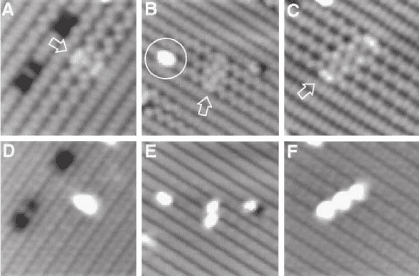
growth process by surfactants (Horn-von Hoegen, 1994). Figure 15–6
illustrates the identifi cation of the initial stage of island formation in
Figure 15–6. STM images of 0.01 monolayers Ge on Si(001). The long diagonal
bands are substrate dimer rows. Filled-state images (A–C; V = −2 V; I = 0.2 nA)
and corresponding empty-state images (D–F; V = +2 V; I = 0.2 nA), showing
rows of symmetric (bean-shaped) and asymmetric (buckled) substrate dimers,
and Ge adatom-induced chain-like structures (marked by arrows). The chain-
like paired adatom structures are seen as metastable precursors to the forma-
tion of monolayer islands in Ge/Si homoepitaxy (Reprinted with permission
from Qin and Lagally, © 1997 AAAS).
