Hawkes P.W., Spence J.C.H. (Eds.) Science of Microscopy. V.1 and 2
Подождите немного. Документ загружается.

1µm
0.001
0.2
0.1
0.01
32
-32
1/∆x [µm
-1
]
0.001
0.2
0.1
0.01
0.001
0.2
0.1
0.01
0.001
0.2
0.1
0.01
0 a.u. 1
a)
b)
c)
d)
0.001
0.2
0.1
0.01
32
-32
1/∆x [µm
-1
]
a)
b)
c)
d)
e)
I [MW/cm
2
]
0
1
0.2
0.75
0.25
0
F/F
0
f)
g)
h)
i)
0
1
0
0.3
0
0.3
800
200
b) [84 MW/cm
2
]
c) [187 MW/cm
2
]
d) [290 MW/cm
2
]
0.001 0.2
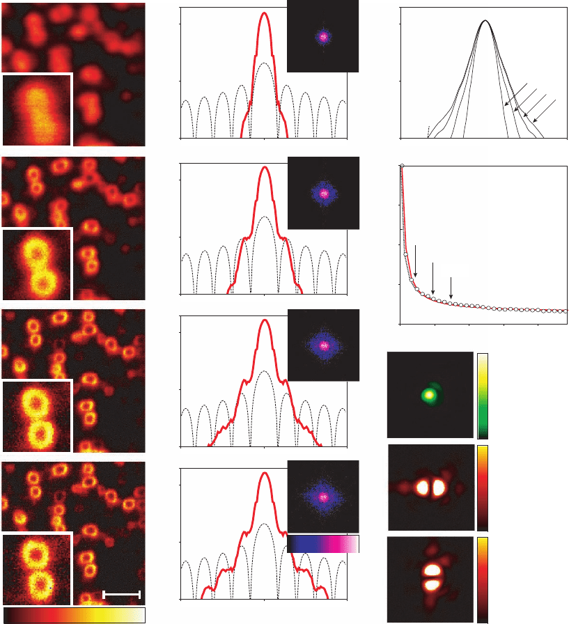
Figure 12–10. Images of a wetted Al
2
O
3
matrix featuring z-oriented holes (Whatman plc, Brentford,
UK) with a spin cast of a dyed (JA 26) polymethyl methacrylate solution. The rings formed in this way
are ∼250 nm in diameter and are barely resolved in confocal mode. (a–d) The confocal image (a) and
STED images with two depleting beams perpendicularly polarized and aberrated by “1D” phase-plates
(b–d). The excitation PSF (g) and the STED PSF for y polarization (h) and x polarization (i) are shown
on the right. The STED intensity was chosen at the spots marked in the saturation curve (f). The smaller
effective spot size also results in an extended OTF as seen in the second column. Here, the insets show
the 2D Fourier transformation of the images in the left and the graphs show a profi le along the x direc-
tion. Note the logarithmic scales. The Fourier transform of the image is given by the product of OTF
and the Fourier transform of the object [Eq. (2)]. For such regular structures, an estimate for the
modulus of the OTF can therefore be gained by estimating the latter and solving for the OTF. The
dashed line shows the Fourier transform of a ring with a diameter of 275 nm and a width of 50 nm and
the estimated OTF is presented in (e). (f) The suppression of fl uorescence resulting from stimulated
emission. The phase-plates were removed and the ratio of fl uorescence without STED light (F
0
) and
with the STED beams switched on (F) was recorded. The intensities are pulse intensities per beam at
the global maximum.
Plane
mirror
Bending
Magnet
Condenser
zone plate
Objective
zone plate
Pinhole
X-ray
sensitive
CCD
Sample
stage
National Synchrotron Light Source
X-ray Ring
X1 undulator
Monochromator
Zone plate
Order sorting
aperture
Detector
Specimen
So
ft x
ray
s
2.8 GeV electrons
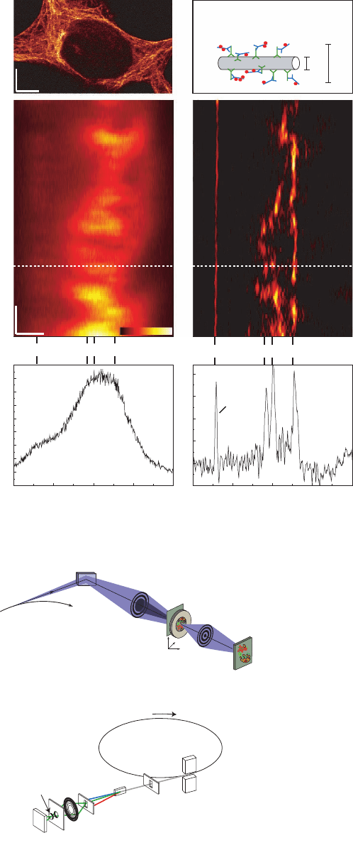
Figure 13–15. Schematic of the main components of
a transmission X-ray microscope or TXM (top: cour-
tesy of D. Attwood, Lawrence Berkeley National Lab-
oratory) and a scanning transmission X-ray microscope
or STXM (bottom: courtesy of Y. Wang, then of Stony
Brook.)
0
400
800
1200
1600
01234
Z / µm
Counts
Z / µm
FWHM
53nm
01234
1
2
3
z
x
Confocal
c)
e)
STED-4Pi
d)
f)
b)
25nm
60nm
Immunolabeled
microtubule
Overview
a)
Y
X
Monolayer
Microtubules
Monolayer
Microtubules
Figure 12–11. Subdiffraction immu-
nofl uorescence imaging with STED-4Pi
microscopy. (a) Overview image (xy) of
the microtubular network of an HEK
cell. (b) Sketch of typical dimensions of
a labeled microtubule fl uorescently
decorated via a secondary antibody. (c)
and (d) Standard confocal and STED-
4Pi xz image recorded at the same site
of the cell; the straight line close to the
cell stems from a monomolecular fl uo-
rescent layer attached to the adjacent
coverslip. In both images, the pixel size
was 95 × 9.8 nm in the x and z direction,
respectively; the dwell time per pixel
was 2 ms. Note the fundamentally
improved clarity in (d). The STED-4Pi
microscope’s PSF features two low side
lobes caused by the secondary minima
STED intensity distribution. These
lobes are <25% and were removed in
the STED-4Pi image using linear fi lter-
ing as outlined in the text [see Eq.
(16ff)]. (e) and (f) Corresponding pro-
fi les of the image data along the dashed
lines in (b) and (c) quantify the
improved axial resolution of the STED-
4Pi microscopy mode (f) over the con-
focal benchmark. Peaks 1, 2, and 3 due
to microtubules are broader than the
response to the monolayer. Note the
ability of the STED-4Pi microscope to
distinguish adjacent features.
2 µm
Abs. coeff.
µ (µm
-1
)
0
0.5
Flagella
Flagella
Flagellar roots
Flagellar roots
and neuromotor
and neuromotor
Nuclear
Nuclear
membrane
membrane
Cell wall
Cell wall
Nucleolus
Nucleolus
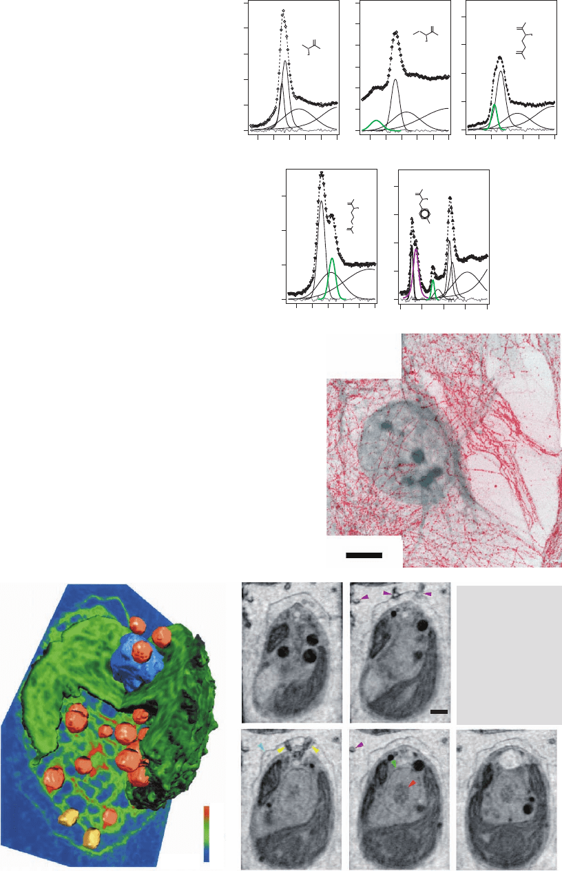
Figure 13–30. 3D rendering (left) and reconstruction slices (right) of the algae Chlamydomonas rein-
hardtii viewed by soft X-ray tomography at the BESSY I synchrotron. This alga was plunge-frozen in
liquid ethane, and imaged over 180º rotation sequence. The reconstruction is given in terms of the
quantitative linear absorption coeffi cient for 517 eV X-rays. (Reprinted from Wei et al., © 2000, with
permission from Elsevier.)
Figure 13–27. Near-carbon-edge
absorption spectra of several amino
acids, showing the effects of various
molecular bonds in the absorption
spectrum. These resonances can
be used for chemical contrast in X-
ray microscopy. (Reprinted from
Kaznacheyev et al., © 2002, with per-
mission from American Chemical
Society.)
OH
NH
3
+
O
O
OH
NH
3
+
O
NH
2
NH
OH
NH
3
+
O
OH
O
OH
NH
3
+
O
OH
NH
3
+
Arginine:
C=N
π*
Alanine:
aliphatic
Cysteine: side chain -SH
Glutamine: -NH2
Tyrosine: aromatic
292291290289288287
Photon Energy (eV)
292291290289288287 292290288286284
Mass Absorption Coefficient (10
4
cm
2
/g)
8
6
4
2
0
6
4
2
0
8
6
4
2
0
292291290289288287 292291290289288287
8
6
4
2
0
10
6
5
4
3
2
1
0
HS
6
+H
2
N
NH
2
3
Figure 13–29. Human fi broblast with immunogold
labeling for tubulin. This is a composite of two
images: a bright fi eld image (gray tones) to image
overall mass, and a dark fi eld image (red tones) to
selectively imaging the silver-enhanced gold labels.
This whole-mount cell was fi xed and then permeabo-
lized to allow for introduction of the immunogold
labels, after which it was air dried. (From Chapman
et al., © 1996b,c, courtesy of the Microscopy Society
of America.)
light epi
Si
Ca Mn
Fe
Ni
PS
Cu
K
Zn
10 µm
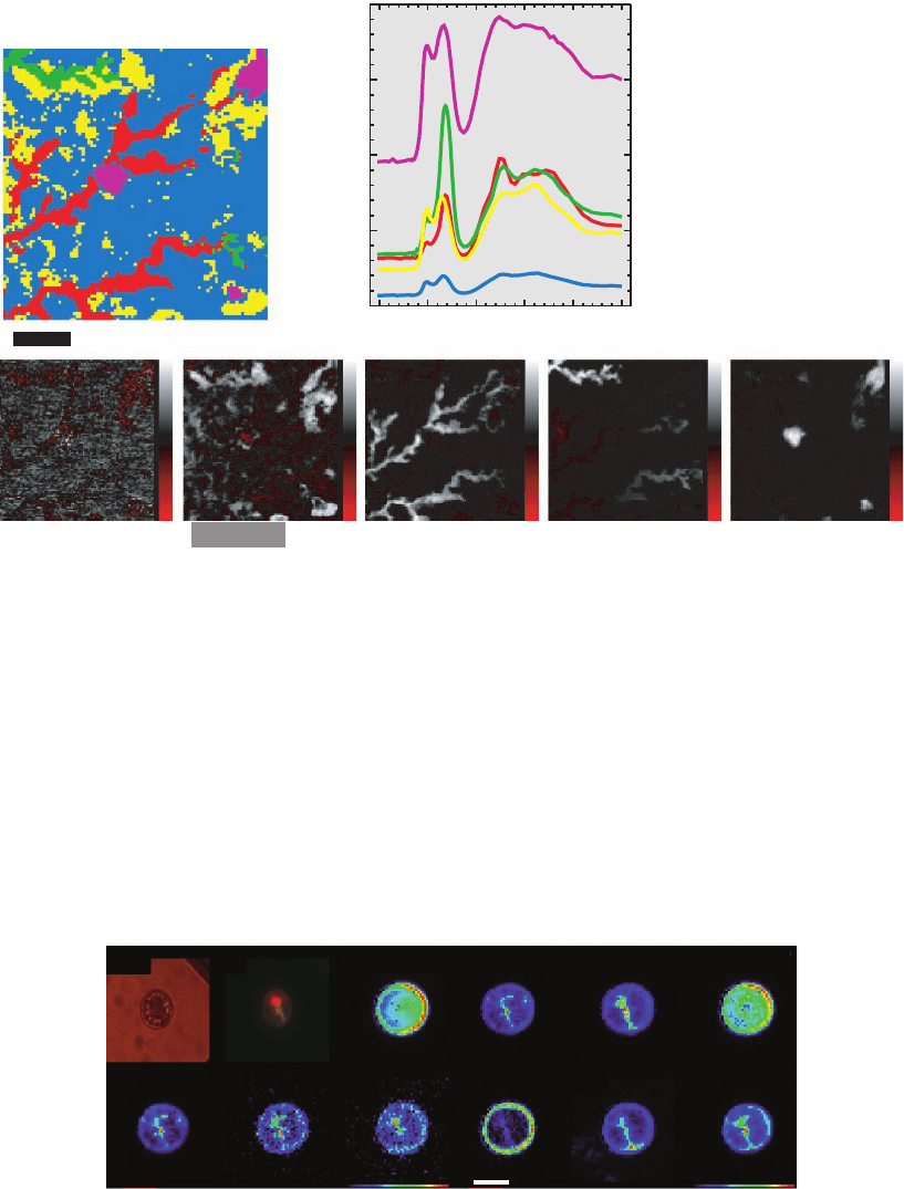
Figure 13–35. Visible light and epifl uorescence micrographs, and false color X-ray fl uorescence
element maps of a centric diatom collected from the southern Pacifi c. In this region of the ocean, iron
availability is a biolimiter with an impact on oceanic uptake of carbon dioxide from the atmosphere.
X-ray microprobes allow one to study iron content on a protist-specifi c basis. (Reprinted from Twining
et al., © 2003, with permission from American Chemical Society.)
Cluster 1 Cluster 2 Cluster 3 Cluster 4 Cluster 5
525 530 535 540 545 550
Photon energy (eV)
2 µm
0.0
0.5
1.0
1.5
2.0
Optical Density
Figure 13–34. Cluster analysis in a spectromicroscopy study of lutetium in hematite. Lutetium is
serving as a homologue to americium in an investigation of the uptake and transport of nuclear waste
products in groundwater colloids. By using a pattern recognition algorithm to search for pixels with
spectroscopic similarities, a set of signature spectra is automatically recovered from the data (shown
here in a color-coded classifi cation map) and thickness maps can be formed based on these signature
spectra. Analysis at the oxygen edge reveals two different phases of reactivity for lutetium with hema-
tite. Analysis by Lerotic (2004), from a study by T. Schäfer, INE Karlsruhe.

Intensity (a.u)
166 165 164 163 162 161 160
Binding Energy (eV)
S 2p
MoS
2
tips
sidewalls
base
Figure 13–42. In Electron Spectroscopy for Chemical Analysis or ESCA microscopy, a monochromatic
beam is used to illuminate a region several micrometers across; electron optics are then used to image
a tunable electron ejection energy to reveal surface chemistry. Though this does not involve zone plate
imaging, we include it here due to its widespread use with tunable X rays. In this case a 90-nm resolu-
tion ESCA microscope was used to locate aligned MoS
2
nanotube bundles and select certain areas
along the axes of the tubes for detailed examination. The image at left was acquired using Mo 3d
electrons, while S 2p, Mo 3d, and valence band spectra taken at the tips and sidewalls and the growth
base from the Si wafer appear strongly affected by the low dimensionality of the nanotubes and
differ signifi cantly from the corresponding spectra taken on a reference MoS
2
crystal. (Reprinted from
Kiskinova et al., © 2003, with permission of EDP Sciences.)
Figure 14–13. Transport imaging
in polycrystalline ZnO. (a) Surface
topography. (b and c) SSPM images
under lateral bias exhibit potential
drops at grain boundaries, indica-
tive of grain boundary resistive
behavior. Note that the direction of
potential drops inverts with bias.
(d) Current maps for positive and
negative bias polarity. (Partially
reproduced from Kalinin and
Bonnell, Zeitschrift fur Metallkunde,
90, 983–989, 1999.)
Figure 13–43. Scanning photoemission microscope (SPEM) study of a plasma display cell. In this micro-
scope the specimen is scanned through the zone plate focus while photoelectrons are collected by an electron
spectrometer. This fi gure shows a SPEM image, a scanning electron micrograph, and photoelectron spectra
from several regions of the sample. In a plasma display cell, light of the appropriate color emerges through a
front glass window which is protected from plasma damage by a composite insulating layer including MgO.
The photoelectron spectra show aging in the Mg(OH)
2
component of the layer over the life of the display cell.
(Reprinted from Yi et al., © 2005, with permission from the Institute of Pure and Applied Physics.)
SEM Image
SPEM image
Relative B.E. (eV) Relative B.E. (eV)
Degree of ageing
2
1
3
Relative B.E. (eV)
MgCO
3
MgO
Mg 2p, 2
MgCO
3
MgO
Mg(OH)
2
Mg 2p,1
Intensity (a.u.)
MgCO
3
MgO
Mg 2p, 3
5 0 -5 5 0 -5 5 0 -5
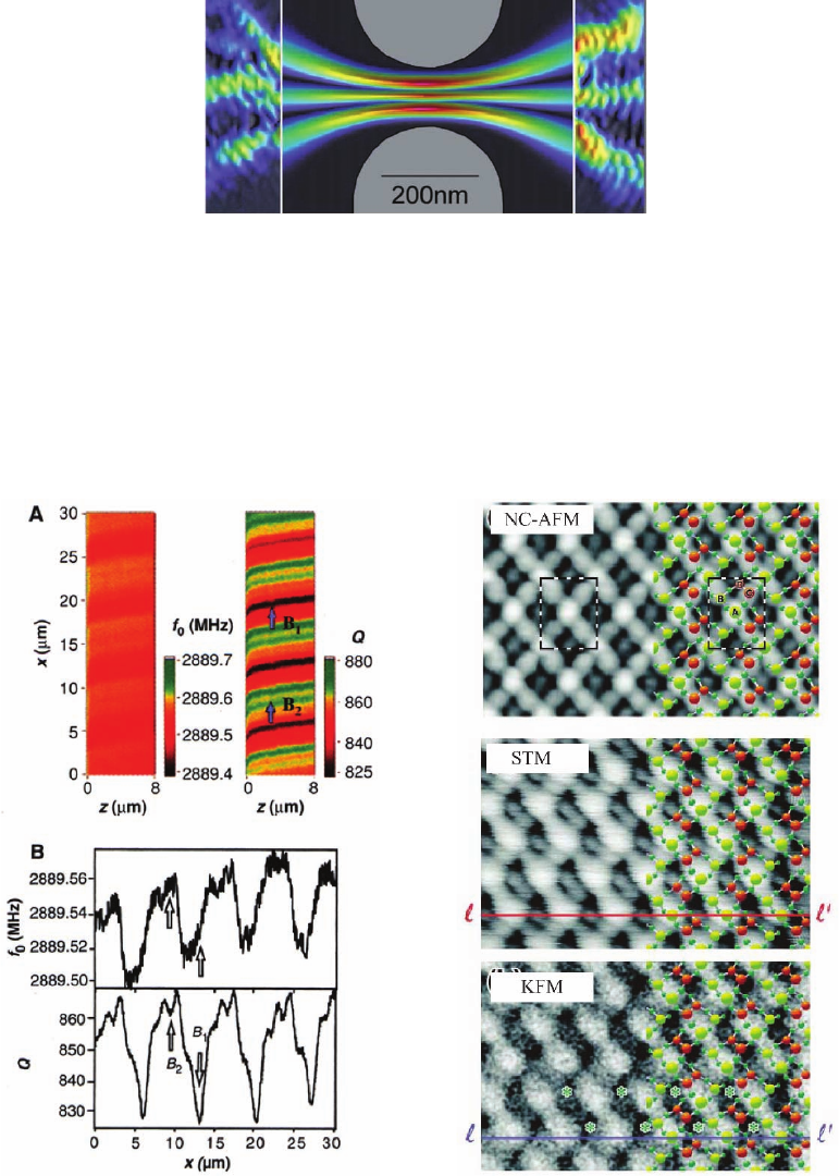
Figure 14–22. (A) Images of the profi les of peri-
odic dielectric constant (on the left) and ferro-
electric domain boundaries (on the right). (B)
Line profi les of frequency (top) and quality
factor (bottom) images.
Figure 14–23. Atomic resolution NC-AFM, STM,
and KFM on Ge/Si (105). [Courtesy of Eguchi et al.
Reproduced with permission from Physical Review
Letters, 93(26), 2004.]
Figure 14–15. Experimental images (outside) and theoretical simulations (inside) of the fl ow of elec-
tron waves through a quantum point contact. Fringes spaced by half the Fermi wavelength demon-
strate coherence in the fl ow. [Courtesy of Westervelt et al. Reproduced with permission from Physica
E, 24, 63–69, 2004.]
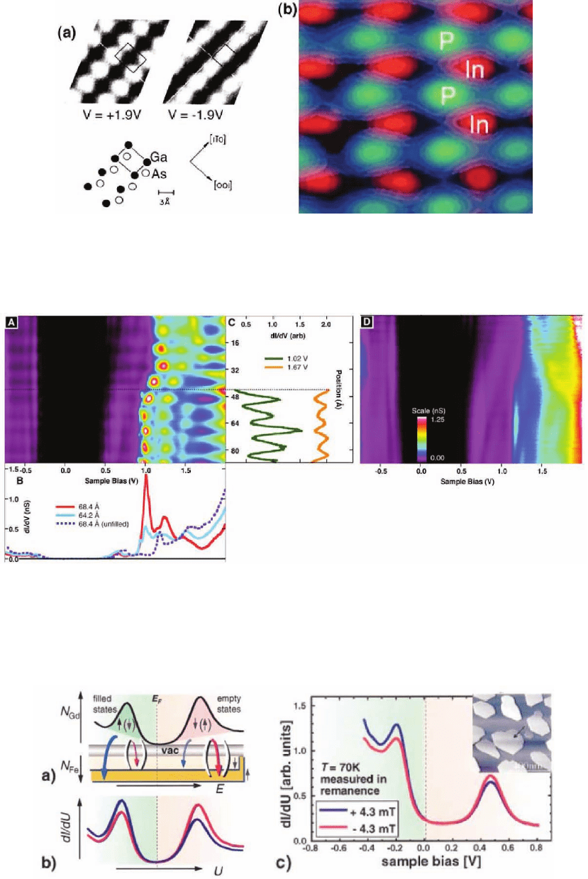
Figure 15–13. (a) Bias-dependent STM on GaAs(110): selective imaging of Ga and As sublattices at
positive and negative sample bias, respectively (Reprinted with Permission from Feenstra et al., ©1987
by the Armeucion Physics Socuity). (b) Compound STM image of the InP(110) surface, assembled from
separate positive and negative bias scans (Reprinted from Ebert et al., ©1992 with permission from
Elsevier).
Figure 15–16. I(V) tunneling spectroscopy on C
60
/C-nanotube “peapods” (Reprinted with Permission
from Hornbaker et al., ©2002 AAAS). (A) Map of an array of full dI/dV spectra along the axis of a C-
nanotube “peapod.” Sample bias voltage is plotted on the horizontal axis and displacement along the
tube on the vertical axis. (B) Representative dI/dV spectra at selected positions along the tube. Large
conductance peaks are found at positions of embedded C
60
molecules. (C) Variation of tunneling con-
ductance along the tube axis. (D) Reference spectroscopic map on an empty C-nanotube section
without embedded C
60
, in which no strong modulation of the tunneling conductance is observed.
Figure 15–18. Spin-polarized STM on a Gd(0001) sample with an exchange-split surface state and a
magnetic Fe tip with constant spin polarization close to E
F
. (a) Due to the spin-valve effect the tun-
neling current of the surface state spin component parallel to the tip magnetization is enhanced. (b)
Illustration of the reversal in the dI/dV signal at the surface state peak position upon switching the
sample magnetically. (c) Experimental observation of this reversal in tunneling into an isolated Gd
island (Reprinted with permission from Bode et al., ©1998 by the American Physical Society).

Figure 16–1. STM topographies of Rec-DNA complex (left) and an aberrant bacteriophage capside
(right). In the upper right corner, a hole has been created applying a voltage pulse between the tip and
the sample. Both images immediately reveal the molecular arrangement of the respective complex
structure. (Left, from Amrein et al., 1988, reproduced with permission. Right, from Amrein et al., 1998b,
reproduced with permission.)
Figure 15–37. Identifi cation of
the molecular conformation of
Cu-DTBPP on Cu(211). (a) Molec-
ular model of Cu-DTBPP, with the
four-lobed pattern observed by
STM marked in yellow. (b–e) STM
contrast calculation for different
angles between the four legs and
the substrate: (b) 60°, (c) 45°, (d)
30°, and (e) 10°. (f) Experimental
STM image of the molecule.
(Reprinted from Moresco et al.,
©2002 with permission from
Elsevier.)
Figure 16–3. Neuronal cell, cultured on an electronic
chip. The chip is designed such as to pick up an action
potential of the cell. The image demonstrates proper
tracing of the cell surface. In a future application, an
appropriately designed stylus might be used as an
additional electrode to excite or record an action
potential at any location of the cell body or a process
of the neuronal cell.
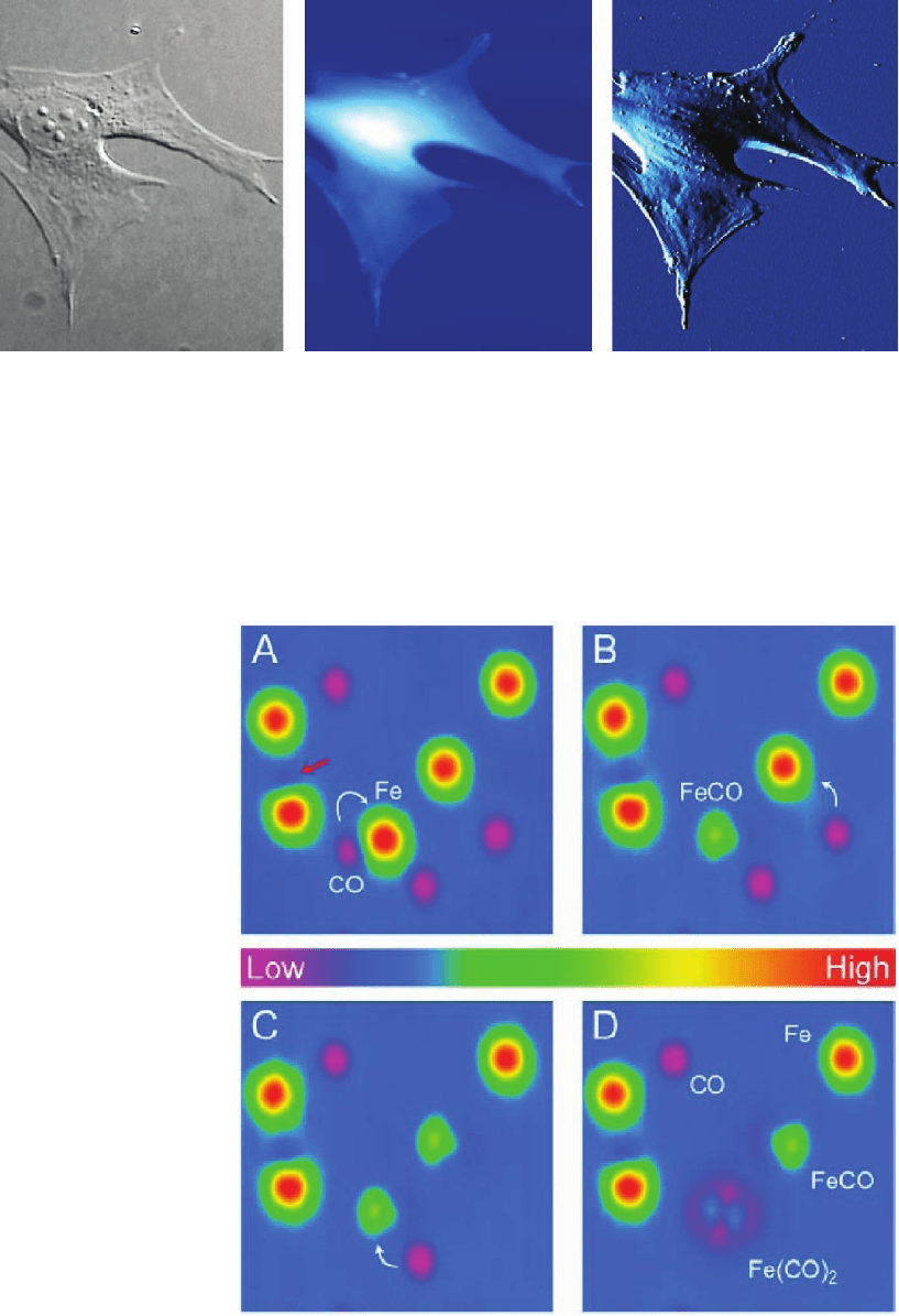
Figure 16–18. Images of a fi xed 3T3 cell in buffer, on a coverslip. Left to right: Optical (differential
interference contrast, DIC) and simultaneous AFM (JPK Instruments, contact mode) topography and
feedback signal.
Figure 17–36. Bond for-
mation induced with
STM tip. A sequence of
STM constant-current
images at 13 K showing
the formation of Fe–CO
bonds by vertical manip-
ulation. Fe atoms are
imaged as protrusions
and CO molecules as
depressions. The white
arrows indicate the pair
of adsorbates involved
in each bond formation
step. In (B) and (C) a CO
molecule has been
picked up and bonded
to an Fe atom to form
Fe(CO). In (D) a second
CO molecule has been
bonded to Fe(CO) to
form Fe(CO)
2
. (From Lee
and Ho, 1999.)
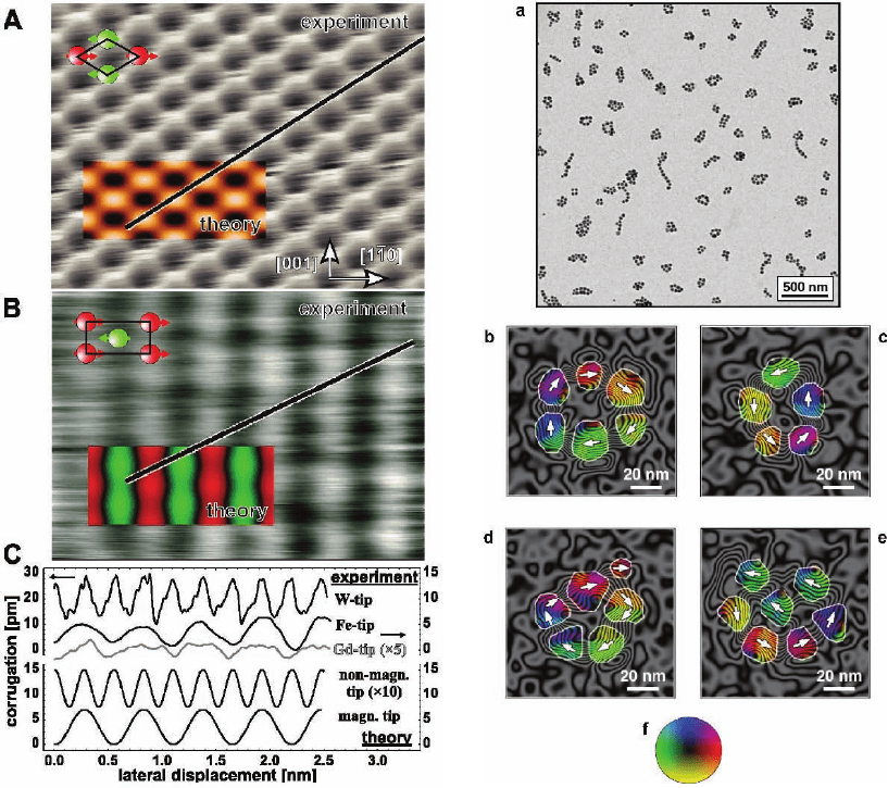
Figure 17–43. Atomic resolution magnetic imagi ng
with SP-STM. (A) Constant-current image of one
monolayer of Mn on W(110) recorded with a non-
magnetic W tip at 16 K. (B) Image recorded with a
magnetic Fe tip showing an antiferromagnetic con-
fi guration as predicted by theory. The colored
insets show calculated STM images. (C) Experi-
mental and theoretical line sections from (A) and
(B). The image size is 2.7 nm by 2.2 nm. (From
Heinze et al., 2000.)
Figure 18–9. (a) Low magnifi cation bright-
fi eld image of self-assembled Co nano-
particle rings and chains deposited onto an
amorphous carbon support fi lm. Each Co par-
ticle has a diameter of between 20 and 30 nm.
(b–e) Magnetic phase contours (128× amplifi -
cation; 0.049 radian spacing), formed from the
magnetic contribution to the measured phase
shift, in four different nano particle rings. The
outlines of the nano particles are marked in
white, while the direction of the measured
magnetic induction is indicated both using
arrows and according to the color wheel shown
in (f) (red = right, yellow = down, green = left,
blue = up). (Reprinted from Dunin-Borkowski
et al., 2004b.)
