Hawkes P.W., Spence J.C.H. (Eds.) Science of Microscopy. V.1 and 2
Подождите немного. Документ загружается.

980 P. Sutter
Ge/Si(001) epitaxy (Qin and Lagally, 1997). Classic theories of nucle-
ation in thin fi lm growth are based on the notion of a “critical nucleus,”
defi ned as the structural entity for which the addition of one more atom
will for the fi rst time reduce the free energy. Employing very low Ge
coverages and high-resolution dual bias STM imaging to uncover the
link between monomer adsorption and initial 2D growth islands, this
study shows that island formation may not involve a “critical nucleus,”
but instead may proceed via a family of metastable structures of
varying size, with signifi cant consequences on many growth models
that are based on nucleation and require the size of a critical nucleus
as input.
More recently, interest has concentrated on strained layer heteroepi-
taxial growth, e.g., of Si
1−x
Ge
x
alloys on Si(001), as an elegant way of
producing large arrays of nanostructures. Si and Ge are miscible over
the entire composition range, and the lattice mismatch in the Si
1−x
Ge
x
/
Si(001) system can be tuned between 0 and 4% by alloying. Over a wide
range of compositions, Si
1−x
Ge
x
alloys initially wet the Si substrate, and
at higher coverage develop coherent (i.e., dislocation free) faceted three-
dimensional (3D) islands that lower the free energy by relaxing part
of the lattice mismatch strain. Potentially useful in electronics or opto-
electronics, these faceted nanostructures have shown a strikingly
complex array of growth phenomena, which make them interesting for
fundamental growth studies.
Constant current STM images with atomic resolution typically
encompass fi elds of view of few tens of nanometers. Combining a drift-
stable microscope with state-of-the-art control electronics, substantially
larger atom-resolved images have become feasible. The ability to obtain
image sizes in excess of 1 µm
2
with high resolution is potentially pow-
erful for imaging growth processes, since it provides access to all rele-
vant length scales as well as image statistics far superior to that of
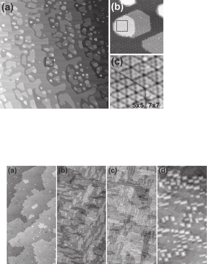
conventional small scans. Figure 15–7 illustrates this capability with
an STM image of 1.5 monolayers Ge on Si(111) with a fi eld of view of
0.75 µm and 0.05 nm pixel size. The large scan provides an excellent
overview of the step and island structures resulting from monolayer
Ge deposition. At progressive zoom into the image, individual terraces,
and, ultimately, single surface defects and reconstruction domains
(here coexisting 7 × 7 and 5 × 5 domains) can be examined.
Figure 15–8 gives an example in which the superior statistics result-
ing from large atom-resolved images was used successfully to pinpoint
the mechanism of periodic surface roughening in Ge/Si(001) growth
(Sutter et al., 2003a). Via a sequence of “quench-and-look” experiments
at different Ge coverages, short-range interactions between surface
steps and vacancy lines, periodic arrays of linear chains of dimer
vacancies, are shown to cause a highly correlated surface roughness in
the form of anisotropic 2D islands with progressively higher aspect
ratio (a–c). Finally, images obtained at a critical Ge coverage of four
atomic layers (d) show the transition from 2D to 3D growth by forma-
tion of the fi rst faceted islands on the rough wetting layer, and identify
the atomic-scale pathway of the 2D–3D transition.
Chapter 15 Scanning Tunneling Microscopy in Surface Science 981
Figure 15–7. Large-area atom-resolved STM. (a) STM image with 0.75-µm
fi eld of view and 0.05-nm pixel size, showing the surface morphology of Si(111)
after deposition of 1.5 ML Ge at 550°C. An array of parallel steps, running
diagonally from the upper left to lower right, coexists with islands nucleated
during Ge deposition. (b) Zoomed-in view (50 nm) of the area marked by a
square in (a), showing one of the islands. (c) Further zoom-in (10 nm), showing
the coexistence of (7 × 7) and (5 × 5) reconstructed domains in the area marked
in (b).
Figure 15–8. Transition from 2D to 3D morphology in the growth of Ge on Si(001). Large-area atom-
resolved STM images (250 nm × 125 nm sections are shown here) illustrate the surface morphology at
(a) 1.5 ML, (b) 2.3 ML, (c) 3.5 ML, and (d) 4.0 ML Ge coverage. The transition to 3D growth is preceded
by the formation of highly correlated, anisotropic surface roughness. With the superior statistics of
large-area high-resolution images, the repulsive interaction between surface steps and defects (dimer
vacancy lines) was identifi ed as the origin of the ordering of this surface roughness. (Reprinted with
permission from Sutter et al., © 2003a by the American Physical Society.)

982 P. Sutter
Initial 3D islands with shallow facets, such as those shown in Figure
15–8d, evolve into more complex shapes involving steeper facets, which
give rise to more effi cient strain relaxation (Figure 15–9). For Si
1−x
Ge
x
epitaxy on Si(001), the facets bounding the islands identifi ed by STM
are to a large extent major stable facets of Si and Ge (Figure 15–9a). At
early stages of 3D growth, shallow (105) faceted “huts” are invariably
observed (Figure 15–9b; Mo et al., 1990). These islands then undergo a
shape transformation to become multifaceted “domes” (Figure 15–9c;
Medeiros-Ribeiro et al., 1998). At later stages in the shape evolution,
elastic strain relaxation increasingly competes with plastic relaxation
via dislocations. For Ge/Si(001) dislocations are introduced before the
“dome” shape can transform further by introducing additional steeper
facets. By reducing the Ge concentration of Si
1−x
Ge
x
alloys, and thus
lowering the lattice mismatch strain, the coherent shape evolution has
been extended beyond the “dome” shape to the end-point in the
stereographic triangle, where steep (111) facets are introduced (Sutter
et al., 2004).
3 Tunneling Spectroscopy
Equation (1) gives an expression for the tunneling current I in the WKB
approximation for planar tunneling. In this approximation the tunnel-
ing current is an integral, over the energy range of width |eV| in which
tunneling can occur, of a product of the densities of states (DOS) of tip
[ρ
T
(E)] and sample [ρ
S
(E)] multiplied by the transmission probability,
T(E, eV). While this simple approximation cannot address the high
spatial resolution of STM—a more elaborate theory capable of address-
ing this aspect will be discussed in Section 6—it demonstrates that the
tunneling current is affected by the electronic structure of both the tip
and the sample. In a large number of applications it would be desirable
to merely map the atomic scale “topography” of a sample. The sensitiv-
ity of the tunneling current to the DOS can then be a disadvantage,
since it often prevents a simple interpretation of a tunneling image as
Figure 15–9. Shapes of coherent (i.e., dislocation-free) 3D islands induced by lattice mismatch strain
during Si
1−x
Ge
x
/Si(001) heteroepitaxy. (a) Unit stereographic triangle for Si, showing the major and
minor stable facets (Gai et al., 1998). (b) STM top view, showing a shallow (105) faceted “hut.” (c) Mul-
tifaceted “dome” shape, terminated by (105), (113), and (15 3 23) facets. (d) “Barn”-shaped 3D island,
observed for low-misfi t Si
1−x
Ge
x
alloys on Si(001), transformed from a “dome” by introduction of addi-
tional (111) facets (Reprinted with permission from Sutter et al., © 2004 American Institute of
Physics.).
Chapter 15 Scanning Tunneling Microscopy in Surface Science 983
a “topographic” map. For many metals with small variations in the
DOS near the Fermi energy such a simple interpretation is often pos-
sible, i.e., height maxima in a constant current STM image are corre-
lated with atomic positions. However, for semiconductors with strongly
varying DOS near E
F
, the simple picture frequently breaks down.
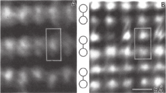
An example is the (001) surface of Si. Geometrically, this surface
consists of Si dimers, in which each atom is bonded to two atoms in
the second layer and to its dimer partner. Constant-current STM images
obtained on Si(001) at positive sample bias indeed show two maxima
in each dimer (Figure 15–10B), which could be interpreted as the
“atomic positions.” At negative sample bias, however, only a single
broader bean-shaped structure is observed (Figure 15–10A), which
extends across each dimer. In fact, the tunneling current in empty-state
STM (positive sample bias) refl ects the charge distribution in a π* anti-
bonding state just above the Fermi energy, whose wave function has a
node at the center of the dimer. Even in this case in which the STM
image shows two maxima per dimer, these maxima do not refl ect the
atomic positions in the dimer. Worse yet, in fi lled-state STM (negative
sample bias) a π bonding state is imaged whose charge density peaks
at the center of the dimer bond, thus giving rise to a single “topo-
graphic” maximum at that position.
The sensitivity to the electronic structure of tip and sample, however,
is not merely a complication in STM imaging. It is also one of the major
strengths of the technique, since it allows measuring and mapping
surface electronic structure with very high spatial resolution well
below 1 nm. While most other techniques, such as ultraviolet or x-ray
photoelectron spectroscopy or Auger electron spectroscopy, average
over macroscopic sample areas, recently developed spectromicroscopy
techniques, such as synchrotron photoelectron emission micro-
scopy, provide spectroscopic imaging with 10 nm spatial resolution (see
Chapter 8, this volume). However, measurements of surface electronic
Figure 15–10. Constant-current STM images of Si(001) at negative [V = −1.6 V
(A)] and positive [V = +1.6 V, (B)]. The (2 × 1) unit cell is outlined, and the loca-
tions of the dimers are shown in the center. (Reprinted with permission from
the Annual Review of Physical Chemistry, Volume 40 © 1989 by Annual
Reviews www.annualreviews.org.)
984 P. Sutter
structure “atom-by-atom,” summarized under the term scanning tun-
neling spectroscopy, are feasible only by STM.
3.1 Bias-Dependent Imaging
The simplest scenario for gathering electronic structure information
involves the successive measurement of constant-current STM images
at different sample bias. As discussed in Section 1, the tunneling trans-
mission probability is generally highest at the Fermi energy of the
negatively biased electrode, and falls off exponentially at lower ener-
gies. For positive sample bias, i.e., empty-state STM, elastic tunneling
occurs mainly from states near the tip Fermi energy into unoccupied
sample states. In this polarity, varying the bias voltage probes different
surface states of the sample, particularly if the electronic structure of
the tip varies slowly in the energy range defi ned by the bias voltages
used. A series of constant-current STM images at different bias can
thus be used to map the spatial distribution of unoccupied surface
states of the sample.
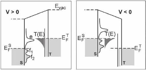
For negative voltages applied to the sample, i.e., fi lled-state STM, the
situation is not as fortunate. The tunneling current is now dominated
by states near the Fermi level of the sample. As a result, the occupied
sample state with highest energy is invariably imaged preferentially
(Becker et al., 1989). Even if lower-lying surface states exist, as indicated
schematically in Figure 15–11, constant-current STM imaging is rather
insensitive to those states.
As a possible solution to this problem in bias-dependent fi lled-state
imaging it has been suggested that metal probe tips with smoothly
varying density of states near the Fermi energy could be replaced by
a semiconductor tip with a strongly modulated DOS. Band structure
effects have long been recognized in the interaction of low-energy
electrons with metal surfaces (Bauer, 1994). As an example, the high
normal incidence refl ectivity on W(110) at low electron energies is due
to a (110) projected band gap extending over 5 eV, i.e., a lack of extended
bulk states in the energy range of this gap. For W(100), such a gap does
Figure 15–11. Band diagrams illustrating the bias-dependent tunneling
between tip (T) and sample (S). Sample bias V > 0: empty-state STM. V < 0:
fi lled-state STM. T(E) shows schematically the transmission probability as a
function of energy for states participating in the tunneling process.
Chapter 15 Scanning Tunneling Microscopy in Surface Science 985
not exist. Low-energy electrons can propagate into extended states, and
the refl ectivity in the same energy range is low. Similarly, it can be
expected that a lack of fi nal states due to projected band gaps in the
STM tip material can signifi cantly affect the tunneling probability in
the energy range spanned by such gaps. This modulation of the trans-
mission probability could be used for effi cient energy fi ltering of the
tunneling current in constant-current STM, specifi cally in fi lled-state
imaging.
Calculations by density functional theory (DFT) show a number of
gaps in the [111]-projected band structure of III–V compound semicon-
ductors such as InAs. III–V compound semiconductors cleave easily at
(110) planes, and cleavage corners bounded by {110} and (100) planes
are suffi ciently sharp for atomic-resolution STM (Nunes and Amer,
1993). In addition, InAs(110) has the advantage of an unpinned surface
with minimal band bending and slight electron accumulation. The
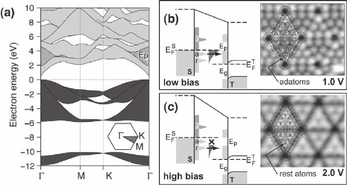
feasibility of energy-fi ltered STM has been demonstrated by using a
cleaved InAs tip to selectively image different occupied surface states
on Si(111)-(7 × 7) (Sutter et al., 2003b). In these experiments, summa-
rized in Figure 15–12, a [111]-projected gap in the InAs conduction
band, centered at Γ and about 2.6 eV wide, is used to modulate the
tunneling current in fi lled-state constant current STM. The “adatom”
state (“a”) on Si(111)-(7 × 7), which lies only 0.35 eV below the Fermi
energy and is imaged by STM using a metal tip, dominates the tunnel-
ing current at low tip–sample bias. At higher bias, this state aligns with
a projected gap in the InAs conduction bands and its tunneling
probability is reduced sharply. Under these conditions the “rest atom”
Figure 15–12. Energy-fi ltered STM. (a) Bulk band structure of monocrystalline InAs probe tips, pro-
jected along the (111) zone axis parallel to the tunneling direction. E
p
denotes a projected gap in the
bulk conduction band. (b) Band diagram and STM image for low-bias fi lled state STM with InAs tips,
demonstrating preferential imaging of the adatom state on Si(111)-(7 × 7). (c) High-bias fi lled state
InAs-tip STM on Si(111)-(7 × 7): alignment of the adatom state with the projected tip gap reduces its
contribution to the tunneling current, giving rise to preferential imaging of the energetically lower
rest-atom state (Reprinted with permission from Sutter et al., © 2003b by the American Physical
Society).
986 P. Sutter
state (“r”), a surface state 0.8 eV below E
F
that is not accessible in con-
ventional STM imaging, contributes a majority of the tunneling current
and can be imaged selectively. Importantly, these results suggest that
robust bulk band structure effects, which are independent of the atomic
structure of the tip, can be used to modulate the transmission probabil-
ity in vacuum tunneling. Once developed into a routine imaging tech-
nique, energy-fi ltered STM has the potential to provide rich spectroscopic
contrast within the relatively simple framework of bias-dependent
constant current STM.
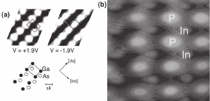
A classic example of a scenario in which conventional bias-
dependent imaging provides directly interpretable spectroscopic infor-
mation is imaging of cation and anion sites on (110) cleavage planes of
compound semiconductors such as GaAs (Feenstra et al., 1987) or InP
(Ebert et al., 1992) (Figure 15–13). For (110) surfaces of compound semi-
conductors, such as GaAs, the occupied state density (imaged at nega-
tive sample voltage) is localized on the anions (As, P), while the
unoccupied state density (positive sample voltage) is localized on
the cations (Ga, In). As a result, bias-dependent STM imaging can be used
to selectively image the cation and anion sublattices on these surfaces.
3.2 Local I-V Measurements and Current Imaging
Tunneling Spect roscopy
In many instances, a complete electronic structure map is not required,
but one would like to determine, at one or several positions on a
sample, the surface density of states in an interval of a few eV around
the Fermi energy. Such local measurements can, for example, serve
to determine if a specifi c surface reconstruction or a small cluster is
semiconducting or metallic, to measure the band gap at the surface
of semiconductor samples, and to determine for a given location the
energies of surface states.
Figure 15–13. (a) Bias-dependent STM on GaAs(110): selective imaging of Ga and As sublattices at
positive and negative sample bias, respectively (Reprinted with Permission from Feenstra et al., ©1987
by the Armeucion Physics Socuity). (b) Compound STM image of the InP(110) surface, assembled from
separate positive and negative bias scans (Reprinted from Ebert et al., ©1992 with permission from
Elsevier). (See color plate.)
Chapter 15 Scanning Tunneling Microscopy in Surface Science 987
Local current–voltage [I(V)] spectra serve this purpose. The basic
information content of a tunneling I(V) spectrum can be demonstrated
by differentiating Eq. (1) [V > 0]:
dI
dV
eeV TeVeV e E E eV T E
ss
=
(
)
(
)
(
)
+
(
)
−
(
)
∂ρρ ρρ
TT
0, ,,/
,
eV
deV e E E eVTEeV dE
eV
s
(
)
[
(
)
−
(
)
′
−
(
)
(
)
]
∫
0
ρρ
T
(4)
For a given energy eV, the tunneling conductance dI/dV refl ects the
density of states of the sample at that energy, ρ
S
(eV).
Feenstra et al. (1987) noted diffi culties with conductance spectros-
copy, resulting from the fact that the expression for dI/dV diverges
exponentially both in voltage (V) and separation (z). These divergences
can be eliminated by normalizing dI/dV by the conductance of the
tunneling junction, [dI/dV]/[I/V] ≈ d(lnI)/d(lnV). In this form, spe-
ctra obtained at different tip–sample separation z can be compared
directly.
Local spectroscopy is quite simple to perform. The STM tip is posi-
tioned and stabilized over a chosen point on the sample. The feedback
loop is switched off while the sample voltage is varied over the desired
values, and a local measurement of tunneling current as a function of
bias voltage, I(V), is performed. As an alternative, the tunneling con-
ductance, dI(V)/dV, can be measured by ramping the bias voltage with
a small ac voltage added, and measuring the ac component of the tun-
neling current at the modulation frequency of the ac part by lock-in
techniques. After the I(V) or dI(V)/dV spectrum is recorded, the tip
feedback is reactivated, and STM imaging can resume.
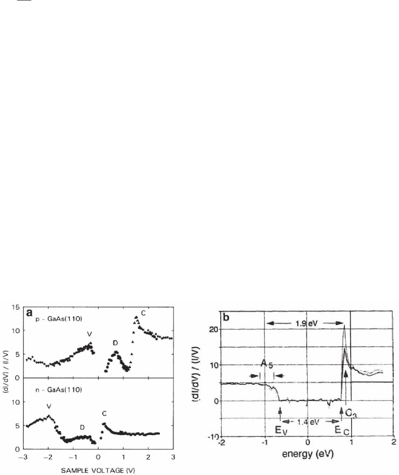
Figure 15–14a shows tunneling conductance spectra obtained on p-
and n-type GaAs(110) (Feenstra et al., 1987), which provide a measure
Figure 15–14. (a) Local normalized conductance spectra obtained on n- and p-doped GaAs(110),
showing three peaks (V, D, C) originating from surface states (Feenstra et al., 1987). (b) Normalized
conductance spectra obtained on InP(110), illustrating the valence and conduction band edges delimit-
ing the bulk bandgap (1.4 eV), and the A
5
and C
3
surface states defi ning the surface gap (1.9 eV)
(Reprinted from Ebert et al., © 1992 with permission from Elsevier).
988 P. Sutter
of the surface state density. The spectra show three distinct peaks
associated with surface states. Peak C is related to a state in the GaAs
conduction band, localized on the Ga atoms, while peak V stems from
a valence state localized on the As anions. Peak D is associated with
tunneling of dopant-induced carriers within the bulk band gap. The
separation between the leading edges of the C and V peaks is close to
the bulk band gap of GaAs (E
g
= 1.43 eV), i.e., in this system tunneling
spectroscopy can be used to determine the band gap. Figure 15–14b)
shows tunneling conductance spectra on the (110) cleavage surface of
another III–V compound, InP. Also for InP, the band gap (∼1.4 eV) is
evident from sharp onsets of signifi cant state density at the valence
and conduction band edges. However, for this system it was argued
that a wider surface band gap (∼1.9 eV) is indirect, delimited by a
surface state C
3
at the edge of the surface Brillouin zone and a broad-
ened state A5 at the zone center.
A natural, albeit experimentally much more complex extension of
local I(V) spectroscopy is the measurement of tunneling spectra, as
discussed above, at each image pixel of a constant-current STM scan.
This measuring scheme is called current-imaging tunneling spectro-
scopy (CITS). Since complete I(V) spectra are obtained at each image
point, the corresponding data sets can provide a full range of spectro-
scopic information. As an example, current maps I(x, y) at fi xed tip–
sample bias can be produced. Instead, the voltage dependent tunneling
conductance dI(V)/dV can be calculated numerically and mapped as a
function of sample position. If the chosen voltage corresponds to the
energy of a surface state of the sample, conductance maps will provide
a direct image of the spatial distribution of that state. Due to the com-
plexity of the data acquisition, the experimental requirements for CITS
are quite stringent. Since complete I(V) curves are measured at each
image pixel, requiring the stopping of a scan and deactivation of the
feedback loop for a fraction of a second per spectrum, a very high sta-
bility of the tunneling gap and low lateral drift of the tip relative to
the sample are of key importance. These conditions are more easily
fulfi lled at cryogenic temperatures, where a z-stability of the order of
1 pm and lateral drift velocities of the order of few Å/hour are possible.
Low temperatures also reduce the thermal broadening of the tunneling
transmission coeffi cient T(E), and thus narrow the linewidth of fea-
tures in the tunneling spectra.
A classic example of the application of CITS, the measurement of the
electronic structure of Si(111)-(7 × 7), is shown in Figure 15–15 (Hamers
et al., 1986). Shown are a constant current image of the surface at +2 V
sample bias (a), as well as current images acquired during the same
scan at bias voltages of +1.45 V and −1.45 V, showing spatial maps of
unoccupied (+)/occupied (−) sample states at energies up to 1.45 eV
above/below the Fermi energy. CITS difference images, a precursor to
modern dI/dV maps, discussed below, calculated by numerically sub-
tracting current images at energies bracketing those of specifi c surface
states, allowed the mapping of the adatom state, dangling bond, and
backbond state on this complex reconstructed surface.

Chapter 15 Scanning Tunneling Microscopy in Surface Science 989
More recently, this complex data acquisition mode has been used,
for example, to map modifi cations in the electronic structure of indi-
vidual carbon nanotubes arising with the supramolecular assembly of
C
60
molecules inside the hollow tube to form nanotube “peapods”
(Hornbaker et al., 2002). dI/dV spectra obtained along the symmetry
axis of C nanotubes show distinct peaks in the density of unoccupied
states with a spatial periodicity corresponding to the average spacing
of embedded C
60
molecules observed by transmission electron micros-
copy, suggesting that the insertion of C
60
causes a signifi cant modula-
tion of the electronic structure. A control measurement was constructed
by using the STM tip to push the C
60
away, and remeasuring dI/dV
spectra along the same nanotube section without embedded C
60
. The
empty tube obtained in this way shows small and smooth variations
in the density of states along the nanotube axis. Qualitatively, the elec-
tronic structure of the peapods was explained by the single wall C-
nanotube acting as a conduit that enhances the coupling between C
60
molecules nested inside it, and the Bragg scattering of nanotube states
due to the periodic arrangement of the C
60
. Calculations of the peapod
electronic structure confi rm the formation of a hybrid electronic band,
which derives its character from both the nanotube states and the C
60
molecular orbitals (Figure 15–16).
3.3 Differential Conductance (dI/dV) Mapping
For a given energy eV, the tunneling conductance dI/dV refl ects the
density of states of the sample at that energy, ρ
S
(eV). As a result, it can
be expected that high-resolution maps of tunneling conductance can
provide detailed information on spatial variations in sample electronic
structure. For example, by plotting dI/dV at an energy corresponding
to a localized state at the sample surface, the spatial distribution of that
sample state can be mapped.
In a typical experiment a constant current image, at a specifi c bias
voltage and tunneling current used to stabilize the tunneling gap, is
Figure 15–15. Current-imaging tunneling spectroscopy on Si(111)-(7 × 7) (Hames et al., 1986). (a)
Constant-current STM image (V = +2 V), with one (7 × 7) unit cell outlined (F, faulted; U, unfaulted
half). (b and c) Current images obtained at +1.45 V and −1.45 V, respectively. Note the strong similarity
between the rest-atom contrast in the current image (c), and the contrast obtained in rest-atom imaging
by energy-fi ltered constant-current STM (Figure 15–12).
