Hawkes P.W., Spence J.C.H. (Eds.) Science of Microscopy. V.1 and 2
Подождите немного. Документ загружается.

1010 P. Sutter
measured Schottky barrier height were detected, emphasizing the
need for high-resolution maps of interfacial transport.
Carrier transport in BEEM is affected by all stages of the injection
pathway: (1) tunneling from the tip into the metal base layer, (2) hot
carrier transport through the base, (3) transmission across the metal–
semiconductor interface, and (4) transport in the semiconductor, includ-
ing transmission through additional heterostructure interfaces. In
addition to local Schottky barrier heights, the technique is therefore
sensitive to a number of factors, e.g., surface topography, elastic or
inelastic scattering in the different layers or at interfaces, and the band
structures of the junction partners, which affect not only interface
transmission probabilities but also the spatial resolution obtainable in
BEEM via metal band structure-induced focusing or defocusing.
BEEM current maps can be acquired simultaneously with constant-
current STM images by measuring I
c
spatially resolved during a con-
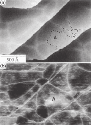
stant-current scan. Figure 15–31 shows STM and BEEM current images
obtained on 2.5 nm epitaxial CoSi
2
/Si(111) (Sirringhaus et al., 1994). The
lattice mismatch of 1.2% between the metallic silicide and the Si sub-
strate is accommodated by an interfacial dislocation network. In STM
topography, the location of these line defects is detected via their elastic
strain fi eld at the CoSi
2
surface. Strikingly, the defects are mapped in
BEEM as sharply localized regions with increased collector current
with a width of only 0.8 nm, as expected for ballistic transport of car-
riers with a strongly forward focused tunneling momentum distribu-
tion, i.e., k
||
∼ 0. While the Schottky barrier was found to be uniform,
as expected for an epitaxial interface, the sharp local increase in trans-
missivity of the CoSi
2
/Si interface was explained by a signifi cant
increase in in-plane momentum due to scattering by the dislocation
core, facilitating the transmission into the Si conduction band
minima.
Figure 15–31. (a) Constant-current
STM image and (b) corresponding
BEEM image obtained on epitaxial
2.5 nm CoSi
2
/Si(111). A dislocation
network at the silicide/silicon inter-
face is indicate by dashed lines. In
the BEEM image brighter areas
indicate regions of higher collector
current. Hot electron scattering at
the interfacial dislocations causes a
sharply localized increase in collec-
tor current.
Chapter 15 Scanning Tunneling Microscopy in Surface Science 1011
In experiments such as those on CoSi
2
/Si(111), growth and probing
of the entire heterostructure in the same UHV environment is critical
to achieve ordered interfaces and reliable measurements on reactive
metal surfaces. For the microscopy itself, low temperatures have several
practical advantages, such as improved energy resolution due to
reduced thermal broadening of the tunneling distribution, and reduced
thermal drift of the STM. An additional benefi t is a lower thermal noise
due to a reduction of thermionic emission across interfacial barriers,
which allows shallower potential barriers to be probed. As a result,
semiconductor band offsets, resonant transport in semiconductor het-
erostructures, and interfacial barriers between an organic layer and a
metal base (Troadec et al., 2005) can be measured successfully by low-
temperature BEEM. Examples are embedded self-assembled quantum
dots (Rubin et al., 1996), lithographically patterned quantum wires
(Eder et al., 1996), double-barrier resonant tunneling structures (Sajoto
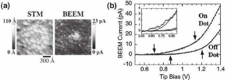
et al., 1995), and superlattices (Heer et al., 1998). Figure 15–32 shows
the band profi le for carrier injection into an individual InAs quantum
dots in GaAs (Rubin et al., 1996). Also shown are STM and BEEM
images, as well as BEEM spectra obtained with the tip positioned on
top and next to the dot. The semiconductor heterostructure was coated
with a polycrystalline Au base layer, whose morphology largely domi-
nates the contrast in STM. A strong enhancement in BEEM current in
a circular region with 30 nm diameter is associated with carrier trans-
port through a single InAs quantum dot. A comparison of BEEM
spectra obtained on and between dots shows signatures of transport
through two zero-dimensional states of the dot.
Ballistic carrier transport and scattering can, in principle, be used
to probe a wide variety of other systems, beyond Schottky barriers
and semiconductor heterostructures. Examples are metal–insulator–
semiconductor structures (Cuberes et al., 1994) or magnetic multilayers
(Rippard and Buhrmann, 2000). In the latter, an Au/Si(111) Schottky
barrier is used as an analyzer for spin-dependent scattering of carriers
Figure 15–32. BEEM on self-assembled quantum dots. (a) STM and BEEM images of an individual
InAs/GaAs quantum dot under a polycrystalline Au base. (b) Comparison of BEEM spectra obtained
by ballistic electron injection into an InAs dot and into the wetting layer between dots. (Reprinted
with permission from Rubin et al., © 1996 by the American Physical Society.)
1012 P. Sutter
in a Co/Cu/Co trilayer structure, used in spin-valve devices, inte-
grated on top of the Au base layer. Unpolarized carriers injected from
an STM tip into this magnetic multilayer base will undergo spin-
dependent scattering in the ferromagnetic Co layers. In areas in which
the Co layers couple ferromagnetically, only one spin component will
be scattered heavily and a large fraction of unscattered carriers is
transmitted across the Au/Si interface. If the magnetization direction
of the two Co layers is misaligned, both spin components are strongly
attenuated by scattering, causing a sharp drop in collector current.
5.2 Probing Buried Interfaces (II)—Quantum Size Effects
In BEEM hot carriers, locally injected into a metal/semiconductor het-
erostructure, are used to measure the transmitted current across a
buried interface. Instead, carriers that impinge with energies below
threshold and are refl ected back into the metal fi lm can also be con-
sidered. Due to the long mean free path, these carriers can set up
standing waves in the metal fi lm. An STM tip, probing the evanescent
tails into the vacuum, can then be used to image fringes due to inter-
ference of these electrons. The concept of electron interference in metal
fi lms dates back to Jaklevic et al. (1971), and interference effects have
been observed by angle-resolved photoemission, low-energy electron
diffraction and low-energy electron microscopy.
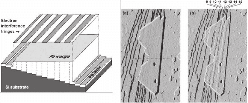
An implementation of an STM experiment to probe interference
effects in the system Pb/Si(111) is shown in Figure 15–33. Pb evapo-
rated onto a stepped Si(111) substrate forms (111)-oriented islands
whose surface is atomically fl at. Due to the substrate vicinality, the Pb
Figure 15–33. Electron interference in a Pb “quantum wedge” on Si(111). (Left) Geometry of the
Pb wedge on a stepped Si(111) substrate. The Pb thickness varies in increments of roughly one Si(111)
step height, giving rise to electron interference fringes in the direction of the substrate steps. (Right)
Constant-current STM images (730 nm × 110 0 n m) at −5 V (a) and +5 V (b) sample bias. The image
obtained at positive bias shows apparent height changes at the surface of the wedge due to electron
interference in the Pb fi lm. (Reprinted with permission from Altfeder et al., © 1997 by the American
Physical Society.)
Chapter 15 Scanning Tunneling Microscopy in Surface Science 1013
island is wedge shaped, with a thickness that changes in integer mul-
tiples of the Si(111) step height from one substrate terrace to the next.
While STM at positive sample bias, i.e., injection of electrons from the
tip, images the atomically smooth Pb surface, STM images at opposite
bias show bands of apparent terraces and steps, aligned with steps of
the Si substrate, at the surface of the Pb wedge. These images, and
associated tunneling spectra, are interpreted as signatures of quantum
well states in the Pb wedge (Altfeder et al., 1997), and can be used to
determine the position of subsurface steps as well as the position-
dependent absolute thickness of the Pb fi lm. Bands with constructive
and destructive interference alternate with a thickness change d
0
of one
Pb(111) monolayer if d
0
≈ λ
F
/4, where λ
F
denotes the Fermi wavelength.
Similar interference effects were also observed by STM for epitaxial
silicide layers, such as CoSi
2
/Si(111) (Lee et al., 1994) and NiSi
2
/Si(111)
(Kubby and Greene, 1992).
Strikingly, electron interference can even be used to image interfacial
atomic structures buried under as much as 10 nm of metal. In the Pb/
Si(111) system, the (7 × 7) reconstruction of the Si(111) surface remains
essentially intact upon low temperature evaporation of Pb, except for
some intermixing by replacing Si adatoms by Pb (Altfeder et al., 1998).
Due to the topology of the Fermi surface of Pb, in particular a large
mismatch between the electron effective mass in in-plane and normal
directions, the quantized electron states in the Pb fi lm can be used to
map interfacial structure with a resolution of 0.6 nm for overlayer thick-
nesses exceeding 10 nm, or roughly 10 times the Fermi wavelength in
the metal.
5.3 Imaging Buried Heterostructures—Cross-Sectional STM
The strong interest in low-dimensional semiconductor structures—
quantum wells, wires, and dots—has stimulated widespread activity
in nanoscale imaging of electronic materials with reduced dimension-
ality. Recent efforts have focused on self-assembled quantum dots,
generated by lattice mismatched heteroepitaxial growth. Semiconduc-
tor quantum dots with lateral size in the 10–100 nm range are readily
imaged by STM if they are exposed as islands on a free surface. Con-
sequently, a large number of studies have been devoted to studying
epitaxial growth and quantum dot self-assembly by conventional STM
imaging. However, almost any technological applications of self-
assembled quantum dots require embedding in a matrix, often consist-
ing of the substrate material. The embedding process causes signifi cant
modifi cations to the dots that include segregation and intermixing,
shape changes, dopant redistribution, and adjustments to the local
strain fi eld in the dot and in the surrounding material. All these
factors make it desirable to image embedded rather than exposed
nanostructures.
Cross-sectional STM (X-STM), originally demonstrated by Feenstra
et al. (1987) for imaging and spectroscopy on (110) surfaces of III–V
compound semiconductors, offers an elegant solution to this chal-
lenge. Semiconductors that cleave easily, as most III–V compounds do,
1014 P. Sutter
are used as a substrate for the growth of embedded self-assembled
quantum dots. A sample is then cleaved in UHV, and STM imaging is
performed on the cleavage face, typically a nonpolar (110) plane, which
provides large step-free areas for atomic resolution imaging. In this
geometry, X-STM gives access to subsurface structures over the entire
thickness of the epitaxial layer and the underlying substrate.
X-STM has been used to image a variety of buried semiconductor
heterostructures, such as superlattice structures in GaAs/AlGaAs
(Salemink and Albrektsen, 1991), InAs/GaSb (Feenstra et al., 1994), and
GaN/GaAs (Goldman et al., 1996), showing atomic-scale composition
fl uctuations, interface roughness, lateral stain variations, and phase
separation in these systems. The technique has seen a strongly revived
interest with the advent of self-assembled quantum dots and quantum
dot superlattices (Legrand et al., 1998). Specifi cally for the imaging of
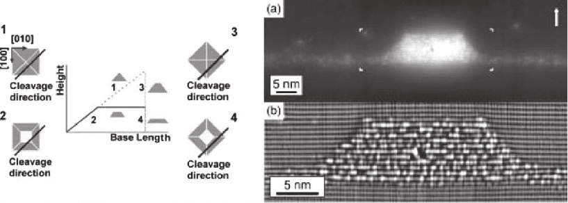
quantum dots, X-STM relies on the fact that the dots are small and form
rather dense populations. Hence, a random cleavage will cut through
a large number of these nanostructures and provide a cross-sectional
view of their atomic structure on the cleavage plane (Figure 15–34).
Much of the power of X-STM imaging derives from the fact that bias-
dependent imaging provides chemical contrast on (110) cleavage faces
of III–V compounds (Feenstra et al., 1987). Empty-state imaging gives
atomically resolved maps of the cation sublattice and allows a direct
identifi cation of atomic species, e.g., indium atoms in a GaAs matrix
(Pfi ster et al., 1995). This electronic structure effect not only provides
strong contrast to determine the shape of individual buried InAs
quantum dots and their stacking in multilayer structures, but can also
be used to quantify interface roughness, intermixing, and surface seg-
regation, near the dots and the wetting layer, with atomic precision.
To access this information in high-resolution images, a background
subtraction has to be performed to remove topographic contrast of the
Figure 15–34. Cross-sectional STM on self-assembled quantum dots. (Left) Illustration of the possible
apparent geometries observed due to cleavage at random positions through quantum dots with pyra-
midal and truncated pyramidal shape. (Right) Filled-state constant-current STM of an InAs quantum
dot embedded in GaAs. Part of the image in (a) is treated by a local mean equalization fi lter to accen-
tuate the atomic corrugations in the dot and the surrounding GaAs matrix, as shown in (b). (Reprinted
with permission from Bruls et al., © 2002 American Institute of Physics; reprinted with permission
from Gong et al., © 2004 Amercian Institute of Physics.)
Chapter 15 Scanning Tunneling Microscopy in Surface Science 1015
pronounced local deformation of the cleavage plane due to the relax-
ation of the strained dots and matrix (Davies et al., 2002). Conversely,
when combined with modeling, the elastic relaxation at the free cleav-
age surface itself can be used to quantitatively determine the strain
fi eld in and around individual dots.
Apart from the imaging of buried semiconductor quantum struc-
tures, an application of X-STM that has been receiving increasing atten-
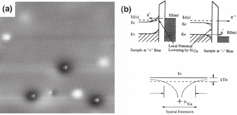
tion is the mapping of electronic dopants for electronics (Figure 15–35)
and, more recently, of magnetic dopants for spintronics applications.
Buried substitutional Zn and Be acceptors in p-GaAs have been imaged
as protrusions in fi lled-state constant-current STM via a contrast mech-
anism assigned to an increased local state density directly above a
dopant (Johnson et al., 1993). Si donors at Ga sites (Si
Ga
) in GaAs have
been imaged on GaAs(110) as protrusions, a few nanometers in size
and with discrete values of apparent height, superimposed on the
background lattice. The observed contrast in fi lled-state constant
current STM was attributed to a local perturbation of the near-surface
band bending by the Coulomb potential of the Si
Ga
. The discrete appar-
ent heights were interpreted as a consequence of a distribution of the
donor atoms over fi ve subsurface layers beneath the cleavage surface
(Zheng et al., 1994).
Deep acceptor states due to magnetic impurities in III–V semicon-
ductors, such as substitutional Mn
Ga
in GaAs, are expected to play an
important role in the hole-mediated coupling between magnetic impu-
Figure 15–35. Imaging of individual dopants by X-STM. (a) Filled-state constant-current STM image
(V = −1.6 V) of cleaved GaAs(110). Individual Si
Ga
substitutional donors appear as protrusions of dif-
ferent apparent height. (b) Band diagram illustrating the electron tunneling process between a metal
tip and the GaAs(110) surface in the presence of tip-induced band bending. The Coulomb potential of
a donor ion locally alters the band bending, causing an increase in tunneling current above the donor.
(Reprinted with permission from Zheng et al., © 1994 by the American Physical Society.)

1016 P. Sutter
rities, and thus determine the magnetic properties of hole-mediated
ferromagnetic semiconductors such as Ga
1−x
Mn
x
As, important for
emerging spintronics applications. X-STM at room temperature was
used to map the wave function of the hole bound to an individual Mn
acceptor in GaAs (Yakunin et al., 2004). Via bias-induced changes to
the local band bending, the acceptor could be imaged in both the
neutral (U
S
= +0.6 V) and ionized state (U
S
= −0.7 V). The acceptor
ground state has a highly anisotropic structure due to a signifi cant
contribution of d-wave envelope functions, which is well-reproduced
by simulated images based on a tight-binding model of the Mn accep-
tor structure (Tang and Flatté, 2004).
6 STM Image Simulation
Although STM is a very powerful experimental technique in its own
right, geometric and spectroscopic contrast tend to be diffi cult to sepa-
rate, as discussed previously. In many cases, the unequivocal identifi -
cation of surface structures or of adsorption geometries requires a
comparison of experimental STM images with contrast simulations.
The conventional approach to STM image simulations follows a two-
step process. Relaxed atomic positions of candidate surface structures
are calculated by ab initio theoretical methods, such as density func-
tional theory. The actual STM contrast is then computed using the
Tersoff–Hamann theory of STM (Tersoff and Hamann, 1983, 1985).
By combining bias-dependent atomic-resolution STM images with
simulated images for various candidate structures, even completely
unknown surface structures can in principle be “solved” on the basis
of STM imaging alone. The diffi culty lies less with the microscopy than
with the identifi cation of plausible candidate surface structures. In the
past, this key step has typically been approached intuitively, i.e., by
guessing structures based on minimizing the density of dangling
bonds, starting from a truncated bulk structure. Recently developed
systematic techniques, based on stochastic optimization, for generating
comprehensive sets of candidate structures promise to become a pow-
erful tool for solving a wide range of surface structures by STM imaging
and image simulation (Ciobanu and Predescu, 2004).
The Tersoff–Hamann theory, the basis of most STM image simula-
tions to date, provides a transfer matrix formalism to calculate the
tunneling matrix element and tunneling current for realistic confi gura-
tions of tip and sample. For values of tip–sample separation typical in
STM imaging (∼1 nm), the coupling between tip and sample wave func-
tions is weak, and the tunneling process can be treated by fi rst-order
perturbation theory. Within this framework the tunneling current is
given by
I
e
fE fE M E V E
eV
=
(
)
−
(
)
[]
+−
(
)
≈
∑
2
2
2
π
δ
π
µν
µν
µν ν µ
,
MMEEEE
FFµν µ ν
µν
δδ
2
−
(
)
−
(
)
∑
,
(7)

Chapter 15 Scanning Tunneling Microscopy in Surface Science 1017
where f(E) is the Fermi function, V denotes the tunneling bias, M
µv
the
tunneling matrix element between a tip state ψ
µ
and a sample state ψ
v
,
and E
µ(v)
the energy of state ψ
µ(v)
. In the second line, the Fermi function
was replaced by a step function (zero-T approximation), and the limit
of low tunneling bias has been assumed. If, after Bardeen (1961), the
tunneling matrix element is written as a surface integral, and the
sample and tip wavefunctions are expanded in plane waves, one
obtains
M
m
dabe e
v
z
i
t
µ
κ
π
=−
∫
−
⋅
4
22
q
qq
q
*
qx
t
(8)
Here q is the Fourier wavevector and a
q
, b
q
are expansion coeffi cients
in the plane wave expansion of the sample and tip wavefunctions, x
t
and z
t
denote the lateral and vertical tip position, and κ
q
is the decay
constant. Given the wavefunctions of sample and tip, this expression
provides the tunneling matrix element, from which the tunneling
current can be calculated via Eq. (7).
In practice, a diffi culty arises from the fact that the atomic-scale
geometry and chemical composition of the tip are unknown. Thus,
assumptions have to be made as to the tip wavefunctions (i.e., b
q
). For
an s-wavefunction of the tip (as for an ideal “point”–tip), the tunneling
current is
IEEE∝
()
−
(
)
≡
()
∑
ψδ ρ
ν
r
tt
r
2
vF F
,
(9)
i.e., is proportional to the local density of states of the sample at the
Fermi energy, a property of the sample surface alone! For fi nite tun-
neling bias, V, the tunneling current can be written as an integral over
the energy range between the Fermi energy E
F
and E
F
+ V:
IEEeVTEeVdEt
eV
=
()
−
()()
∫
ρρ
ts
0
, (10)
and the tunneling conductance at bias V is proportional to the posi-
tion-dependent density of states of the sample at energy eV from the
Fermi energy
dI
dV
eV T eV V
V
(
)
≈
()()( )
ρρ
ST
0,
(11)
Contrast calculations thus involve the computation of the position- and
energy-dependent sample DOS to obtain simulated maps of tunneling
conductance dI/dV(x,y) or tunneling current I(x,y).
Although originally derived for small voltages, as used for STM
imaging on metals, with this extension the Tersoff–Hamann formalism
can be applied to simulate images at higher bias as well, and has
proven a powerful simulation tools for a wide range of imaging sce-
narios. Tromp et al. (1986) were the fi rst to show that it could be applied
to semiconductor surfaces, as demonstrated by their successful contrast
simulation for the Si(111)-(7 × 7) reconstruction. The systems simulated
since then include surface structures of semiconductors (Fujikawa
et al., 2002; Klijn et al., 2003), ultrathin insulators (Olsson et al., 2005),
1018 P. Sutter
as well as adsorbed atoms (Repp et al., 2004) and molecules (Olsson et
al., 2003; Kühnle et al., 2002).
Figures 15–36 and 15–37 illustrate two of the numerous examples of
this approach in the literature.
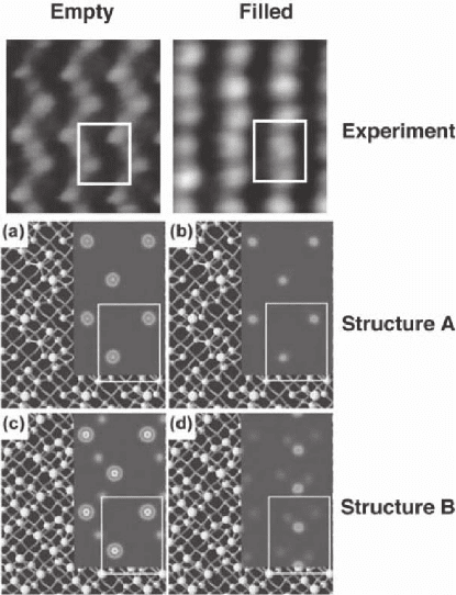
Shallow Ge quantum dots self-assembled during heteroepitaxy on
Si(001) invariably have surface termination by (105) facets, with surface
normal just 11° away from [001]. These (105) facets appear extremely
stable, likely due to a low density of dangling bonds and additional
strain stabilization by surface strain compensating for some of the 4%
lattice mismatch strain between the Ge overlayer and the Si substrate.
To calculate the surface energy, and thus explain the stability of the
facet, a detailed knowledge of the surface structure is necessary. Dual
bias constant-current STM combined with STM contrast calculations
was used to identify a best match with one of two proposed structures
of the (105) surface: “paired dimer” (Structure A) and “rebonded step”
(Structure B) (Fujikawa et al., 2002). The STM contrast is clearly identi-
fi ed as that of a “rebonded step” structure, the structure that not only
has the lowest dangling bond density but also causes tensile surface
strain, key to the strain stabilization of the (105) facet.
Figure 15–36. Identifi cation of the surface structure of Ge(105). Empty- and
fi lled-state constant-current STM images are compared with two candidate
structures, the paired dimer Structure A and rebonded step Structure B (c and
d). A Tersoff–Hamann calculation of the STM contrast for these two structures
clearly shows that the experimental STM images arise from the rebonded step
structure. (Reprinted with permission from Fujikawa et al., © 2002 by the
American Physical Society.)
Chapter 15 Scanning Tunneling Microscopy in Surface Science 1019
Simulations of STM contrast of adsorbed molecules pose a somewhat
different problem than simulations of surface structures. For solid
surfaces, the combination of STM imaging with image simulation can
discriminate between several candidate structures, as discussed in the
previous example. For molecules, the structure is typically well known.
However, the adsorption geometry (site, orientation) as well as the
conformation for larger, more fl exible molecules enter as unknowns
into the simulation. A relatively simple example is the stiff molecular
cage structure of fullerene C
60
(Hou et al., 1999; Pascual et al., 2000; Lu
et al., 2003). In this case, the structure and conformation are well
known, and the only parameter of the contrast calculation is the ori-
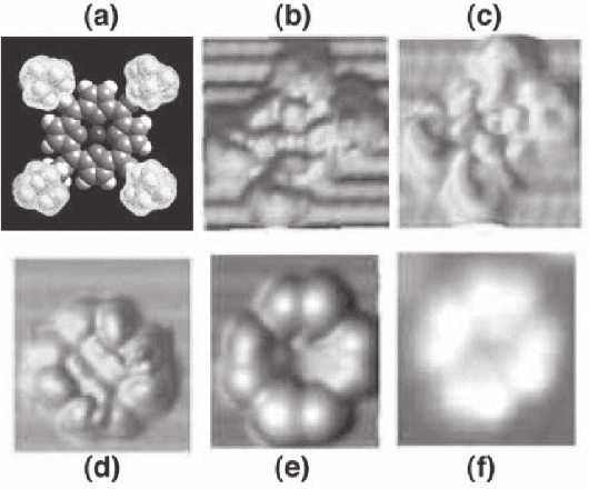
entation. A more complex system, Cu-tetra(3,5-di-tert butyl phenyl)
porphyrin (Cu-DTBPP) on Cu(211), is illustrated in Figure 15–37.
Cu-DTBPP consists of a central porphyrin ring with four symmet-
rically attached di-tert-butyl phenyl (DTBP) groups (Figure 15–37a).
These four bulky groups determine the shape of the molecule, which
is imaged in STM as a four-leaf clover structure, and defi ne the interac-
tion with the metal substrate (Jung et al., 1996). The orientation of the
side groups is the main parameter that needs to be optimized to deter-
mine the conformation of the adsorbed molecule, and to simulate the
experimental STM images. Figure 15–37 shows several candidate con-
formations, with leg angles of 60° (b), 45° (c), 30° (d), and the optimized
angle of 10° relative to the substrate (e), which was found to best repro-
duce the experimental STM image of the molecule.
Figure 15–37. Identifi cation of the molecular conformation of Cu-DTBPP on
Cu(211). (a) Molecular model of Cu-DTBPP, with the four-lobed pattern
observed by STM marked in yellow. (b–e) STM contrast calculation for differ-
ent angles between the four legs and the substrate: (b) 60°, (c) 45°, (d) 30°, and
(e) 10°. (f) Experimental STM image of the molecule. (Reprinted from Moresco
et al., ©2002 with permission from Elsevier.) (See color plate.)
