Ghodssi R., Lin P., MEMS Materials and Processes Handbook
Подождите немного. Документ загружается.

794 A.D. Raisanen
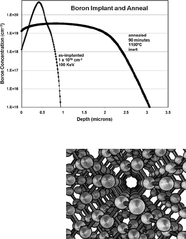
Fig. 10.32 ATHENA simulation of boron implantation and subsequent anneal. Note non-Gaussian
implanted distribution and long-range diffusion
Fig. 10.33 Channel-through
silicon crystal structure. Ion
propagation down these
channel directions results in
deeper implant profiles than
expected from simple models
secondary knock-on collisions, each displacing atoms from their equilibrium lat-
tice positions where they can induce a variety of acceptor, donor, and trap electronic
levels. Ions implanted into a lattice will generally come to rest in a variety of intersti-
tial positions incompatible with acting as electrically active dopants. Atoms on the
surface of the crystal, either from contamination or from structures formed on the
surface, can be struck by incoming ions and end up implanted deep in the substrate
by elastic collision. At high ion doses entire layers of the lattice can be rendered
amorphous. The damage to the lattice due to ion collisions must be repaired by
some type of thermal process in order to activate t he dopant concentration.
10 Doping Processes for MEMS 795
Layers that have been rendered completely amorphous are generally easier
to recrystallize and activate than layers which have been damaged but not ren-
dered amorphous. Typical implant doses required to produce an amorphous layer
are 1 × 10
15
cm
−3
and up. When annealed, a fully amorphous layer will begin
assembling a new crystal structure using undamaged crystalline silicon below the
amorphous layer (or even above it if the implant was well below the surface) as a
template, in a process known as solid-state epitaxy. Excellent recrystallization can
often be obtained at temperatures below 600
◦
C if the damaged layer is rendered
fully amorphous. This effect can be accomplished intentionally without doping [65]
by implanting nondopant species such as argon or silicon into a silicon substrate.
Sometimes an amorphous layer will be intentionally formed at a silicon surface
to inhibit channeling. Channels are sealed when the crystal order near the sur-
face is destroyed, allowing implants to be performed for shallow junctions without
channeling tails.
10.5.5 Buried Insulator Layers
An interesting application of implant technology is in the production of silicon-
on-insulator wafers used in a variety of electronics and MEMS applications. Two
competing technologies exist, both of which depend on implantation of a heavy ion
dose well below the surface of a silicon wafer.
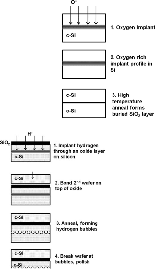
In the SIMOX (separation by implantation of oxygen) process illustrated in
Fig. 10.34, a very high dose (>1.8 × 10
18
cm
−2
) of oxygen ions is implanted at
high energy (200 keV or better) in a single-crystal silicon wafer. The implanted
wafer is annealed to more than 1300
◦
C to eliminate crystal damage from the ion
implantation and to drive formation of a buried oxide insulating layer. This results
in a thin crystalline silicon layer isolated from the bulk silicon wafer, which can be
used for released MEMS structures or transistors [66].
A related process is the SmartCut
TM
process (Fig. 10.35), which begins with
a single-crystal silicon wafer coated with thermal oxide. Hydrogen or helium is
implanted through the oxide to a specific depth below the silicon surface. Typical
hydrogen ion doses of > 3.5 × 10
16
− 1 × 10
17
are required. Once implanted, a
second silicon wafer is bonded to the oxide layer, and the wafer undergoes a series
of anneals that results in voids and blistering in the implanted zone. The implanted
layer breaks free from the underlying donor silicon wafer, resulting in a silicon
wafer with a second layer of single-crystal silicon separated by the original thermal
oxide layer [67]. Both of these processes are only made possible by the ability of
ion implantation doping to deposit ions at a controlled depth below the substrate
surface.
10.5.6 Case Study: Heavily Doped Polysilicon
A project to fabricate thin-film polysilicon resistive heater elements as part of a
microscopic MEMS infrared target array required heavily doped polysilicon with
796 A.D. Raisanen
Fig. 10.34 SIMOX process
for production of SOI wafers
Fig. 10.35 SmartCut process for production of SOI wafers
good resistance uniformity across a six-inch wafer. Spin-on dopant sources and ion
implantation were chosen as candidate processes to dope the polysilicon.
Six-inch (100) wafers were prepared with a 2 μm thick plasma-enhanced
TEOS oxide deposition to act as electrical and thermal insulation. Polysilicon was
deposited using a low-pressure chemical vapor deposition tube. The tube process

10 Doping Processes for MEMS 797
temperature is ramped with an increase in t emperature from the load/gas injection
end to the source/pump end, from 635
◦
C at the entrance, to 650
◦
C at the center
where the wafers are located, and 665
◦
C at the output. A 100 sccm flow of SiH
4
is injected at the load end, and the pressure is controlled to 300 mtorr by a throttle
valve during the process. These conditions produce a polysilicon deposition rate of
110 Å/min.
All wafers were coated with a nominally 4000 Å polysilicon deposition. The
coated polysilicon wafers were measured with a Nanospec
TM
spectroscopic reflec-
tometer after coating. Four doping treatments were then performed.
Wafer 1 Spin on Borofilm-100 liquid dopant from Emulsitone Corp (Whippany, NJ) at
3000 rpm for 30 s, and bake at 200
◦
C for 15 min in a convection oven to remove
solvents. Anneal in diffusion tube in N
2
ambient for 55 min at 950
◦
C, then anneal in
O
2
ambient for an additional 5 min at 950
◦
C. Strip oxide film in 10:1 HF solution.
Wafer 2 Spin on N-250 Emitter Diffusion Source liquid dopant from Emulsitone Corp
(Whippany, NJ) at 3000 rpm for 30 s, and bake at 200
◦
C for 15 min i n a convection
oven to remove solvents. Anneal in diffusion tube in N
2
ambient for 25 min a t
950
◦
C, then anneal in O
2
ambient for an additional 5 min at 950
◦
C. Strip oxide film
in 10:1 HF solution.
Wafer 3 Implant dose 1 ×10
16
Boron-11 at 35 keV energy. Anneal in diffusion tube in N
2
ambient for 25 min at 950
◦
C, then anneal in O
2
ambient for an additional 5 min at
950
◦
C. Strip oxide film in 10:1 HF solution.
Wafer 4 Implant dose 1 ×10
16
Phosphorus-31 at 100 keV energy. Anneal in diffusion tube in
N
2
ambient for 25 min at 950
◦
C, then anneal in O
2
ambient for an additional 5 min
at 950
◦
C. Strip oxide film in 10:1 HF solution.
Polysilicon thicknesses were measured again after the oxide strip so that actual
bulk resistivities could be computed with the thicknesses corrected for any material
lost to oxidation. An automated four-point probe system was used to measure the
polysilicon sheet resistance for each wafer. The results are shown below.
Wafer
Initial thickness
(Å)
Final thickness
(Å)
Sheet resistance
(/sq)
Resistance
uniformity (%)
Resistivity
cm
1 3979 3663 164.5 3.9 6.0 × 10
−3
2 4007 3572 158.3 10.2 5.7 × 10
−3
3 4049 3907 152.2 1.4 5.9 × 10
−3
4 4059 3880 81.1 1.6 3.1 × 10
−3
All four treatments obtained quite high doping levels suitable for our purposes.
Resistivity uniformity for the spin-on dopant processes was somewhat inferior to the
ion implantation results. The more costly ion implantation process was selected for
this project, as resistance uniformity was critical. For applications requiring heavily
doped polysilicon with less stringent resistivity requirements, the spin-on dopants
produce quite comparable r esults at significantly lower process cost and complexity.
798 A.D. Raisanen
10.6 Plasma Doping Processes
Ion implantation processes are very effective at producing tailored dopant profiles
with a high degree of control over dose and depth profile, while maintaining compat-
ibility with a very broad selection of masking techniques. Unfortunately, one major
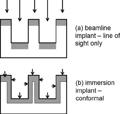
disadvantage of conventional ion implant technology is the line-of-sight limitation
imposed by the generation and transport of the dopant ion beam. Implantation of
deep trench sidewalls, for instance, cannot be performed, and shadowing effects
produced by large topographies, as often encountered in MEMS devices, can result
in serious doping level nonuniformities. A second shortcoming of conventional
implant technologies is in the difficulty of producing large beam currents at low
kinetic energies, useful for producing very shallow junction depths for modern
deep-submicron integrated circuitry.
A relatively new doping process has been developed specifically to address these
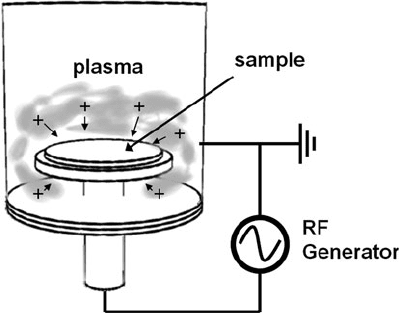
shortcomings, called plasma doping or plasma immersion ion implantation [68, 69]
(See Fig. 10.36). This process places substrates to be treated in a vacuum chamber
and immerses the substrate in a plasma discharge rich in dopant ions. The plasma
can be generated with a variety of methods, with electron cyclotron resonance and
inductively coupled sources being popular. A bias is applied to the substrate by
imposing a DC voltage (in the case of electrically conductive substrates) or by
applying a radio frequency or pulsed voltage.
Fig. 10.36 Plasma
immersion ion implantation
schematic
Much as is seen in reactive ion etch processes, a negative bias is developed on
the substrate surface as a consequence of the large difference in electron versus ion
mass and mobility [70]. Positively charged ions in the plasma then bombard the
negatively biased substrate, resulting in implantation of the ionized species. In con-
trast to conventional beamline ion implantation processes that typically deliver ions
at 10 keV or more, the ions in the plasma impact the substrate surface at a rela-
tively low energy, 100–5000 eV, which can be adjusted by varying the RF bias on
the wafer. The plasma chemistry is chosen to be rich in the desired dopant species,
10 Doping Processes for MEMS 799
such as BF
3
to obtain boron ions and PH
3
to obtain phosphorus. The induced RF
bias accelerates plasma ions relatively perpendicular to the substrate surface, thus
there is no problem in doping wafers with large topographies problematic for con-
ventional beam implant techniques. Even high-aspect-ratio deep trenches can be
successfully doped [71] as illustrated schematically in Fig. 10.37.
Fig. 10.37 Plasma
immersion ion implantation
of three-dimensional structure
sidewalls
Trenches etched in silicon with up to 25:1 aspect ratio implanted with boron ions
from a BF
3
plasma show about a 2:1 enhancement of sheet resistivity between the
bottom of the trench and the s idewall, indicating some anisotropy in narrow struc-
tures but remarkably good ability to dope vertical structures [69]. The small size
of the trenches prevents ions from being extracted from the plasma sheath perpen-
dicular to the trench sidewall, but ions moving in the vertical direction undergo
reflections and collisions that result in large ion doses being delivered to the side-
wall surfaces at shallow angles where they can be adsorbed. These surface ions are
transported to the bulk silicon by knock-on collision processes and electron excited
diffusion. At higher ion energies, this angle of incidence for ion delivery becomes
more and more vertical, resulting in a loss of implant current to the sidewalls relative
to the bottom of the trench [69].
The combination of low implant energy and rapid thermal processing techniques
for activation can produce extremely shallow junctions for advanced CMOS devices
[72, 73]. Junction depths of 100 nm or less are obtainable for wafer DC biases of
5 kV or less after rapid thermal annealing to 1050
◦
C for 10 s [73]. Little or no
etching of silicon or damage to sensitive gate oxide structures is observed.
Plasma doping processes are capable of delivering ion currents an order of
magnitude higher than most conventional ion implant machines, offering signifi-
cant throughput advantages for high-dose applications. Fabrication of silicon-on-
insulator wafers using SIMOX and SmartCut processes, with oxygen and hydrogen
implanted species, respectively, have been demonstrated [73].
800 A.D. Raisanen
One significant difference between beamline implants and plasma immersion
implants is potentially in the purity of the implanted species. Inasmuch as immer-
sion implant systems lack any means of filtering out different ion masses or energies,
a distribution of ion energies is injected into the substrate surface, leading to some
broadening of the implanted dopant profile relative to monoenergetic beamline pro-
cesses. All positively charged species in the plasma are implanted into the substrate
to some extent, leading to somewhat higher levels of contamination relative to beam
line processing. However, species such as fluorine in a BF
3
plasma generally have
little effect from a doping standpoint, so plasma implant processes are regarded as
being potentially as clean as beamline implant processes as long as materials used
in fixturing and chamber walls are compatible.
One of the major uses of plasma immersion implant is in surface treatments.
Conventional beamline implants cannot effectively treat the surfaces of complex
structures due to the strict line-of-sight requirement. Tribological properties of many
metals can be improved by implanting very large doses of carbon, nitrogen, or other
dopant species into the surface [74]. These surfaces exhibit enhanced wear resis-
tance, making them valuable in applications such as bearing s urfaces in machine
tools, molding tooling, and biomedical implants. Large ion currents delivered to
surfaces can go beyond simple doping and actually alter the chemical nature of a
surface by driving reactions such as oxidation or nitridation, allowing synthesis of
these films on sensitive surfaces that would not withstand more conventional ther-
mal synthesis techniques [74, 75]. For example, significantly enhanced resistance
to biofouling has been reported on metal oxide surfaces synthesized by immersion
implant [75], an important parameter for implantable medical devices.
10.7 Dopant Activation Methods
Dopants introduced during crystal growth or high-temperature diffusion methods
are fully incorporated into the crystal matrix and immediately contribute to the
electron and hole concentration of the crystal. Dopants introduced from outside by
ballistic processes such as ion implantation are unlikely to occupy the correct lattice
or interstitial sites in order to contribute to the free carrier inventory of the crystal.
Instead, they occupy defect or interstitial sites that simply act as scattering centers
and decrease the mobility of carriers in the crystal. The process of reordering the
semiconductor crystal to properly incorporate dopants so they contribute electrons
and holes to the matrix is known as activation.
10.7.1 Conventional Annealing Methods
The most straightforward activation process is simple thermal annealing. The sub-
strate is heated to a sufficiently high temperature to mobilize crystal and dopant
atoms, and it is maintained at that temperature for a time sufficient to regrow the
10 Doping Processes for MEMS 801
crystal structure with the dopants incorporated. The equipment required for conven-
tional annealing is relatively modest, typically consisting of a three-zone diffusion
furnace with quartz liner like the one illustrated in Fig. 10.25. The atmosphere
of an annealing furnace is often an inert ambient such as N
2
or Ar, but often an
oxidizing ambient of O
2
or steam is introduced to suppress autodoping effects
(dopants migrating from wafer to wafer or from process fixturing to wafers) or
to modify the final doping profile by oxidation redistribution of dopants at the
surface.
The primary disadvantage of this process is the requirement for extended periods
at elevated temperatures, which allows dopants to diffuse for a long distance. This
limits the ability to produce junctions of an arbitrarily shallow profile. The high
thermal budget also limits materials’ compatibility for MEMS devices to those that
can withstand extended periods at the high temperature.
The temperature and time required for dopant activation and crystal damage
repair depend critically on the amount of damage done by an implant process,
which varies with the implant dose and implant species. In general, implant dam-
age at low total dose, below 1 × 10
12
cm
−2
, can be easily removed by an anneal
of about 600
◦
C due to the small number of atoms displaced from their normal lat-
tice positions. If a crystal structure has become fully amorphous, for implant doses
of about 1 × 10
15
cm
−2
or higher, annealing the damage can also be performed
at the relatively low process temperature of 600
◦
C. In this case, the amorphous
layer regrows using the underlying crystal structure as a template via the solid-
phase epitaxy process. Complexes of buried defects remain at the boundary between
the amorphous and crystalline zone after annealing which can affect electrical
devices using this region, but in general very high levels of dopant activation can be
obtained [7].
For ion implantation doses between about 1 × 10
13
− 1 × 10
15
, damage to the
crystal will be increasingly severe, but the crystal retains a recognizable structure
that will compete with solid-phase epitaxy for regrowth. Silicon atoms displaced
from their normal lattice sites can condense into extended defect structures that are
difficult to break up and reintegrate into a pristine crystal structure. Annealing tem-
peratures of up to 1050
◦
C can be required to rebuild the crystal structure and provide
a high degree of dopant activation in these heavily damaged crystals. Unfortunately,
these high-temperature conventional anneals drive large amounts of diffusion of the
dopant species, making formation of shallow doped layers problematic, as illus-
trated in Fig. 10.32. If a shallow junction is desired and only conventional thermal
annealing processes are available, it is often a good strategy to implant a high
dose (5 × 10
15
cm
12
or higher) of Ar or Si to render the s urface or buried region
fully amorphous before implanting with the desired dopant species. The amor-
phous layer can then be annealed at relatively low temperature via solid-phase
epitaxy. Fortunately, for many MEMS processes it is desirable to have substan-
tial movement of dopants during diffusion, such as the formation of a boron etch
stop for a 20 μm thick diaphragm, so inexpensive thermal processes are heavily
utilized.
802 A.D. Raisanen
10.7.2 Rapid Thermal Processes
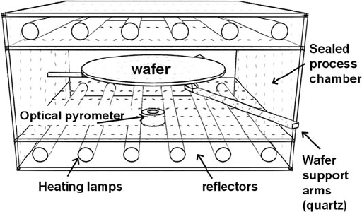
Rapid thermal processes (Fig. 10.38) have been developed as a solution to
the problem of maintaining shallow junction depths while achieving full acti-
vation of high-dose implants [76, 77]. These processes subject a substrate to a
high-temperature anneal for a very short time, measured in minutes or seconds,
and in some of the newest process equipment, milliseconds [78]. The short high-
temperature process allows movement of atoms and dopants over a distance
corresponding to a few lattice constants, enabling removal of crystal damage without
allowing significant diffusion of dopants. Heating is usually applied by high-power
optical lamps that have been carefully arranged to produce very uniform heating of
the substrate. High temperature rate ramping of substrates as brittle as silicon leads
to breakage due to differential thermal expansion if significant thermal gradients are
allowed to form.
Fig. 10.38 Schematic of a rapid thermal processing system processing chamber
As with conventional thermal anneal, the RTP process chamber is often fitted
with a gas injection system allowing oxidation or nitridation of the surface during
anneal [77]. Temperature of the substrate is generally monitored with an optical
pyrometer that controls the lamp intensity in a closed loop system. Severe difficul-
ties can be encountered if the infrared emission characteristics of the substrate are
allowed to vary [76]. This often becomes an issue if there are thin-films of various
types present on the back of the silicon wafer. Often a test wafer fitted with a ther-
mocouple can be used to calibrate the optical pyrometer system for a specific wafer
configuration.

10 Doping Processes for MEMS 803
10.7.3 Low-Temperature Activation
Some process flows r equire a smaller thermal budget than even rapid thermal pro-
cesses are capable of. For example, a process might call for implantation and
activation of a dopant on the back of a wafer that already has a complete device
on the front that will not tolerate temperatures of more than 400
◦
C (a common
CMOS temperature sensitivity), or dopants must be activated in an amorphous
thin-film deposited on a low-temperature glass or polymer substrate. A few rela-
tively exotic processes have been developed to allow activation of dopants at very
low temperatures that are compatible with glass substrates, most metals, and some
polymers.
Excimer and infrared laser annealing processes can be used to activate dopants
after ion implantation on sensitive substrates [79], such as in low-temperature
deposited amorphous silicon on glass used in display applications. These processes
generally work by illuminating a small spot on the substrate with a high-intensity
laser pulse sufficient to liquefy the material [80]. The pulse is of a short duration,
so the melted region quickly resolidifies without significantly heating the bulk of
the substrate, regenerating the crystal structure and providing for some degree of
dopant activation. The pulsed laser beam is scanned across the area to be annealed
by a rastering system. These systems have the advantage of being simple to scale
up to large substrates, making them attractive in a variety of large area display and
solar panel applications [81].
10.7.4 Process Selection Guide: Dopant Activation
Conventional thermal anneal
Thermal budget • Conventional diffusion furnace technology with quartz liners is good up to
1100
◦
C. Silicon carbide tubes are usable to 1200
◦
C. Higher temperatures
require specialized equipment.
Time • Depends on desired diffusion distances and/or degree of crystal damage, but
usually >1 h due to need to ramp furnace temperature.
• Furnace temperature ramp up and down can only be done slowly
(<10
◦
C/min), increasing process time
Material
compatibility
• Silicon
• SiO
2
• Si
3
N
4
• Some refractory metals/silicides
• Materials must have low vapor pressure at process temperature
• Materials must not chemically react or form eutectic alloys with adjacent
materials
• Materials must not have large differences in thermal expansion coefficients
Disadvantages • High temperature
• Lengthy process
