Ghodssi R., Lin P., MEMS Materials and Processes Handbook
Подождите немного. Документ загружается.


774 A.D. Raisanen
Thermal budget Activation of doped regions will generally require anneal or diffusion
temperatures >900
◦
C. Te mperature-sensitive components can be fabricated
on the wafer once the dopants have been activated, but will need to be
protected from t he etch solution by passivation layers or fixturing.
Selectivity Selectivity between n and p silicon-doped regions is reported at 200:1 in KOH
[43] and as high as 3000:1 in EDP [31].
Viable etchants KOH, EDP, and TMAH all exhibit this effect.
Material
compatibility
Same general materials requirements as the underlying KOH, EDP, and TMAH
etch solution. Good electrical contacts must be made to the n-doped layer,
and these contacts must be protected from the etchant.
10.3 In Situ Doping
One of the most effective methods of doping a semiconductor material is during the
growth of that material. Incorporation of dopant atoms during the high-temperature
growth phase results in an undamaged crystal structure with activated dopants,
avoiding the need for subsequent annealing processes and large thermal budgets.
Unfortunately, only bulk material or blanket films can be easily formed in this man-
ner, so complex device structures will generally require some additional processing
technique.
10.3.1 Chemical Vapor Deposition
Polysilicon is a polycrystalline form of silicon commonly used as a thin-film
mechanical material in MEMS and as an electronic gate for MOS electronic devices.
Polysilicon is straightforward to deposit on a wafer surface with chemical vapor
deposition techniques, and is easily etched with a variety of wet chemical and dry
plasma processes. It is compatible with high temperatures, thermally matched to the
underlying silicon wafer, and can be doped to achieve a wide range of conductivity
values.
As stated above, polysilicon is typically deposited using a chemical vapor depo-
sition process in a low-pressure three-zone tube furnace, although the process is also
compatible with single-wafer deposition equipment such as used in cluster tools. A
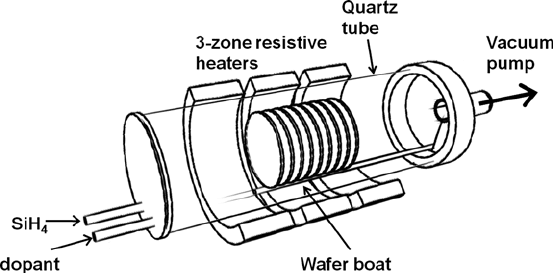
common arrangement is illustrated in Fig. 10.16. Wafers stored vertically in a car-
rier are centered in a three-zone quartz hot wall furnace that is evacuated with a
vacuum pump. A throttle valve controlled by a pressure sensor is normally placed
at the output port to allow continuous closed loop control of the process pressure.
Reactants are introduced at the front of the tube. Silane (SiH
4
) is the most com-
mon reactant gas, but dichlorosilane (SiH
2
Cl
2
) and silicon tetrachloride (SiCl
4
)are
occasionally used as well. At the wafer surface, silane is broken down to produce
elemental silicon and hydrogen gas.
Minor process details, such as reactor vacuum integrity, carbon and oxygen
contamination, and wafer fixturing details can produce significant variations in
10 Doping Processes for MEMS 775
Fig. 10.16 Schematic of low-pressure chemical vapor deposition system
deposition rate and morphology [7], making quantitative comparison of literature
results difficult. A typical undoped polysilicon process r ecipe used in the author’s
laboratory uses a deposition temperature of 650
◦
C, with 100 sccm SiH
4
flow at 300
mTorr total pressure, which produces deposition rates of 110 Å/min. Thickness uni-
formities for a 5000 Å film of <5% within wafer and 10% along the length of the
boat are typical. Three to four sacrificial “dummy” wafers are placed at the front
and back of the boat to improve the thickness uniformity of the device wafers.
A small temperature gradient of 10–15
◦
C is generally added to each zone, with
the coolest zone closest to the gas inlet, and the hottest zone closest to the exhaust
port. The increase in reaction rate at higher temperatures along the wafer load helps
compensate for the reduction in SiH
4
partial pressure at the wafer surface as reactant
is consumed. Increasing silane gas flow or pressure will increase the deposition rate
to some degree, but altering these parameters will also modify the uniformity within
the boat and within each wafer, so it is usually necessary to optimize temperature,
pressure, and gas flow simultaneously to produce a viable process in each individual
reactor.
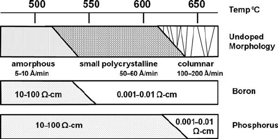
Polysilicon film morphology and deposition rate depend strongly on deposition
temperature, with deposition temperatures below 575
◦
C producing fine-grained or
amorphous films and low deposition rates. Deposition temperatures above 625
◦
C
produce large column-shaped crystallites [44]. Intermediate temperatures produce
small microcrystallites or amorphous films, depending on reactor configuration,
impurities, and other details. Figure 10.17 illustrates the typical morphologies
observed in most reactors, with the transition between amorphous low-temperature
depositions and columnar crystallite depositions occurring gradually somewhere
between 525 and 625
◦
C.
As long as sufficient silane is delivered to the process, deposition rates follow
an Arrhenius relationship with an activation energy of about 1.7 eV [7]. The pro-
cess is then driven by the reaction rate at the wafer surface rather than by mass
transport effects, and good thickness uniformity can be maintained over all wafers.
776 A.D. Raisanen
Fig. 10.17 Polysilicon undoped morphology and in situ doping resistivity trends as a function
of deposition temperature. Minimum resistivities generally observed for high doping densities are
listed for in situ boron and phosphorus-doped films
Lower silane flows result in the deposition process being governed by mass trans-
port rates, and deposition rate, uniformity, and morphology then tend to be much
more sensitive to reactor geometry details.
By adding a suitable source gas to the input reactant stream during chemi-
cal vapor deposition, it is practical to dope the polysilicon grains during growth.
Phosphorus oxychloride (POCl
3
) is a liquid material that can be added to the reac-
tor using an inert gas bubbler or vapor draw system, and is used as a phosphorus
dopant in CVD systems. Diborane (B
2
H
6
), arsine (AsH
3
), and phosphine (PH
3
)are
gaseous materials that can be added to the reactor to provide boron, arsenic, and
phosphorus dopants, respectively. Typical dopant flows are no more than a few per-
cent of the silane flow, and using a dilute (e.g., 2% PH
3
in N
2
) s ource gas is not
uncommon for safety reasons [45].
It should be noted that every one of these materials (SiH
4
,POCl
3
,B
2
H
6
,AsH
3
,
and PH
3
) is significantly hazardous, with SiH
4
being pyrophoric, POCl
3
being cor-
rosive, and the rest being very toxic. Safety equipment including gas detectors and
waste scrubbers are critical for these processes. Most workers use in situ doped
polysilicon processes when a heavily doped polysilicon film is desired, such as
that used for comb drives, local interconnect, gates, and other electrostatic devices.
Resistance control of in situ doped material for lighter-doping levels tends to be
poor between wafers and from run to run, often making simpler diffusion or ion
implant processes more attractive for these applications.
At low doping levels, dopants tend to segregate to the grain boundaries between
crystallites, producing little effect on the conductivity of the polycrystalline film.
Resistivity of polysilicon at low dopant levels is then very sensitive to the exact mor-
phology of the film. Dopants added to amorphous films collect at the large numbers
of grain boundaries between the numerous small crystallites, where they are rela-
tively ineffective compared to the same dopant density added to more crystalline
films grown at higher temperature, where more of the dopant is incorporated in the
10 Doping Processes for MEMS 777
crystallites themselves. This leads to a relatively abrupt decrease in the resistivity
observed for a polysilicon film saturated by dopants as the morphology of the film
goes from amorphous to columnar crystalline at increased deposition temperatures.
Addition of phosphorus (PH
3
) dopant during the polysilicon deposition pro-
cess has the effect of suppressing large crystallite growth until higher temperatures
are achieved relative to an undoped deposition, as illustrated schematically in
Fig. 10.17. The minimum r esistivity achievable tends to be in the range 10–
100 cm below about 625
◦
C, which corresponds to the range where amorphous
deposition occurs. At temperatures higher than about 625
◦
C, the columnar growth
mode predominates, and the minimum resistivity obtainable drops to about 0.001–
0.01 cm. Total deposition rates of polysilicon grown with phosphine and arsine
dopant gases are strongly suppressed [7, 46], with up to an order of magnitude
decrease in deposition rate observed with dopant flows of more than a few percent
of the silane flow.
Addition of boron (B
2
H
6
) dopant during the polysilicon deposition process
increases the deposition rate of polysilicon by as much as two to three times [46],
with little effect on the overall morphology. Low-resistivity polysilicon with large
microcrystallites can be obtained at temperatures as low as 525–550
◦
C.
10.3.2 Crystal Growth and Epitaxy
Conventional crystal growth techniques are used to produce boules and wafers of a
given desired dopant concentration. A wide range of dopant concentrations is pos-
sible but only bulk material can be produced. Much of the silicon produced in the
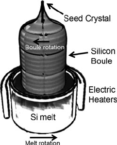
world today is grown by the Czochralski technique illustrated in Fig. 10.18 [47, 48].
A quartz crucible containing very high-purity polysilicon and dopant materials such
as antimony or phosphorus is heated by a set of electric heaters until it is above the
melting point of silicon at 1414
◦
C. A small single-crystal seed of silicon is lowered
into the melt on a support rod, and then slowly withdrawn. The crystal orientation
of the boule can be selected by proper orientation of the seed crystal.
Fig. 10.18 Czochralski
silicon crystal growth method
778 A.D. Raisanen
New silicon grows on the seed from the melt, using the seed crystal structure
as a template, and cools as the boule is withdrawn. The crucible and the growing
boule of single-crystal silicon are continuously rotated in opposite directions as the
crystal is drawn. The entire apparatus is housed in an inert gas environment during
the process, which takes many hours depending on the size of the crystal boule being
grown.
This growth technique produces silicon of a doping level set by the amount of
dopant material included in the original melt. Oxygen, from crucible quartz dis-
solved into the melt by the molten silicon, and carbon, from sublimation of the
carbon heater elements used to heat the melt, are incorporated in the boule dur-
ing growth [48], with typical levels >10
17
cm
−3
for oxygen and >10
15
cm
−3
for
carbon. These impurities are often beneficial in trapping and immobilizing trace
metallic impurities, but can also cause problems for some devices. For example,
oxygen precipitates in silicon used for anisotropic KOH etching can induce small
pitting defects that degrade the mirror finish of etch facets.
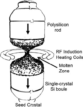
An alternative popular silicon crystal growth method is the float-zone technique
schematically illustrated in Fig. 10.19. This method avoids use of a crucible or other
container that can introduce contaminants into the boule. A large polysilicon rod is
lowered gradually through a zone heated inductively by radio frequency energy. A
seed crystal at the lower end provides the template for single-crystal growth of the
larger boule. Silicon is melted by the RF power, and surface tension of the liquid
allows it to flow down through the hot zone and recrystallize on the seed crystal.
Impurities in the initial polysilicon rod tend to stay segregated in the liquid zone
rather than incorporate in the growing single-crystal zone, so boules of extremely
high purity can be grown this way. Dopants may be introduced by incorporating
them in the original polysilicon rod, exposing the hot zone to a flow of suitable
dopant gas such as phosphine or diborane, or even by feeding a rod of dopant mate-
rial into the molten zone and letting it melt [49]. Silicon with resistivities exceeding
Fig. 10.19 Silicon
single-crystal growth by the
float-zone technique
10 Doping Processes for MEMS 779
10
4
-cm can be grown by this method for special applications such as radio
frequency integrated circuits, which require very low substrate conductivities.
Single-crystal epitaxial films of silicon or other semiconductors are often grown
on wafers that have been prepared by bulk silicon growth techniques such as the
Czochralski or float-zone techniques. Unlike the polycrystalline or amorphous mate-
rials grown with simple polysilicon deposition methods, these epitaxial growth
techniques replicate the crystal structure of the underlying wafer, producing a thin
layer of single-crystal material with optimized properties. Epitaxial techniques are
widely used to grow semiconductor layers with specific dopant levels, stacks of
layers with different composition or dopant levels (multilayers), and atomically
abrupt junctions not obtainable with ex situ doping techniques. Alloys such as SiGe
and compound semiconductors can be grown on substrates with the proper lattice
structure using heteroepitaxial growth methods.
A variety of epitaxial growth techniques exists such as liquid phase epitaxy, vapor
phase epitaxy (VPE), molecular beam epitaxy (MBE), atomic layer epitaxy (ALE),
and metal–organic vapor phase epitaxy (MOCVD or OMVPE). Most techniques
operate by heating a substrate to a large fraction of its melting temperature and
exposing i t to a flow of reactants. High substrate temperatures allow for a high
mobility of adatoms on the surface, allowing deposited materials to conform to the
underlying crystal structure.
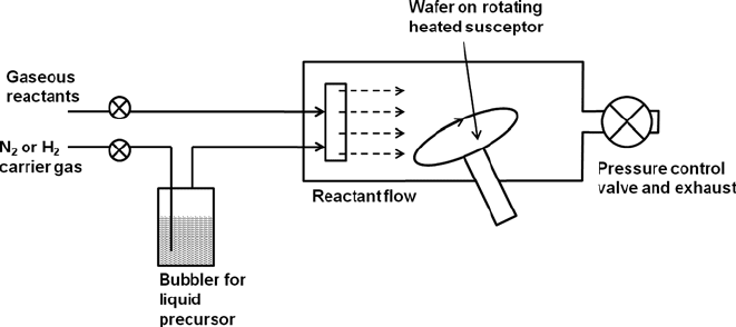
Vapor phase and metal–organic vapor phase epitaxial reactors are probably the
most common systems used for producing commercial quantities of material, as
these systems can achieve a fairly high throughput. See Fig. 10.20. Substrates
may be heated by simple electrical heating elements, optical, or radio frequency
energy, and the chamber walls are generally cooled (“cold wall” reactor), which
minimizes deposition on the walls. Horizontal and vertical configurations exist,
with some reactors accepting one wafer at a time, and others handling multiple
wafers. Subatmospheric pressure processes are typical, but full atmospheric pressure
processes are not unknown.
Fig. 10.20 Metal–organic vapor phase epitaxy (MOCVD) system schematic
780 A.D. Raisanen
A common configuration in the microelectronics industry is the silicon epitax-
ial reactor, which flows hydrogen and silane, dichlorosilane, or silicon tetrachloride
over multiple wafers at temperatures above 900
◦
C. Deposition kinetics is a com-
plex interaction between deposition of Si and etching from the Cl species in the
gas stream. Dopants may be introduced by adding phosphine or other dopant gases.
This produces a high-quality single-crystal film at deposition rates that can approach
1 μm/min. This type of reactor would be used to place a low doping density sil-
icon epilayer over a heavily doped boron etch stop layer, for example, to allow
subsequent fabrication of transistors or other active devices on top of a released
diaphragm.
III-V epilayers for optoelectronic devices are commonly grown using liquid pre-
cursor materials delivered by bubbling hydrogen through a heated fluid bath. Vapor
is entrained in the gas flow and delivered to the reactor. Examples of common liq-
uid precursors for GaAs epitaxy include trimethylgallium (Ga(CH
3
)
3
) and tertiary
butyl arsine AsH
2
(t-C
4
H
9
), but a vast array of chemicals exists for aluminum, gal-
lium, arsenic, phosphorus, and boron sources for MOCVD growth. II-VI materials
such as Hg
1−x
Cd
x
Te, used in infrared detector devices, can also be profitably grown
using MOCVD epitaxy techniques.
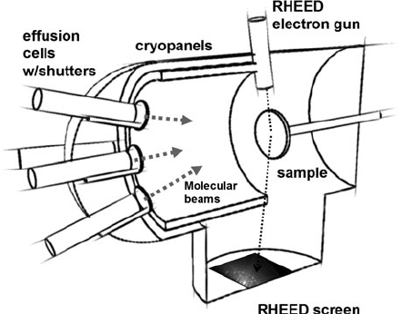
Molecular beam epitaxy (MBE) is a high vacuum deposition technique that
grows an epilayer on a substrate by exposing it to an atomic or molecular beam
of reactant. See Fig. 10.21. For example, elemental Si is used for deposition of Si
epilayers, and Al, Ga, and As are used to deposit Al
1−x
Ga
x
As alloy semiconduc-
tor epilayers. Beams of dopant atoms can also be added to the flux of material
impinging on the substrate, allowing very precise control of dopant level and
alloy composition. Beams of solid-source material are generated by temperature-
controlled collimated evaporation cells (“effusion” or “Knudsen” cells) equipped
Fig. 10.21 Molecular beam epitaxy (MBE) system
10 Doping Processes for MEMS 781
with shutters to start and stop the molecular beam, and liquid and gaseous species
are introduced by special cracking cells or gas injectors.
Deposition rates are generally low, on the order of 1 μm/h or less. The vacuum
system is maintained at a low pressure (10
−7
−10
−11
torr) ensuring that chemical
reactions only occur at the substrate when the beams impinge on it, and to prevent
contaminants from being included in the growing film. Large vacuum pumps and
liquid nitrogen cooled cryoshrouds help maintain low pressure and adsorb stray
gas molecules before they can be incorporated in the epilayer. Most MBE systems
can only deposit an epilayer on a single substrate at a time. This, coupled with the
low deposition rate, makes the MBE growth technique less popular for production
of commercial quantities of epitaxial material, but they are capable of producing
very precise structures with material composition and doping density modulated
at the monolayer level, which is often not practical with MOCVD or other high-
throughput techniques.
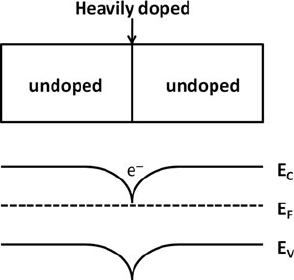
For example, “delta doping” (Fig. 10.22) is a technique used to produce an
extremely abrupt layer of dopants with very high dopant levels [50] that can actu-
ally exceed the solid solubility limits in bulk material. The dopants are confined to
a narrow region of material, often as thin as a single atomic layer in the crystal.
This thin dopant layer alters the electronic structure of the semiconductor, forming
a narrow, deep quantum well in the conduction band that can trap electrons in the
form of a highly mobile two-dimensional “electron gas.” If the well is sufficiently
deep and narrow, a set of electronic subbands is also formed which have unique
optical and electronic properties. High-performance transistors can be fabricated by
this approach which takes advantage of the high mobile charge density in the con-
duction channel and resonant tunneling effects. Optical devices such as lasers and
detectors are also made possible by transitions between the well subbands.
Fig. 10.22 Delta doping
concept. A layer of very
heavy dopant density is
grown between two layers of
much lighter dopant density.
Conduction and valence
bands form a potential well
that can confine electrons in a
two-dimensional layer
10.4 Diffusion
Diffusion processes to fully dope a thin-film or produce a desired dopant pro-
file are common in the semiconductor and MEMS fields. These processes rely on

782 A.D. Raisanen
straightforward thermal diffusion of dopant species from areas of high concentra-
tion to areas of low concentration at high temperature, usually >900
◦
C in silicon
materials.
Diffusion of dopants in Si and other materials can be described by Fick’s law
of diffusion [50], where the concentration of dopant at time t and depth x below a
surface is usually expressed in simplified form as
∂C(x, t)
∂t
= D
∂
2
C(x, t)
∂x
2
, (10.2)
where D (in cm
2
/s) is the diffusivity of the dopant species in Si at a specified tem-
perature. More advanced models incorporate the fact that this diffusivity is actually
a function of dopant concentration and is affected by other factors such as oxidizing
or nitridizing ambient environments in the diffusion tube, but for reasonably low
concentrations and inert environments it can be regarded as a constant.
In the simplest possible model, diffusivity varies with temperature according to
an Arrhenius relationship,
D = D
0
exp
−
E
a
kT
, (10.3)
where D
0
is the frequency factor and E
a
the activation energy for diffusion. More
complex models for D
0
incorporate corrections for concentration, crystal damage,
oxidation, and other factors [52, 53]. Values for D
0
and E
a
for a few typical silicon
dopants in single-crystal silicon are given in Table 10.1. Diffusivity will depend on
the concentration of interstitials, vacancies, grain boundaries, and other defects in
the crystal [54, 55], so it is clear that polycrystalline material will have a significantly
higher diffusivity than single-crystal materials.
Table 10.1 illustrates that the diffusion constant for As in polysilicon is more
than 10
3
higher than in single-crystal silicon even at relatively low temperatures.
Diffusion through polysilicon films is strongly influenced by the morphology of
the film, but because the diffusivities are high and the film thicknesses are low, in
practice even a short anneal will evenly distribute any dopant evenly throughout the
thickness of the film. Lateral diffusion of a micron or more can be expected with
polysilicon even during short high-temperature anneals.
Table 10.1 Frequency factor D
0
and activation energy E
a
for calculating diffusion constants as
a function of temperature (Kelvin) for common dopants in Si. Values for single crystal (c-Si) and
polysilicon (poly) are listed
Dopant D
0
(cm
2
/s) E
a
(eV) Ref
B (c-Si) 2.64 3.6 900–1200
◦
C [Mathiot]
As (c-Si) 35.3 4.11 950–1150
◦
C [Ishikawa]
P (c-Si) 3.62 3.61 950–1150
◦
C [Ishikawa]
As (poly) 8.6 × 10
4
3.9 800
◦
C [Swaminathan]

10 Doping Processes for MEMS 783
Two solutions for Equation (10.2) are broadly useful, corresponding to the case
of (1) constant dopant concentration, and (2) fixed total dopant quantity. Case 1 is
commonly encountered in gas and solid-state diffusion processes where the dopant
is continuously introduced during the process or is available from a large reservoir,
so the dopant is never depleted by the quantity that diffuses into the silicon surface.
The solution that satisfies (Equation (10.2)) under these conditions is
C(x, t) = C
S
erfc
x
2
√
Dt
, (10.4)
where x is the depth below the silicon surface in cm, C
S
is the fixed dopant concen-
tration in the ambient (atoms/cm
−3
), D is the diffusivity from Equation (10.3), and t
is the amount of time that the sample is held at the diffusion temperature in seconds.
The erfc is the complementary error function, which is tabulated in many reference
works [56] and is even a native function supported in spreadsheet applications such
as Microsoft Excel©.
The second case is appropriate for instances where the total amount of dopant at
the start of the diffusion process is fixed at some value and not replenished as it is
consumed by diffusion into the silicon. This is common f or materials such as spin-on
dopants or deposited glass thin-film dopants, which have a finite amount of dopant
in a small reservoir. The solution to Equation (10.2) under this set of conditions is
then given as
C(x, t) =
Q
T
√
πDt
exp
−
x
2
4Dt
, (10.5)
where Q
T
is the total quantity of dopant at the beginning of the anneal at the surface
in atoms/cm
2
.
10.4.1 Gas Phase Diffusion
Gas phase diffusion processes were widely used at the beginning of semiconductor
technology, but tend to be less popular now simply due to the toxic gases required.
Dopant atoms are introduced by flowing a suitable gas such as phosphine, diborane,
POCl
3
, or BCL
3
into a furnace that maintains the substrates at a temperature suffi-
cient to produce indiffusion. See Fig. 10.23. The constant gas flow sets a constant
dopant concentration in t he tube ambient, providing appropriate conditions for the
application of Equation (10.4). A burn box or scrubber of some type is required
for dealing with the toxic effluent from the tube, and the furnace must be sealed or
otherwise isolated from the laboratory environment to prevent even ppm levels of
dopant gas from escaping. Nitrogen or argon is usually admitted to the furnace to
provide an inert environment.
