Ghodssi R., Lin P., MEMS Materials and Processes Handbook
Подождите немного. Документ загружается.

This is Blank Page Integra xxxii

Chapter 10
Doping Processes for MEMS
Alan D. Raisanen
Abstract Doping processes are utilized to modify electrical properties of semi-
conductors by making mobile charge carriers available in the material. Doping
processes are used in MEMS devices for creating electrically conductive layers for
power distribution, heaters, transducers, and other structures. Doped layers are also
widely used for controlling specialty etch processes by modification of surface elec-
trochemistry. Typical MEMS doping applications, s tandard processes for doping
MEMS materials, and diagnostic techniques are reviewed.
10.1 Overview
The doping of semiconductors is one of the oldest and most fundamental processes
used in making semiconductor devices. Doping processes alter the concentration
and distribution of free carriers in a semiconductor matrix, making possible elec-
tronic devices based on p−n junctions or metal–oxide–semiconductor structures.
Doping processes are also critical for the successful formation of electrical con-
tacts in devices fabricated from semiconductors, not only for transistors and other
electronic systems but also for MEMS devices based on silicon or other materials.
The scientific literature related to doping processes for electronic devices is quite
extensive, describing details of dopant distribution and electrical activation impor-
tant in forming ever-shallower dopant profiles for devices at smaller length scales.
In contrast, the role of doping processes in current MEMS fabrication is relatively
straightforward and primarily affects creation of electrically conductive layers and
layers modified to alter material etch properties.
Doped MEMS structures are most heavily utilized as resistive structures for
heaters in thermally driven actuator devices, as heaters in microchemical reactors, or
as piezoresistors in sensor devices. More indirectly, doping processes can be utilized
A.D. Raisanen (B)
IT Collaboratory, Rochester Institute of Technology, Rochester, NY, USA
e-mail: adremc@rit.edu
755
R. Ghodssi, P. Lin (eds.), MEMS Materials and Processes Handbook,
MEMS Reference Shelf, DOI 10.1007/978-0-387-47318-5_10,
C
Springer Science+Business Media, LLC 2011
756 A.D. Raisanen
in sophisticated fabrication techniques utilizing differential etch rates between vol-
umes of silicon doped by different dopant species or concentrations. Most of
discussion here is limited to silicon applications as much of MEMS work to
date is focused on silicon, but all the concepts are generally applicable to other
semiconductor materials.
10.2 Applications
10.2.1 Electrical Properties
Doping is primarily a means of altering the electronic properties of semiconduc-
tors by introducing impurities that contribute free carriers (electrons and holes).
Intrinsic (undoped) semiconductor crystals will contain a modest concentration of
carriers due to simple thermal excitation and defects. This intrinsic carrier den-
sity depends on the semiconductor energy gap and on the temperature [1]. Intrinsic
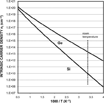
carrier concentration increases exponentially with temperature as illustrated for Ge
and Si single crystals in Fig. 10.1. Unfortunately, at reasonable temperatures these
relatively low intrinsic carrier concentrations are insufficient for most technolog-
ically interesting purposes such as p–n junctions and etch modification, and the
large variation in carrier concentration observed as a function of temperature lim-
its the ability to design devices that operate reliably over a significant temperature
range. Impurity atom dopants can be added to the crystal to overcome these defi-
ciencies. Still, thermal excitation of intrinsic carriers can become important for
semiconductor devices that reach a high temperature, such as heater elements [2]. At
a certain point, intrinsic carrier excitation becomes large enough that it can initiate
Fig. 10.1 Intrinsic carrier
concentration in undoped Si
and Ge crystals as a function
of temperature (Calculated
from models in [1])
10 Doping Processes for MEMS 757
a thermal runaway event, with large currents producing high temperatures, which
excite higher intrinsic carrier densities enabling even higher currents, and eventual
catastrophic results for the device.
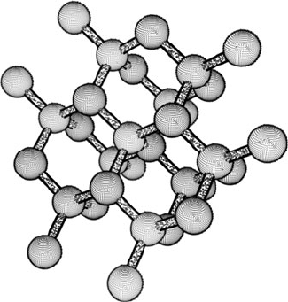
Silicon single crystals have a diamond lattice structure illustrated in Fig. 10.2,
with an underlying face-centered cubic structure and tetrahedrally bonded Si
atoms. Many other technically important semiconductors have a similar diamond
or zincblende structure, such as Ge, GaAs, or β-SiC [3]. In order for impurity atoms
to function as electrically active dopants in the silicon structure, they must be capa-
ble of contributing a mobile electron or hole without acting as an electronic trap
or recombination center [4]. For Si crystals, viable doping impurities are primarily
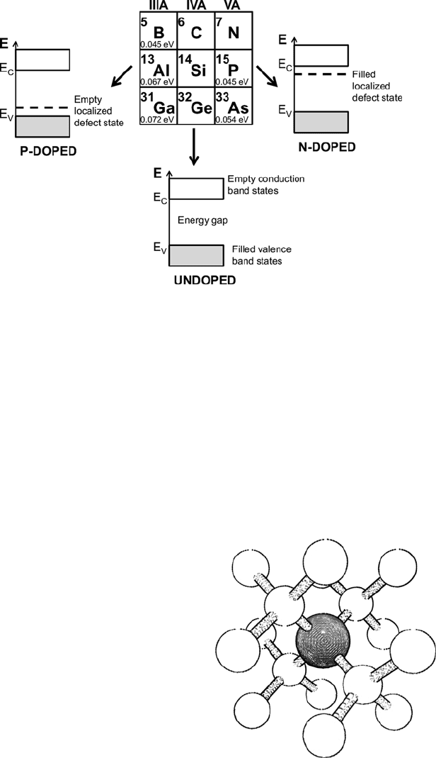
found in either group III or group V of the periodic table (Fig. 10.3).
Group III atoms such as boron, aluminum, and gallium, when incorporated into
the silicon semiconductor lattice, form an empty localized electronic state in the
semiconductor bandgap located just above the valence band edge. Electrons in the
valence band are easily promoted into this state at moderate temperatures, resulting
in a nonlocalized, mobile hole state in the valence band. This hole then acts as a
free carrier in the semiconductor crystal, allowing it to support a current flow. These
group III dopants are known as electron acceptors, and a silicon crystal with an
excess of acceptor levels is defined as p-type.
Group V atoms such as phosphorus, antimony, and arsenic also form localized
electronic states in the silicon bandgap, but these impurities form filled states just
below the conduction band edge. At moderate temperatures, electrons occupying
these states are easily promoted into the conduction band of the semiconductor,
where they act as free electronic carriers. These dopants are known as electron
donors, and a crystal with an excess of donor levels is defined as n-type. It is possible
for a semiconductor crystal to be doped with both donor- and acceptor-type dopants
simultaneously. The donors and acceptors then effectively cancel each other out
(compensation), and the crystal type is essentially determined by which dopant type
predominates.
Fig. 10.2 Atomic
arrangement of a silicon
crystal illustrating the
diamond lattice structure
758 A.D. Raisanen
Fig. 10.3 Portion of the periodic table showing group IV semiconductors and some dopants
important for silicon technologies. Schematic band structures of the silicon crystal are shown
for p-doped (group III impurity), undoped, and n-doped (group V impurity). Energy shown in
electron volts corresponds to the separation between the acceptor state and valence band edge
(p-dopants), or between the donor state and the conduction band edge (n-dopants) (Ionization
energy data from [5])
Impurity atoms added to the crystal can occupy a variety of locations includ-
ing individual interstitial sites between silicon atoms, agglomerated as clusters of
impurity atoms, or at lattice sites replacing a silicon atom. Missing atoms, dis-
placed atoms, dislocations, and other crystal imperfections are also present in any
real semiconductor, and many of these defects can have a significant effect on the
semiconductor electronic structure [6]. See Fig. 10.4. Although many of these point
Fig. 10.4 Dopant atom
incorporation in a silicon
lattice as a substitutional
impurity
10 Doping Processes for MEMS 759
and extended defect structures can act as dopants in a semiconductor, they are gen-
erally very difficult to control from an engineering standpoint. Reproducible devices
are generally made by controlled introduction of substitutional defects. In order to
be electrically active and contribute to the conductivity of the silicon crystal, the
dopant atom must be incorporated into the s ilicon lattice as a substitutional impurity.
Impurity atoms residing in other sites can act as scattering or recombination cen-
ters, degrading carrier mobility without adding to free carrier concentration. Silicon
atoms displaced from lattice sites can also add states in the bandgap, acting as
dopants or scattering centers. These self-interstitial dopants can become important
in ion implant processes or other processes that cause silicon crystal damage.
The most commonly used dopants in silicon include B as an acceptor and P,
As, and Sb as donors. These dopants are chosen for ease of processing, high solid
solubility, and controllable diffusion characteristics. Dopants may be introduced into
the crystal during growth or deposition, or introduced externally by diffusion or ion
implantation [7]. It is a straightforward exercise to adjust the dopant concentration
in the crystal to obtain a desired material resistivity through a very broad range, for
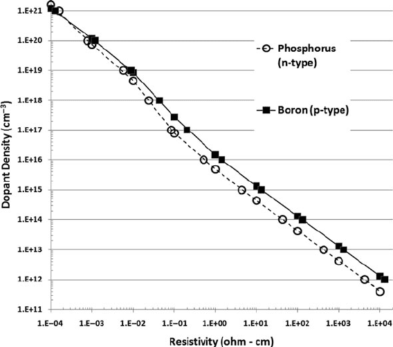
applications like silicon-based resistors or heater elements. Figure 10.5 illustrates
the relationship of silicon crystal resistivity to carrier concentration for phosphorus
(n-type, donor) and boron (p-type, acceptor) impurity atoms at 300 K.
Fig. 10.5 Resistivity of boron and phosphorus doped silicon as a function of dopant concentration
at 300 K (Data tabulated in [8])
760 A.D. Raisanen
The total amount of dopant which may be loaded into a silicon crystal is limited
by the solid solubility of the impurity atom in the silicon lattice. If a higher dopant
concentration is attempted, additional dopant atoms will fail to incorporate in the
silicon lattice, instead segregating into inclusions or clusters of dopant atoms that
do not contribute to the crystal’s carrier concentration, and may in fact degrade the
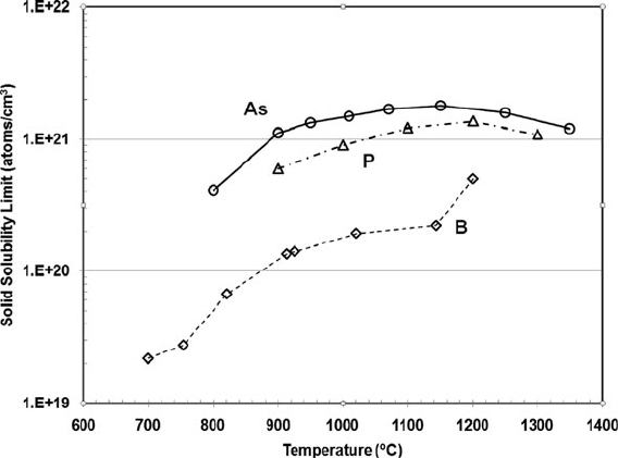
conductivity of the crystal by trapping or scattering mobile carriers. Figure 10.6
illustrates the measured solid solubilities of different species in silicon as a function
of temperature [9–11]. Standard silicon dopants such as B, As, and P have quite high
solid solubility, making it possible to very heavily load silicon with active dopants
to obtain high electrical conductivities.
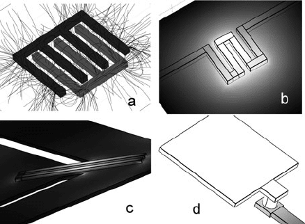
In MEMS technologies, one of the key applications of doping technology is fabri-
cation of conductors and resistors in silicon, as schematically illustrated in Fig. 10.7.
These structures are easy to integrate into a variety of silicon processing schemes in
both bulk and surface micromachining processes. Silicon conductors and resistors
require high-temperature processing to implement but will also tolerate very high
temperatures without damage, making them ideal for process sequences involving
anneals for stress relief, thermal oxidation, or other high-temperature processes.
In addition to being utilized as gate electrodes in MOS devices and as general
interconnect “wiring” on a chip [7], heavily doped silicon layers are commonly
used as electrically conductive structural elements. These materials find use in elec-
trostatically driven devices such as comb drives [12], which benefit from the highest
conductivity, and thus highest active doping density, obtainable. Single-crystal
Fig. 10.6 Solid solubility of important dopants in Si as a function of temperature (Boron from
Vick [9] and Trumbore [10], phosphorus from Trumbore [10], and arsenic from Trumbore [10]
and Sandhu [11]. Used with permission)
10 Doping Processes for MEMS 761
Fig. 10.7 Archetypical applications of doped Si structures in MEMS: (a) electrostatic structure
(comb drive, showing electric field lines), (b) transducer resistive element (electrical heater, show-
ing thermal power dissipation), (c) sensing resistive element (strain gauge on supported diaphragm,
showing Von Mizes stress), and (d) electrical contact to metal pad for input/output
silicon or silicon-on-insulator materials used to fabricate such structures can be
readily obtained with resistivities down to 10
−3
cm or better. Deposited materials
such as polysilicon thin-films will be substantially worse due to lower mobilities
and higher scattering, but even polysilicon is easily doped to resistivities of 0.1
cm, corresponding to sheet resistances of 25 /square for a 500 nm thick layer.
Resistive elements may be fabricated with a very broad range of resistive val-
ues. The greatest advantage of silicon as a resistor material is that the resistivity
may be tuned to match the needs of the application through about seven orders of
magnitude as illustrated in Fig. 10.5. In contrast, most thin-film resistor materials
such as TiW or TaN can only be adjusted through a comparatively narrow range by
altering process conditions such as reactive gas background, pressure, or deposition
temperature [13].
Resistors in MEMS are often used as heater elements to provide motion via dif-
ferential thermal expansion, or as simple heaters to drive chemical reactions. Silicon
resistors also make excellent strain gauge elements for mechanical sensing appli-
cations. The resistance of a resistor is significantly altered by a mechanical stress
applied to the device, according to the piezoresistive coefficient of the resistive mate-
rial. In silicon, the piezoresistive coefficient decreases as the doping level increases.
For maximum sensitivity to mechanical stress, a low doping concentration, and
hence high resistivity, is advantageous.
Figure 10.8 illustrates piezoresistive coefficients for single-crystal silicon at 25
◦
C
in the (100) plane, a common SEMI standard wafer type used in the microelec-
tronics industry. The data are consolidated from data and calculations by Kanda
[14]. Longitudinal coefficients correspond to the case where the mechanical stress
is applied parallel to the current flow in the silicon, and transverse coefficients
correspond to the case where the applied mechanical stress is perpendicular to the
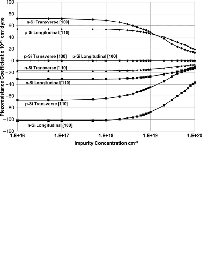
762 A.D. Raisanen
Fig. 10.8 Single-crystal silicon piezoresistive coefficients as a function of active impurity concen-
tration for p-type and n-type material. Transverse coefficients indicate that the tensile stress and
electric current are a t right angles to each other, and longitudinal values indicate that the stress and
electric currents are parallel (Consolidated from calculations by Kanda [14], used with permission)
current flow. Coefficients are shown for resistors oriented in the [100] direction, ori-
ented 45
◦
to the flat on a (100) wafer, or resistors oriented in the [110] direction,
perpendicular or parallel to the (100) wafer flat. These are common resistor con-
figurations for strain sensors on cantilevers or membranes fabricated on a silicon
surface.
The change in resistance of a resistor is then related to the piezoelectric
coefficient by
ρ
ρ
= σ (10.1)
where σ is the applied mechanical stress and is the piezoelectric coefficient in
the appropriate direction. Figure 10.8 clearly implies that resistors oriented in the
[100] direction are best fabricated from n-doped material, whereas resistors in the
[110] direction will have highest sensitivity if fabricated from p-doped material.
Polysilicon is also widely used for piezoresistive sensors despite having typically
lower piezoresistive response compared to single crystal silicon [15], although
the piezoresistive coefficients show considerable variation related to polysilicon
microstructure and fabrication details.
10 Doping Processes for MEMS 763
Silicon is commonly used as a “local interconnect” material in microelectronic
and MEMS devices [7]. Although it has relatively high resistivity relative to metallic
conductors such as aluminum, silicon will tolerate high-temperature processing and
is quite suitable for short electrical leads. Fabricating these local interconnects or
resistors is usually a straightforward process of doping the silicon to a conveniently
high value, annealing it to redistribute and activate the dopants, then patterning and
etching the silicon to produce a well-defined lead or resistor structure.
In order to fully utilize silicon as a conductive material, it is generally neces-
sary to form metal contacts on the surface to allow the connection of wires or
other probes in a packaged device. Gold and aluminum wire bonds to metal pads
are very common interconnect methods, and high-volume applications use solder
bumps formed on the metal pad to enable “flip-chip” and related packaging tech-
niques. For research purposes, making direct contacts to heavily doped silicon with
a metal probe tip is possible, but such simple contacts tend to be mechanically and
electrically unreliable for anything other than short-term usage.
Metal–semiconductor contact formation is a topic that has received heavy inves-
tigation over the decades [16], and continues to receive attention to this day.
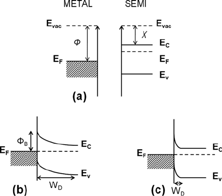
Application of a metal film to a semiconductor surface causes a redistribution of
charge carriers in the near-surface region of the semiconductor as illustrated by the
energy-level diagrams in Fig. 10.9. The metal, shown in Fig. 10.9a on the left, is
Fig. 10.9 Energy band diagrams for metal/n-semiconductor contacts. The metal and semicon-
ductor surfaces are separated in (a), showing the respective Fermi levels, valence and conduction
bands, and vacuum levels. The two surfaces are placed in contact in (b), illustrating the redistribu-
tion of charge which brings the metal and semiconductor Fermi levels into alignment, producing
band bending of the conduction and valence bands in the semiconductor. A Schottky barrier of
height
B
is generated at the interface. In (c), the doping level of the semiconductor is much
higher than in (b), producing a very narrow depletion width W
D
, through which carriers can easily
tunnel
