Ghodssi R., Lin P., MEMS Materials and Processes Handbook
Подождите немного. Документ загружается.


724 D.R. Hines et al.
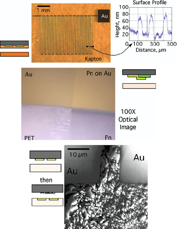
Fig. 9.45 Transfer printed films: (a) Optical image of a Au serpentine line transfer printed onto a
Kapton substrate; (b) optical image of a Pn film (and Au film) printed onto a PET substrate; and
(c) SEM image of a CNT network printed onto a PET substrate. The substrate contains previously
printed Au electrodes (a)and(c). Reprinted by permission from [220]. (b) Reprinted by permission
from [221]
Au to Si is low enough to allow Au to be easily printed onto a plastic substrate (such
as PET or PC). However, the adhesion of Al to Si is too high for the Al print from a
bare Si substrate.
If, however, the Si surface is coated with a TDFS SAM prior to Al deposition,
then the adhesion of the Al to the Si substrate surface can be reduced to the point
where it can be successfully printed. The same is true for PMMA films. Also P3HT
has been shown to print better from OTS-coated Si as compared to bare Si sub-
strates. In addition to lowering the adhesion between the printable layer and the

9 MEMS Lithography and Micromachining Techniques 725
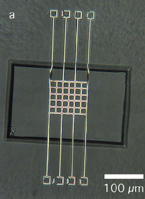
Fig. 9.46 Micrograph
showing a Si grid resonator
printed over a preprinted
cavity on PC film
transfer substrate, the adhesion between the printable layer and the device substrate
can be increased. This can be accomplished in various ways using SAMS [223],
plasma treatments [224], increased surface roughness, and so on. The transfer print-
ing method described above has been implemented to assemble dissimilar materials
sequentially onto a single substrate for the fabrication of both electronic devices
such as thin-film transistors and mechanical devices such as thin-film resonators;
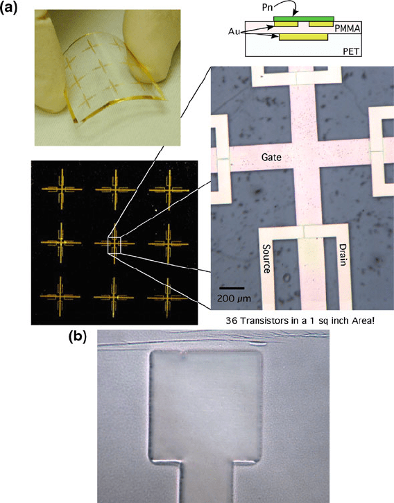
examples of both are shown in Fig. 9.47.
9.7 Case Studies
In a commercial semiconductor device fab or MEMS foundry, the lithography is per-
formed using large-diameter wafers (8–12 in. diameter). The wafers are mounted
in cassettes that can be loaded into each machine or solvent bath for automated
processing. In a research and development lab it is more typical to handle smaller-
diameter wafers (3–6 in.) or even pieces of a wafer such as 1 × 1cm
2
.The
following case studies are geared toward the processing methods in a research and
development lab.
9.7.1 Case Study 1: Substrate Cleaning-RCA Clean(s)
Werner Kern developed the basic procedure in 1965 while working for Radio
Corporation of America (RCA). The full cleaning procedure consists of three steps:

726 D.R. Hines et al.
Fig. 9.47 (a) Electronic and (b) mechanical devices assembled onto plastic substrate using transfer
printing methods (Reprinted by permission from [ 220]and[225]
1. Removal of the organic contaminants (organic clean)
2. Removal of thin oxide layer (oxide strip)
3. Removal of ionic contamination (ionic clean)
9.7.1.1 Recipe Steps
Organics Removal (RCA1)
1. Submerge substrate in a 1:1:5 solution of NH4OH + H
2
O
2
+ H
2
O at 75–80
◦
C
for 15 min.
9 MEMS Lithography and Micromachining Techniques 727
2. Rinse in DI water.
3. Blow dry with N
2
gas.
4. Put in 120
◦
C oven for 20 min.
Oxide Removal (RCA2)
1. Submerge substrate in a 1:50 solution of HF + H
2
O (buffered oxide etch -BOE)
at 25
◦
Cfor1min.
2. Rinse in DI water.
3. Blow dry with N
2
gas.
4. Put in 120
◦
C oven for 20 min.
Ionic Contamination Removal (RCA3)
1. Submerge substrate in a 1:1:6 solution of HCl + H
2
O
2
+ H
2
O at 75–80
◦
Cfor
15 min.
2. Rinse in DI water.
3. Blow dry with N
2
gas.
4. Put in 120
◦
C oven for 20 min.
9.7.1.2 Notes
In many cases, removal of organic contamination is sufficient; however, further
cleaning can be performed for removal of oxide layer and ionic contamination.
9.7.2 Case Study 2: Substrate Cleaning, O
2
Plasma Clean
The O
2
plasma cleaning method is primarily used to remove organic contaminants.
One of the main advantages of plasma cleaning is that it does not employ wet chem-
istry. This case study is based on using a PlasmaTherm 970 Reactive Ion Etcher
(RIE).
9.7.2.1 Recipe Steps
1. Load wafer into the plasma chamber.
2. Run O
2
plasma for 5 min at 200 W, 100 mtorr, 20 SCCM.
3. Vent chamber and remove wafer.
9.7.2.2 Note
Depending on processing conditions, plasma treatments have the potential to affect
the roughness of the substrate surface. Usually the roughness increases.
728 D.R. Hines et al.
9.7.3 Case Study 3: Substrate Cleaning, Solvent Clean
The solvent clean is a general-purpose method that can be performed in most any
laboratory environment.
9.7.3.1 Recipe Steps
1. Submerge a substrate for 5 min in separate beakers of each of the following
solvents.
Trichloroethylene (TCE)
Acetone
Methanol
2-propanol (IPA)
2. Rinse with fresh IPA.
3. Blow dry with dry N
2
gas.
4. Place in 120
◦
C oven for 20 min.
9.7.3.2 Note
As the wafer is transferred from one bath to the next, be sure that the wafer surface
stays wet and that no part is allowed to dry before entering the next bath – never
let the wafer surface dry – always keep the wafer surface wet. For example, acetone
tends to leave a very thin residue on the substrate surface that is extremely difficult
to remove. As an optional step, ultrasonic agitation can be added to each solvent
bath during cleaning.
9.7.4 Case Study 4: Positive Photoresist Processing: General
Processing for Shipley 1800 Series Photoresist
This case study is adapted from processing notes from the Cornell Nanofabrication
Center. Shipley 1800 series photoresist is a general-purpose, broadband (365–
436 nm) positive resist. It is best suited for use on a 5x stepper and HTG Contact
Aligner. It is not recommended for the 10:1 Stepper. The 1800 series resists include
S1805, S1813, S1818, S1818J (dyed), S1827 (0.5, 1.3, 1.8, and 2.7 µm). This case
study assumes that the substrate is a Si wafer.
9.7.4.1 Recipe Steps
1. (Optional) After wafer cleaning, perform a dehydration bake by putting the
substrate in a drying oven at 150
◦
C for 30 min.
2. Mount the substrate onto a spin coater and verify that the spin coater is set up
with the appropriate parameters.
9 MEMS Lithography and Micromachining Techniques 729
3. Apply an HMDS treatment to the substrate surface. Using a disposable pipette,
syringe, or eye-dropper, apply HMDS solution to the entire substrate surface.
Allow to sit for 10 s and then spin for 30 s at 3000–5000 rpm on a spin coater.
4. Dispense photoresist onto the middle of the substrate and spin at the desired
speed for 20–30 s (thicker films take a longer time to reach uniformity). Substrate
surfaces containing topography may benefit from slower rate rates.
5. Soft bake by removing the substrate from the spin coated and placing of a hot
plate. Bake for 1–2 min at 90–115
◦
C. Thicker films benefit from longer baking
times.
6. Mount the photoresist coated substrate and the appropriate photo mask into the
contact aligner (see contact aligner case study) and expose for the desired time.
Exposure time will vary depending on resist thickness, baking time, substrate
reflectivity, and so on.
7. Develop for 1 min in AZ 300MIF or CD 26. Can also use MF-321 (no dilution),
or Microposit Developer Concentrate (MDC) diluted 1:2 (MDC minimizes Al
etch rate but is not metal-ion free). Use agitation while developing.
8. (Optional) Hardbake at 115
◦
C for 1 min on the hot plate, or 20–30 min in the
oven. The hardbake serves to promote adhesion during wet etching or increase
selectivity during dry etching.
This case study is generic with some processing conditions not specifically
stated. Below is a specific case study designed for S1813. Positive photoresists can
be sensitive to humidity. After UV exposure it may be advantageous to leave the
photoresist coated substrate sit out in the cleanroom for 30 min. This allows the
photoresist layer to absorb humidity which tends to minimize the production of
bubbles in the resist layer during postbake.
9.7.5 Case Study 5: Positive Photoresist Processing: Specific
Processing for Shipley S1813
This case study is adapted from the Ph.D. thesis titled “Design of MEMS-
based Tunable Antennas, Organic Transistors, and MEMS-based Organic Control
Circuits” by Madhurima Maddela, Auburn University. The processing steps are
designed specifically for Shipley S1813 positive photoresist.
9.7.5.1 Recipe Steps
1. Clean the substrate.
2. Mount the substrate onto a spin coater and verify that the spin coater is set up
with the appropriate parameters.
3. Dispense enough S1813 photoresist to cover the center half of the substrate and
then spin coat for 30 s at 2500 rpm using a ramp rate of 500 rpm.
730 D.R. Hines et al.
4. Softbake the photoresist coated substrate by placing it on a hot plate at 110
◦
C
for 60 s.
5. Mount the photoresist coated substrate and the desired photo mask into an optical
projection system (i.e., a contact aligner or a stepper) and expose. The exposure
time varies from system to system and will most likely need to be determined by
trial and error. Ask a fellow cleanroom worker or technical support staff member
for a good starting point.
6. Perform a postexposure bake by placing the substrate onto a 110
◦
C hot plate for
60 s.
7. Develop the photoresist layer by submersing in CD-30 photoresist developer for
45 s. Gently agitate while in the solution. Remove the substrate and rinse for 30 s
in DI water. Remove the substrate from the DI water and dry with a N
2
gun.
9.7.6 Case Study 6: Positive Photoresist Processing: Specific
Processing for OiR 906-10
This case study is adapted from the Ph.D. thesis titled “Monolithic Suspended
Optical Waveguides for InP MOEMS” by Kelly, Master’s Thesis, University of
Maryland, College Park, MD, June 2005. The processing steps are designed specif-
ically for OiR 906-10 positive photoresist. In order to achieve optimum sidewall
roughness and angle and the best possible feature resolution, projection lithography
was used to pattern suspended waveguides. A 5x reduction Alphastep 1000 stepper
lithography system was used to achieve critical dimensions down to 0.5 µm. A 5 in.
chrome on quartz mask witha5cm× 5 cm mask area and a 0.1 µm spot size was
used. This 25 cm
2
mask area was stepped down to a 100 mm
2
area on the chip.
9.7.6.1 Recipe Steps
1. Clean the substrate.
2. Mount the substrate onto a spin coater and verify that the spin coater is set up
with the appropriate parameters.
3. Apply an HMDS treatment to the substrate surface. Using a disposable pipette,
syringe, or eye-dropper, apply HMDS solution to the entire substrate surface.
Allow to sit for 10 s and then spin dry for 60 s at 3000 rpm on a spin coater.
4. Dispense enough Arch OiR906-10 photoresist to cover the center half of the
substrate and then spin coat for 60 s at 3000 rpm. The target photoresist film
thickness is 1 µm.
5. Softbake the photoresist coated substrate by placing it on a hot plate at 90
◦
Cfor
60 s.
6. Mount the photoresist coated substrate and the desired photo mask into the step-
per and exposure for the desired time. The stepper parameters and exposure time
may best be determined by first exposing and developing a test wafer (see process
notes below).
9 MEMS Lithography and Micromachining Techniques 731
7. Perform a postexposure bake by placing the substrate onto a 110
◦
C hot plate for
60 s.
8. Develop the photoresist layer by submersing in ODP 4262 photoresist developer
for 60 s. Gently agitate while in the solution. Remove the substrate and rinse for
30 s in DI water. Remove the substrate from the DI water and dry with a N
2
gun.
9.7.6.2 Notes
Several alignment procedures associated with the Alphastep stepper may need to
be carefully addressed: autoleveling of wafer pieces cannot be implemented on this
stepper and the lamp intensity can fluctuate over periods of only a couple of hours.
In order to level the wafer pieces, we employed a technique of shimming the chuck
using various pieces of aluminum foil and Post-It notes. A program was run to
measure the wafer height across the chip using the stepper’s laser measurement
system, then the chuck was shimmed to try to level the surface. The focal depth
of the stepper optics was 2 µm, so this process was repeated until the die-to-die
variation in height was less than 1 µm. In our case, a single 10 × 10-mm die per
chip was used so the entire chip area had to be leveled to ±1 µm to achieve optimum
resolution.
In order to provide the correct exposure time and focus depth, a focus exposure
matrix was used prior to exposing each chip. A mask with a test pattern of bars and
spaces varying from 2.0 µmdownto0.5µm in width was used for this matrix. An
exposure dose between 100 and 120 mJ/cm
2
with a focus depth between −1 and 1
provided the best feature resolutions and resist profiles. The optimum exposure time
and stepper parameters were determined from an optical inspection of the developed
test wafer(s) using a high-quality optical microscope.
9.7.7 Case Study 7: Negative Photoresist Processing: Specific
Processing for NR7-1500PY
This case study describes specific processing conditions for the Futurrex NR7-
1500PY negative photoresist. An MJB3 manual contact aligner is used for UV
exposure.
9.7.7.1 Recipe Steps
1. Perform solvent clean on a Si wafer.
2. Mount wafer on spin coater and set up spin coater with a ramp rate of 1000 rpm
and spin speed of 4000 rpm and a time of 60 s.
3. Dispense photoresist onto the surface of the wafer. Dispense enough resist to
cover at least half the surface area of the wafer. Turn on the spin coater.
4. Remove the photoresist coated substrate from the spin coated and place on a
preheated hotplate at 90
◦
Cfor1min.
732 D.R. Hines et al.
5. Mount the substrate and desired photomask onto the MJB3 contact aligned. With
the microscopy, image a feature on the mask. Then, using the z-translation bar
and fine adjustment knob, raise the wafer up such that the top surface of the
photoresist is just below the bottom surface of the mask when the z-translation
bar is in the “contact” position (be sure that the slide bar is in the contact position
and not in the “soft contact” position). This is the position just before the shadow
image of the mask feature disappears. Using the z-translation fine-adjustment
knob, raise the wafer into contact with the mask. This is the point where the
shadow image of the mask feature disappears. Now move the slide bar into the
soft contact position. At this point the mask and photoresist surfaces will be in
focus but not in contact. Adjust the X, Y, and Rotation of the wafer to be in
alignment with the mask. Once proper alignment has been established, move the
slide bar into contact mode. Set the exposure time to 16 s and push the expose
button.
6. Remove the wafer from the contact aligner and place onto a preheated hotplate
at 90
◦
Cfor1min.
7. Submerge the wafer into a bath of RD6 photoresist developer for 15 s. Gently
agitate either the solvent or the wafer during developing. Remove the wafer and
submerge into a bath of DI water for 30 s and apply agitation. Remove the wafer
from the DI water bath and rinse in DI water (i.e., spray down with a squirt bottle
filled with DI water). Then dry with N
2
gas (i.e., use a N
2
gas stay gun equipped
with a point-of-use filter connected to a clean dry source of N
2
gas).
8. Perform etch or deposition processing as required.
9. Prepare a bath of RR2 photoresist solvent that is large enough so that the wafer
can be vertically submerged (not laying flat but rather standing on edge). Also
prepare separate acetone and IPA baths in which the wafer can lay flat. Place the
RR2 bath on a hotplate and heat the solution to 85
◦
C. Be very careful not to let
the solution temperature rise above 100
◦
C as RR2 is flammable! Place the wafer
vertically into the warm RR2 bath and gently agitate. Once liftoff is complete,
transfer the wafer to the acetone bath. Agitate gently and then transfer the wafer
to the IPA bath (as the wafer is transferred from one bath to the next, be sure that
the wafer surface stays wet and that no part is allowed to dry before entering the
next bath – never let the wafer surface dry – always keep the wafer surface wet).
Remove the wafer from the IPA bath and rinse it down with IPA from a squirt
bottle. Then dry with N
2
gas.
9.7.7.2 Note 1
For liftoff involving Au films less than 100 nm thick, the metal film tends to lift
off in small pieces and look like a fine mesh as it lifts off. Au pieces that are tens
of microns in size tend to backstick to the patterned Au features and cannot be
subsequently removed. This backsticking can largely be prevented by processing
1
/
4
-wafer pieces in a 500 ml bath of RR2 that is stirred at 300 rpm with a 1 in. long
stir bar. The wafer piece is held with flat nose metal tweezers at a position such that

9 MEMS Lithography and Micromachining Techniques 733
the top surface of the wafer is pointed slightly down from the vertical and so that
the backside is slightly turned into the solvent flow. This sample position allows the
Au film and pieces to be swept away from the wafer surface during liftoff.
9.7.7.3 Note 2
Thicker Au films can take several to ten or so minutes to completely lift off. We have
found that the liftoff time can be dramatically reduced by performing an O
2
plasma
exposure after deposition but before liftoff. For example, 5 min in a PlasmaTherm
790 at 200 W, 19 SCCM O
2
, and 100 mtorr reduces the liftoff time from about
10 min to about 1 min for a 100 nm thick Au film. RR2 is an aggressive solvent
and can attack the Si surface; therefore, there can be an advantage to shorter liftoff
times. Albeit with limited investigation, the plasma exposure does not appear to
adversely affect the Au or Si surfaces, such a process may not be compatible with
other materials or with previous processing steps that may have been performed on
the wafer.
9.7.8 Case Study 8: E-Beam Lithography
E-beam lithography can be performed with any number of different SEM systems,
therefore only a generic account of SEM functions is presented as part of this case
study.
1. Start with a 1 cm
2
Si substrate that has been cleaned (see cleaning procedures
for UV lithography).
2. Spin coat a layer of MMA at 4000 rpm for 60 s and bake for 5 min at 200
◦
C.
3. Spin coat a layer of PMMA 950 K A7 at 4000 rpm for 60 s and bake for 5 min
at 180
◦
C.
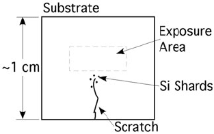
4. With a diamond scribe, scratch a line i nto the PMMA. Go deep enough to pro-
duce a small number of Si shards near the end of the scratch. An example is
shown in Fig. 9.48.
5. Mount the substrate on the SEM sample holder. It is usually a good idea to place
the sample in a specific orientation so that it is easier to locate and align the
Fig. 9.48 Illustration of
substrate for e-beam
lithography
