Ghodssi R., Lin P., MEMS Materials and Processes Handbook
Подождите немного. Документ загружается.

714 D.R. Hines et al.
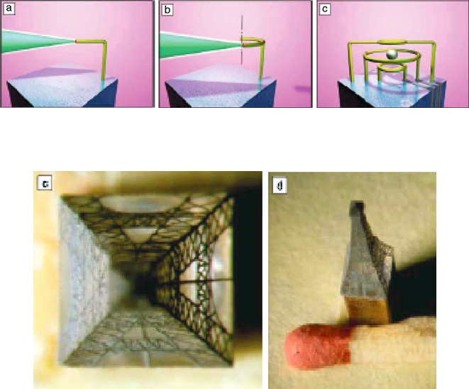
Fig. 9.39 Schematic illustration of LCVD process (Reprinted with permission from [136])
Fig. 9.40 Three mm tall replica of the Eiffel Tower fabricated using LCVD (Reprinted with
permission from [136])
the laser is moved. Figure 9.40 shows a 3 mm tall replica of the Eiffel Tower fabri-
cated using LCVD to deposit Al features onto a preformed polycarbonate structure.
9.5.6 Stereolithography and Microstereolithography
Stereolithography (SL), sometimes referred to as rapid prototyping, was first intro-
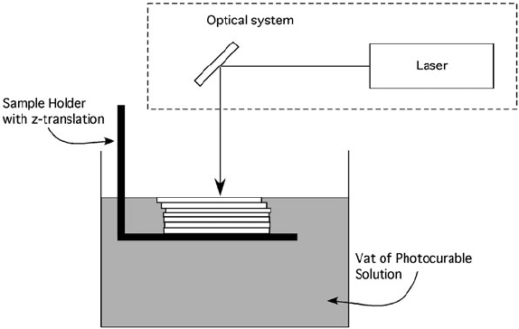
duced in 1981 [137–139]. In its simplest form it employs a laser source, a vat of
photocurable polymer, a sample holder, and a means of moving the beam relative to
the liquid polymer. A CAD-generated design is used to control the relative motion
between the laser and the vat causing photopolymerization where the laser interacts
with the liquid polymer. This mapping/polymerization produces a solid structure
defined by the CAD control and held in place by the sample holder. The process is
shown schematically in Fig. 9.41.
The process can also be performed with solutions loaded with photocurable
metallic or ceramic suspensions. In this way, metal or ceramic parts can be fab-
ricated. If the photocurable solution is replaced by a powder, 3-D structures can be
fabricated by laser-induced sintering.
9 MEMS Lithography and Micromachining Techniques 715
Fig. 9.41 Schematic illustration of stereolithography system (Reproduced with permission from
[140], copyright 2002, Wiley-VCH)
Microstereolithography (MSL) is an extension of stereolithography to the micron
scale. Instead of employing a laser spot size of around 200 µm, the laser spot is
focused down to 1–2 µm. Also the parts are small enough to be self-supporting and
so the support structure generally needed for SL-formed parts may not be needed for
MSL. Photopolymerization happens on the surface of the vat as the beam is scanned
in 2-D (x−y). Once the desired layer is formed, it is lowered to allow fresh liquid to
cover the previously formed structure and a new layer is polymerized on top of the
existing feature. In this way a 3-D structure is generated layer by layer. For SL the
polymerized layer thickness i s on the order of hundreds of µm’s thick whereas for
MSL it is on the order of microns thick.
Two main types of MSL exist, scanning and projection, of which the scanning
mode is most widely used. The size and shape of structures fabricated using a sin-
gle beam of UV light is limited by the physical size of the focused beam and the
fact that the polymerization occurs at the surface of the vat as the beam (or vat) is
scanned in 2-D. The scanning aspect of SL and MSL can introduce a speed lim-
itation for the fabrication of structures. Because polymerization takes place at the
surface of the vat, the UV light can be projected through a mask (as in projection
photolithography). In this case polymerization across the entire desired area of the
surface happens simultaneously thus removing the need for any scanning in the x−y
direction. Subsequent layers can be polymerized by lowering the substrate to allow
more uncured liquid to cover the surface and then repeat the exposure. The shape
of structures is limited by the number of different masks available and the ability
to align subsequent masks to previous polymerized layers. This limitation can be
overcome by using dynamic liquid crystal masks, or using a micromirror array to
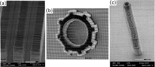
project patterns. Figure 9.42 shows an example of features that can be fabricated
using MSL.
716 D.R. Hines et al.
Fig. 9.42 Illustration of various structures fabricated using MSL: (a) microchannels, (b) gear, and
(c) microtube (Reprinted with permission from Elsevier, [141])
A limitation of single-photon processing is that polymerization occurs at the sur-
face of the vat. This can be overcome by using a two-photon process. The process
employs two intersecting i nfrared (IR) beams. At the point of intersection, the liq-
uid polymer can polymerize only by simultaneous absorption of two photons. This
produces a spot size below the diffraction limit of a single beam and allows the
polymerization to take place anywhere within the vat, not just at the surface. This
also allows for small structures that are truly 3-D. The two-photon absorption pro-
cess can take place either as a resonant excitation or a simultaneous absorption. In
the resonant-excitation mode the first photon is absorbed to create a real excited
state with a lifetime on the order of 10
−4
− 10
−9
s. Polymerization can occur only
if a second photon is absorbed by the monomer while in the excited state. In the
simultaneous absorption process, no intermediate excited state exists. Therefore
both photons must be absorbed within 10
−15
s of each other [142].
The two-photon absorption process is a nonlinear effect with polymerization
dependent on the square of the photon density. This phenomenon is responsible for
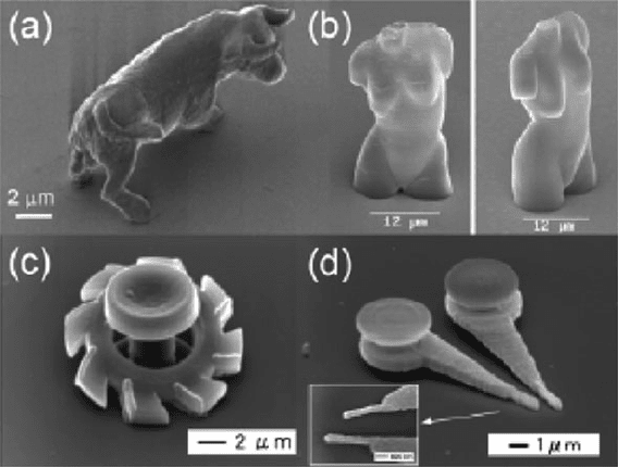
a resolution better than the diffraction limit of the single-beam profile. Figure 9.43
shows examples of features fabricated using two-photon MSL. Note that whereas
the features in Fig. 9.42 are in the hundreds of microns, these structures are on the
micron scale with submicron details!
9.6 Print/Imprint Lithography
Printing is an ancient art dating back to the eighth and ninth centuries A.D. An
example of such a printed work is the Diamond Sutra which was fabricated using
a technique referred to as block printing. Printing using movable type based on
clay [147] was invented in 1041 and based on metal [148] in 1232. Ushering in
a more modern style of printing, Gutenberg is credited with having invented the
9 MEMS Lithography and Micromachining Techniques 717
Fig. 9.43 3-D microstructures produced by multiphoton microfabrication: (a) microbull model
[143]; (b) Venus model [144]; (c) microturbine [145]; (d) nanotweezers [146] (Reproduced with
permission; copyright Wiley-VCH)
modern printing press in the 1450s. Lithography, which is a form of printing based
on a planographic process that relies on patterning inks onto a flat surface using
hydrophilic and hydrophobic interactions, was invented in 1798.
The semiconductor industry has developed a form of pattern transfer for the fab-
rication of solid-state electronics based on Si called photolithography. As described
in Section 9.2 above, photoresist is applied to and patterned on Si wafer substrates
in the manufacturing of computer chips and on glass substrates in the manufacturing
of flat-panel displays. Either way, the fabrication methods are limited to batch pro-
cessing of finite size substrates. Serious efforts are underway to develop larger-scale
manufacturing processes that can fabricate electronic devices in a continuous fash-
ion in a manner more similar to the fabrication of magazines or newspapers. In order
to accomplish this, the added requirement of flexible substrates will be needed.
As a testimony to the importance of such efforts, Xia and Whitesides [20] list no
fewer than 18 different nonphotolithographic patterning methods being developed
to fabricate devices at the micrometer and nanometer length scales. The table is
reproduced here as Table 9.5. The earliest reference dates back to 1974, with a
majority of the references coming from the 1990s. Even though printing is an old
technique with a rich history in fabricating and/or reproducing images and writing,
it is being revisited as a method for fabricating active electronic devices, circuits,
and MEMS components.

718 D.R. Hines et al.
Table 9.5 Nonphotolithographic methods for micro- and nanofabrication
a
Method Resolution
b
References
Injection molding 10 nm [149–154]
Embossing (imprint) 25 nm [155–163]
Cast molding 50 nm [164–166]
Laser ablation 70 nm [167–172]
Micromachining with a sharp stylus 100 nm [173]
Laser-induced deposition 1 µm[174–176]
Electrochemical micromachining 1 µm[177]
Silver halide photography 5 µm[178–180]
Pad printing 20 µm[181]
Screen printing 20 µm[182]
Inkjet printing 50 µm[24, 183–186]
Electrophotography (xerography) 50 µm[187, 188]
Stereolithography 100 µm[189–192]
Soft lithography [18, 21, 193, 194]
Microcontact printing (µCP) 35 nm [195, 196]
Replica molding (REM) 30 nm [197]
Microtransfer molding (µTM) 1 µm[198]
Micromolding in capillaries (MIMIC) 1 µm[199]
Solvent-assisted micromolding (SAMIM) 60 nm [200]
a
These numbers do not represent ultimate limits
b
The lateral dimension of the smallest feature that has been generated
Reproduced with permission from [20], copyright 1998,Wiley-VCH
Various types of printing techniques are reviewed here as they pertain to the pat-
terning and/or assembly of components needed to fabricate active electronic devices
and MEMS components.
The printing industry has been primarily interested in reproducing pictures and/or
text on a page. Both are passive features composed of two components: an ink
and a substrate (the page). The ink is designed for passive color and high visual
contrast against the substrate. The substrate can be made from various materials
such as paper, plastic, metals, glass, and so on. For the printing of active devices
the substrate materials may not change much but the inks will have to be very
different.
Visual contrast and passive color will no longer be important properties.
Admittedly, transparency over certain optical ranges may be important for some
applications; however, active inks will primarily be chosen for their conductivity,
semiconducting properties, insulating properties, and mechanical properties among
others. Such inks will need to be prepared and processed in ways that optimize
these properties. This will most likely require techniques very different from those
used to prepare and process passive inks, therefore traditional printing techniques
are not discussed. Rather, the discussion is dedicated to introducing and review-
ing printing methods being developed that will meet the needs for printing active
materials.
9 MEMS Lithography and Micromachining Techniques 719
9.6.1 Inkjet Printing
Inkjet printing [22] is a digital form of printing that can be performed either in
a continuous or a drop-on-demand mode. For the continuous mode, a stream of
droplets passes through a set of signal drive electrodes. An electrical pulse to the
electrodes causes a droplet to be deflected to the substrate. Undeflected droplets are
collected and recirculated back to the ink reservoir. For the drop-on-demand modes,
a piezoelectric pulse is used to create a droplet by pushing ink through a nozzle.
Nozzles are typically 20–30 µm in diameter and create ink droplets of about 10–20
pL. The droplet-on-demand mode results in better printing quality when compared
to continuous mode inkjet printing with feature resolution on the order of 20–50 µm
for standard inkjet printing.
Viscosity and surface tension are important parameters of the ink. Ink must fill the
nozzle in approximately 100 µs and not drip out between demands. This typically
requires a viscosity range of 2–100 cp and a minimum surface tension of about 35
mN/m. To prevent the ink from drying and clogging the nozzle, a liquid such as
ethylene glycol can be added at a level of 10–20%. If an ink contains particulates,
the particulates must remain uniformly suspended in the ink and not contribute to
clogging in the nozzle. This usually requires a particulate size less than 1 µm.
High-molecular-weight polymers tend to be too viscous to print easily using
inkjet printing. However, inkjet printing of waxy and low-molecular-weight poly-
mers is possible. Printed droplets can exhibit pinholes and can have a tendency to
bead up when printed onto nonabsorbent substrates (such as plastics). Also, edge
roughness and printing resolution can be affected by droplet-spreading character-
istics and can be difficult to control. Some materials’ printing problems can be
overcome by incorporating additives into the ink that can be postprocessed, such as
the addition of UV curable polymers. Also precursor materials can be used directly
as inks that are postprocessed, such as precursor metal solutions.
A wide range of materials has been successfully inkjet printed. Calvert [22]
lists nanoparticle suspensions, sol-gels, conducting polymers, ceramic powders, sol-
der, DNA, and proteins as materials that have been inkjet printed, all of which
must either be suspended or dissolved. Some organic semiconductor materials
tend to be insoluble (pentacene, e.g.) and, therefore, soluble forms of these mate-
rials have been investigated for use in specific inkjet applications [201]. Other
organic semiconductor materials tend to be very sensitive to drying conditions such
as poly(3-hexylthiophene) (P3HT) [202]. In either case, inkjet printing of these
materials has, to date, typically resulted in low-quality films.
There have been attempts to improve the resolution associated with inkjet print-
ing. One method used an undisclosed print head technology as part of a superfine
inkjet printing system [203]. This system was reported to have achieved a line width
of 3 µm. Also, Sirringhaus et al. have developed a droplet-on-droplet technique in
which the second droplet does not wet the first droplet [204]. When printed, the
second droplet slides off the first droplet, producing a sub-100 nm gap between
the printed features, which are then used as source/drain electrodes for an OTFT
device.
720 D.R. Hines et al.
9.6.2 Soft Lithography
Photolithography has been used for decades in the fabrication of inorganic elec-
tronics; however, it has several disadvantages that limit its usage for nontraditional
materials: it allows for very little variation in the chemistry of either the resist layer
or the substrate and it can only be performed on flat surfaces in a batch-processing
mode.
In an attempt to go beyond the limitations of photolithography, soft lithographic
methods have been developed, as listed i n Table 9.5. Soft lithography encompasses
techniques such as microcontact printing [195, 196](µCP), replica molding [197]
(REM), microtransfer molding [198](µTM), micromolding in capillaries [199]
(MIMIC), and solvent-assisted micromolding [200] (SAMIM). These t echniques all
have in common a patterned elastomeric mold or stamp (typically made from poly-
dimethylsiloxane (PDMS)). Because the stamp (mold) is flexible, these techniques
are compatible with nonflat surfaces.
Soft lithography techniques have also been used to print patterned layers from
PDMS stamps onto substrates. For example, Au evaporated onto the patterned sur-
face of a PDMS stamp and then treated with a thiol- terminated self-assembled
monolayer (SAM) has been printed onto a GaAs substrate [205]. Also PDMS fea-
tures have been printed onto Si substrates by treating the patterned surface of a
PDMS stamp with a fluorinated SAM and then adding an extra layer of PDMS
[206]. When contacted to the Si substrate, the top layer of PDMS can be transferred
to the Si surface. Childs and Nuzzo [206] provide detailed procedures for preparing
PDMS films and bonding such films to Si substrates to produce both closed and
open patterns on the substrate. Below, a case study is provided for the preparation
of PDMS films.
Unlike photolithography, which transfers a pattern using optical techniques, soft
lithography is a direct printing method. Also, the stamp (mold) can be replicated
from a reusable master template. Therefore, soft lithography has the potential to be
a less complex and less expensive method of patterning compared to photolithogra-
phy. In addition, soft lithographic techniques can be used to directly pattern a wider
range of surfaces comprised of polymers, sol-gels, biological materials, organic
thin-films, and colloidal materials, in addition to inorganic surfaces.
9.6.3 Nanoimprint Lithography (NIL)
In addition to the limitations discussed above, pattern sizes produced by pho-
tolithography are limited by the resolution of the optical system used to transmit
light through the mask. Over decades of research, this resolution limit has been
steadily reduced at the expense of increased complexity and cost of the fabri-
cation equipment. Nanoimprint lithography (NIL) [156] has been developed as a
patterning technique that can simultaneously improve pattern resolution and reduce
both equipment complexity and cost. It is based on a rigid template containing a
9 MEMS Lithography and Micromachining Techniques 721
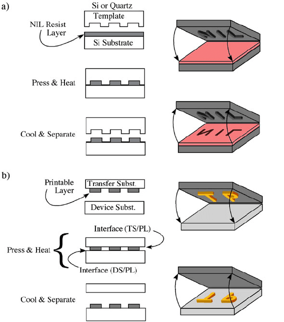
Fig. 9.44 (a) Nanoimprint lithography (NIL) and (b) the transfer printing method (Reprinted with
permission from [219], copyright 2007)
patterned surface. The template is pressed into a resist layer that has been coated
onto a substrate. Two types of NIL have been developed and are referred to as
hot and cold embossing. Hot embossing uses a thermoplastic resist layer and cold
embossing uses a UV-curable liquid layer. The general process is illustrated in
Fig. 9.44a.
In hot embossing, the patterned template surface is placed in contact with the
thermoplastic resist layer. The resist layer is heated up above its glass transition
temperature and the template is pressed into the resist layer. After a specified time
the resist layer is cooled down below its glass transition temperature and the pressure
is released. The template is then removed to reveal a replica of the template surface
contained in the surface of the resist layer.
In cold embossing, sometimes referred to as step-and-flash imprint lithography
[207] (SFIL), the patterned template surface is placed in contact with a UV-curable
liquid layer. The resist layer is then cured by exposure to UV light. The template
722 D.R. Hines et al.
is then removed to reveal a replica of the template surface contained in the surface
of the resist layer. In this case, the template (or possibly the substrate) must be
transparent to UV light. This is similar to replica molding [197] which typically
uses a flexible template, however, SFIL has been developed using a rigid t ransparent
template.
Several variations of hot embossing have been reported [208, 209] as a means
of reducing the operating pressure and/or temperature. One technique eliminates
the resist layer entirely [210]. NIL is also being expanded to include imprinting
into a variety of active materials as opposed to sacrificial resists [211]. The reso-
lution of NIL has been demonstrated to be at the 10 nm level [212]. Most of the
developmental work associated with NIL is directed toward inorganic substrates
and is targeted as a disruptive technology competing against photolithography and
e-beam lithography. Schift [213] provides a review article that discusses a wide vari-
ety of processing issues and materials parameters associated with conventional NIL.
NIL techniques have begun to enter the realm of MEMS fabrication largely asso-
ciated with microfluidics applications incorporating small-diameter flow channels.
Nanochannel fabrication for applications involving DNA stretching and sequencing,
protein separation, and drug delivery are discussed by Kim et al. within Chapter 13
in the book Unconventional Nanopatterning Techniques and Applications [15].
Many variations of NIL are being developed in order to address specific
applications that are not so easily accomplished by conventional techniques. For
example, rather than competing with photolithography, NIL can be combined with
photolithography to simultaneously pattern large and small features. Work on com-
bining nanoimprint and photolithography (CNP) [214, 215] uses a hybrid mold that
is at once both a photomask and an NIL template. In addition, large volume roll-
to-roll NIL (R2RNIL) has also been envisioned for high-speed manufacturing. A
body of work designed to integrate NIL fabrication methodologies into MEMS-
based systems is beginning to emerge in the literature. S. Park and H. Schift have
contributed an entire chapter discussing NIL technology for biological application
in a book devoted to bio-MEMS [216]. A variety of topics is presented such as
nanofluidic devices, engineered nanopores, and nanopatterns defined by variations
in surface chemistry or protein coverage. Applications such as battery and fuel
cell technologies can greatly benefit from increased surface area coatings. Zhang
et al. have incorporated NIL processing methods into the design and fabrication of
MEMS-based fuel cells as a means for increasing reaction surface areas among fuel,
catalyst, and electrolytes [217]. X. Fan et al. has utilized NIL as a low-cost method
for the fabrication of PMMA microlens arrays on a Si substrate [218].
9.6.4 Transfer Printing
As is illustrated in Fig. 9.44b, the same processing method used for NIL can be
used to transfer a patterned layer (printable layer) from one substrate (the transfer
substrate) to a second substrate (the device substrate). The only requirement is that
9 MEMS Lithography and Micromachining Techniques 723
the printable layer adheres more strongly to the device substrate than to the transfer
substrate. This process is referred to as transfer printing. In general, the transfer
printing process does not rely on temperature, but only on contact of the printable
layer to the surface of the device substrate where an appropriate differential adhesion
exists between the two interfaces containing the surfaces of the printable layer. This
is the same governing principle seen in decals for detailing model cars and airplanes
or for a child’s temporary tattoos.
It is with such a process that we wish to develop the ability to fabricate flexi-
ble electronics and MEMS devices. Plastic substrates present an obvious choice of
materials for this application, not only because they are flexible, but also because
of their low density, optical clarity, low cost, compatibility with roll-to-roll process-
ing, and so on. The process is simple in concept but has the potential to allow a
wide variety of dissimilar materials to be combined onto a single substrate in ways
difficult if not impossible to achieve with conventional methods. Figure 9.45 shows
examples of metallic, organic, and carbon-based materials that have been printed
onto a plastic substrate.
Figure 9.45a illustrates a 50 µm wide serpentine Au electrode printed onto a
Kapton substrate. The Au feature was fabricated on a Si wafer transfer substrate
using standard photolithography. Prior to printing, the transfer substrate was spin
coated with a l ayer of polyimide. The Au/polyimide bilayer was then printed onto
the Kapton substrate. The profilometer scan shows that the printed Au feature pro-
trudes above the Kapton surface. In general, Au features from 200 nm wide lines up
to full 3 in. diameter films have also been successfully printed onto PET substrates.
Figure 9.45b illustrates a 50 nm thick pentacene film printed onto a PET sub-
strate. In t his example, a Pn film was thermally evaporated onto a SiO
2
/Si wafer
transfer substrate. Prior to printing, an Au electrode was evaporated onto the transfer
substrate such that it also partially covered the Pn film. The three resulting r egions
(Au, Au/Pn, and Pn) were all successfully transfer printed onto the PET substrate.
Pn has also been printed onto Au, PC, latex, nitrile, PVC, and PMMA surfaces, to
name a few examples. In addition, Pn films can be patterned by printing against a
patterned photoresist film.
Figure 9.45c shows an example of a CNT network printed onto a PET substrate
that contains previously printed Au electrodes. The CNT network was grown by
CVD onto a SiO
2
/Si wafer transfer substrate. Similarly, graphene has also been
printed onto Au and polymer surfaces.
The last example shown in Fig. 9.46 illustrates the ability to print inorganic fea-
tures directly onto a prepatterned plastic or elastomer substrate. Here a Si grid is
shown printed onto a patterned PC substrate. Others have used PDMS as an inter-
mediate substrate for the printing of Si features using a kinetic printing process
where the adhesion is controlled by the speed at which the intermediate substrate
is removed. For all these illustrations, adhesion to the first substrate must be less
than adhesion to the final substrate. Efforts to establish printing parameters for a
wide variety of materials have relied on the engineering of surface energies. Self-
assembled monolayers (SAMS) can provide an easy effective tool for establishing
the desired surface energy of a given substrate [222]. For example, the adhesion of
