Ghodssi R., Lin P., MEMS Materials and Processes Handbook
Подождите немного. Документ загружается.

684 D.R. Hines et al.
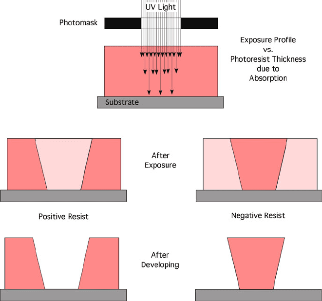
material will be dissolved away at the top than at the bottom of the exposed area.
For a positive photoresist, such an exposure profile versus depth results in an “over-
cut” sidewall profile (a sidewall angle less than 90
◦
). This is acceptable for etching
applications but not for “liftoff” applications. For a negative photoresist, such an
exposure profile versus depth results in an “undercut” sidewall profile (a sidewall
angle greater than 90
◦
). This is desirable for liftoff applications but can result in
loss of pattern fidelity for etching applications. Ideal, overcut, and undercut sidewall
profiles are illustrated in Fig. 9.17.
Fig. 9.17 Edge profile of photoresist layer resulting from absorption of light during exposure
9.2.3.1 Positive Photoresist
Upon exposure to light, the solubility of a positive photoresist increases due to poly-
mer chain scission. Common formulations of positive photoresists have included
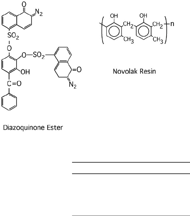
diazoquinone ester (DQ) as a sensitizer in a novalac resin (phenol formaldehyde
resin) (N). These molecules are shown in Fig. 9.18. Such formulations are referred
to as DQN resists. A typical DQN resist formulation is listed in Table 9.2.
9 MEMS Lithography and Micromachining Techniques 685
Fig. 9.18 Chemical formulas of (a) diazoquinone ester and (b) novolak resin components of
standard positive photoresists (Reprinted with permission from [7])
Table 9.2 Photoresist
components for positive DQN
resist
Resist component Weight, g
DQ 2
Novolak 8
Cellosolve acetate 20
Butyl acetate 2
Xylene 2
Water (trace) 0.05
Reprinted with permission from [7]
DQN-based resists are insensitive to oxygen and work very well at near ultravio-
let (UV) wavelengths provided by the 365 (i-line), 405 (h-line), and 435 (g-line) nm
lines of an Hg lamp typically found in research and development cleanroom facili-
ties. For deep UV (DUV) (248 nm) and extreme UV (EUV) (193 nm) applications,
positive photoresist formulations that do not contain aromatic molecules, such as
PMMA-based materials, need to be utilized. A 15% loading of the photoresponsive
DQ is enough to photochemically transform the two-component resist into a polar
(base) soluble product upon exposure to UV light [7].
Positive resists are generally more expensive than negative resists; however,
they exhibit higher pattern resolution causing them to be more widely used for
photolithographic processing applications. Positive resists do not tend to swell
when submerged in developer and can be developed in aqueous-based solvents
that decrease the amount of generated hazardous waste material. Photochemical

686 D.R. Hines et al.
reactions in a positive resist are not sensitive to oxygen and the phenolic resin com-
ponent provides plasma etch resistance to the resist. DQN-based positive resists
can be thermally stabilized to 200
◦
C and are suitable for use for image reversal.
However, they tend to have a narrower processing window and exhibit lower wet
chemical etch resistance and lower adhesion to substrate surfaces. For this reason an
adhesion promoter such as hexamethyldisilazane (HMDS) is applied to the substrate
surface prior to coating the substrate with a photoresist layer [7, 36].
Commonly used positive resists include Shipley 1813 and Fujifilm OiR-906-10.
Processing case studies are included below for both of these resists. Other common
formulations of positive photoresist are shown in Table 9.3.
Table 9.3 Commonly used positive photoresists
Polymer References from Moreau
Polyhydroxystyrenes [23, 185]
Polyvinylphenol [24]
Styrene-methacrylic acid [25, 186]
PMMA-methacrylic acid [26]
Styrene-acrylic acid [27]
Esterified polyvinyl alcohol [28]
Polyimide [29]
Silylated novolak [30, 211]
Reprinted with permission from [7]
9.2.3.2 Negative Photoresist
Upon exposure to light, the solubility of negative photoresists decreases due either
to cross-linking of the polymer chains or a photochemical reaction. Many polymers
will cross-link when exposed to light. Various types and classifications of negative
photoresists are listed in Table 9.4.
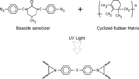
An early negative photoresist formulation referred to as KTFR combined a bis-
aryldiazide photosensitive cross-linking agent with a polyisoprene cyclized polymer
as shown in Fig. 9.19 [7, 37, 38].
Such resists suffer from sensitivity to oxygen and solvent swelling. To over-
come such deficiencies, onium salts [39, 40] were identified as photosensitive
Table 9.4 Classifications and types of negative photoresists
Thermoset Elastomers Thermoplastics
Diallylphthalates Acrylates Acetates
Epoxies Polysulfides Acrylates
Phenolics Neoprenes Cellulosics
Urethanes Polycarbonates
Silicones Polystryenes
Polyimides
Reprinted with permission from [7]
9 MEMS Lithography and Micromachining Techniques 687
Fig. 9.19 Negative photoresist components before and after exposure to UV light (Reprinted with
permission from [38])
additives that, when exposed to light, catalyze (chemically amplify) cross-linking
or decreased solubility.
Negative resists are not widely used for photolithographic processing applica-
tions because they exhibit a lower pattern resolution in comparison to positive
resists. They also tend to swell when submerged in developer. Negative resists are
cheaper and have higher chemical resistance than positive resists. They are also
more adhesive to substrate surfaces and harder to remove after processing. In addi-
tion, negative resists exhibit larger processing windows and can be formulated from
a wide variety of polymers.
Common types of negative resist include chemically amplified epoxy or vinyl
derivatives. A case study of the common Futurrex NR7-1500PY is presented below
[30, 38].
For MEMS processing, SU-8 has recently become a commonly used negative
resist material. SU-8 was first developed by IBM in 1989 and is now sold by
MicroChem Corporation. SU-8 is highly transparent above 360 nm. This means
that UV light can penetrate through a thick layer (up to about 2 mm). The lack of
absorption results in nearly vertical sidewalls, thus allowing the fabrication of SU-8
structures with very high aspect ratios (>20). Because of this unique feature SU-8 is
not usually used as a sacrificial pattern transfer layer but rather as a patterned poly-
mer layer that is permanently incorporated into device fabrication. SU-8 is presented
in more detail in Chapter 5.
9.2.3.3 Image Reversal for Positive Resist (Converting Positive Resist
into a Negative Resist)
Because of the typical overcut sidewall edge profile in a positive photoresist, it is not
suitable for liftoff processes. Also, a negative resist is not as attractive as a positive
688 D.R. Hines et al.
resist in many applications because of lower resolution and the generation of larger
amounts of hazardous waste. Therefore, image reversal processes have been devel-
oped that enable a positive resist to be used to produce a negative tone image. The
image reversal process for a positive resist is accomplished by postbaking the resist
layer in an ammonia vapor oven [31, 41–43]. The interaction of the ammonia with
the UV exposed regions of the photoresist (i.e., soluble regions) renders the pho-
toresist insoluble and also insensitive to further UV exposure. A subsequent flood
exposure converts the previously unexposed regions of the photoresist to a soluble
form. Thus, upon developing, the initially unexposed regions of the photoresist are
dissolved away leaving a negative image of the initial photomask pattern.
9.2.4 Substrate
Historically, MEMS and IC fabrication have been performed using Si, Ge, or GaAs
substrates. Flat panel displays are typically fabricated on glass substrates. More
recently, microfluidic devices, lab-on-a-chip, and flexible electronics have incor-
porated polymeric substrates. Often transparent substrates can be more challenging
to perform lithography on, as the reflection or lack thereof can broaden exposure
regions, or reduce the dose directed to the photoresist. In all cases, photolithogra-
phy demands that the substrate be flat and well cleaned. Inorganic s ubstrates can
be cleaned in several ways: for example: RCA clean, plasma (or UVO) clean, or
solvent clean.
9.2.5 Processing Steps for UV Lithography
9.2.5.1 Deposit Photoresist
Spin Coating
Photoresist is typically applied t o substrates via spray or spin coating. Although
spin coating is a rather simple process, the tolerances for film thickness, unifor-
mity, and repeatability raise a number of important issues that must be understood
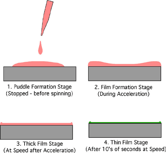
and controlled. As illustrated in Fig. 9.20, there are typically four stages of film
evolution during the spin-coating process. The puddle formation stage results from
the dispensing of the photoresist onto the substrate surface prior to spinning. The
photoresist at this point is a thick puddle that covers some or all of the substrate.
The film formation stage develops during acceleration of the spin coater as spinning
commences.
The photoresist at this point covers the entire substrate, is starting to thin out at
the center of rotation and is getting thicker toward the edges of the substrate. The
thick-film stage develops after acceleration when the spin coater has reached the
desired spin speed. The photoresist at this point is a relatively uniform but thick
film (tens to hundreds of microns thick) that may contain thickness variations near
9 MEMS Lithography and Micromachining Techniques 689
Fig. 9.20 Stages of film evolution during the spin coating process (Modified from [44] and used
with permission)
the edge of the substrate. The thin-film stage develops after tens of seconds at the
desired spin speed. The photoresist at this point is approaching its target thickness
over the entire area of the substrate and may still have thickness variations only at
the very edge of the substrate. As the film progresses from the thick-film stage to
the thin-film stage, optical interference fringes resulting from reflection off both the
top surface of the resist layer and the interface between the resist and substrate can
be seen to change color as it gets thinner. Viewed at an appropriate angle, these
thickness fringes can be seen to appear at the center of the wafer and rapidly travel
radially out to the edge of the wafer while the wafer is spinning.
Several artifacts can appear in the photoresist as a result of spincoating: (1) stri-
ations that are nonuniformities in thickness typically on the order of 30 nm caused
by nonuniform drying of the resist after spin coating; (2) edge effects that result
from excess resist buildup at the wafer edge that can be 20–30 times thicker than
the resist layer; and (3) streaks caused by particulate contamination on the surface
of the substrate or in the resist itself.
As IC feature sizes decrease, resist thickness must also decrease. For MEMS pro-
cessing however, such state-of-the-art feature sizes are typically not encountered.
Rather, MEMS processing may require thicker resist layers that cover surfaces con-
taining intricate topology, thus defining a different set of r esist constraints t hat affect
690 D.R. Hines et al.
viscosity, solvent evaporation rates, and so on. Such constraints must be factored
into the production of flat, uniform, stress-free films.
After spin coating, the remaining solvents must be removed from the resist film.
This is typically performed with a prebake (or soft-bake) on a hotplate or in an oven.
On a hotplate the temperature increase of the photoresist starts at the bottom of the
film and progresses upward. This prevents solvent vapors from getting trapped in the
film during the prebake. In contrast, in an oven the temperature rise is more uniform
throughout the film which can decrease the rate at which solvents are driven out
of the film. In an oven, the top surface of the photoresist can form a skin that may
trap solvent vapors and subsequently form bubbles or other imperfections in the
resist layer. For this reason, prebaking in an oven is typically a slower process than
prebaking on a hotplate.
Spray Coating
For substrates that have very nonuniform surfaces or deep trenches and tall features,
as is common with MEMS processes, spin coating will not be able to produce a uni-
form photoresist coating. In cases such as these, the more commonly used method is
spray coating [45, 46]. In a spray coating system, photoresists are mixed in different
ratios with solvents to facilitate the spraying onto the surfaces of the wafer [47]. In
the spray-coating process, there is direct perpendicular impingement of the coating
solution that promotes coverage into deep trenches and along tall features. This is
usually achieved by a reciprocating spray nozzle that coats the wafer surface to the
desired photoresist thickness. For thicker films, the solutions used in spray coating
are often diluted as compared to that used to achieve a similar spin-coated film thick-
ness. These systems are critical to the fabrication of many high-aspect-ratio MEMS
structures. Unfortunately, very few commercialized spray coating photoresists exist
and most need to be mixed and characterized on a case-by-case basis [47].
9.2.5.2 Expose Photoresist
For a positive photoresist layer, the solubility of certain well-defined areas can be
increased by the exposure to UV light. In contrast, for a negative photoresist layer,
the solubility of certain well-defined areas can be decreased by the exposure to UV
light.
This is performed by mounting a photoresist coated wafer and a photomask con-
taining the desired mask pattern into an optical projection system (i.e., a contact
aligner or stepper). The mask pattern and wafer are aligned in X, Y, Z, and Rotation
as needed. Once properly aligned, UV light is transmitted through the mask to
expose the desired area of the photoresist layer as described above. Depending on
the resist properties, a postexposure bake may be necessary to achieve the desired
solubility change in the exposed region of the resist layer.
9 MEMS Lithography and Micromachining Techniques 691
9.2.5.3 Develop Photoresist
After exposing selected areas of the photoresist layer to UV light, the soluble regions
can be removed by submerging the photoresist coated wafer in a solution of the
appropriate solvent. A 30–90 s soak is typically sufficient to wash away the soluble
regions of the exposed photoresist layer. To halt the developing process, the wafer is
removed from the developer solution and then typically submerged into a deionized
(DI) water bath for approximately 30 s and dried in a stream of clean/dry N
2
gas.
At this point the photoresist layer should contain a pattern of open areas identical
to the mask pattern. A careful inspection of the open areas and sidewalls with a
high-powered optical microscope is recommended.
If there is any photoresist visible in the open areas then either the photoresist
was not exposed to enough UV light or it was developed for too short a time. If the
photoresist was underexposed then the lithography process will need to be repeated
with a fresh layer of photoresist and a longer exposure time. If the photoresist was
underdeveloped, the photoresist layer can be returned to the developing bath for a
short time. It is noted that there exist a large number of developer solutions that
can be used to an equal effect. In most cases, however, manufacturers of photore-
sist create various developers that are specifically optimized to be used with each
photoresist and should be consulted when developing a more detailed or sensitive
process flow.
9.2.5.4 Transfer Pattern
The patterned photoresist layer covering the surface of a substrate contains areas that
are “open” (i.e., where the photoresist has been removed). At this point material can
either be added to or removed from the substrate surface within these open areas.
Removing material is called etching. Wet etching techniques are presented in
Chapter 8. Dry (plasma) etching techniques are presented in Chapter 7. Etching
processes rely on the photoresist having a much slower etch rate than the substrate
surface. The fidelity of the pattern transfer as a result of the etching process depends
both on how directional the etch process is and on the profile of the photoresist side-
wall at the edge of the open areas. If the photoresist sidewall is perfectly vertical
and the etch rate in the horizontal direction is zero (i.e., perfectly anisotropic) then
the pattern developed into the photoresist layer will be perfectly transferred into the
substrate surface due to the etching process. Any deviations in the perfection of the
photoresist sidewall will correspondingly result in removing more substrate mate-
rial than desired. Etch rates that are not perfectly anisotropic will either produce less
than vertical sidewall profiles in the substrate (sidewall angle less than 90
◦
), under-
cut beyond the edge of the photoresist opening (sidewall angle greater than 90
◦
)
or over etching (features in the substrate surface that are larger than the openings
defining the photoresist pattern).
Adding material is referred to as deposition. Deposition of semiconductor
and dielectric materials is presented in Chapter 3 and deposition of metals in
692 D.R. Hines et al.
Chapter 4. Typically material is added over the entire substrate thus covering the
photoresist surface and the substrate surface that is accessible in the open areas of
the patterned photoresist layer. The process of photoresist depositing and develop-
ing can leave a thin invisible residue on the substrate surface in the open areas of
the photoresist pattern. This residue can cause a decrease in t he adhesion of the
deposited layer to the substrate surface and should be removed prior to deposition.
This residue layer is typically removed by performing a low-power oxygen plasma
etch (sometimes referred to as a descum) just prior to materials deposition.
9.2.5.5 Remove Photoresist
Once deposition is completed, the unwanted material has to be removed from the
surface of the photoresist and also the photoresist removed. For a method that
includes an additive process, this is accomplished all in one step called “liftoff”.
Liftoff is performed by submerging the substrate (covered with the photoresist and
deposited layers) into a solvent bath. The solvent dissolves the photoresist l ayer
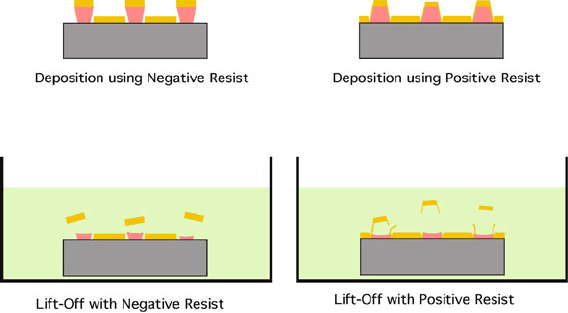
thus causing the deposited layer on the photoresist surface to float away. Lift-off
processes can be slow because the photoresist has very little surface area exposed
to the solvent. The processing time can be decreased by increasing the temperature
of the solvent bath. Also applying the solvent in the form of an aerosol spray can
help the liftoff process. For this to work properly the deposited layer must be dis-
continuous at the edges of the opening in the patterned photoresist. Therefore the
photoresist sidewall profile should be undercut. For this reason, negative photore-
sists or positive photoresists with image reversal work best for liftoff applications
inasmuch as they inherently have undercut profiles. This is illustrated in Fig. 9.21.
For processes that involve etching rather than deposition, only the photoresist
layer needs to be removed after substrate etching. Photoresist is typically removed
in one of two ways: either using the appropriate solvent or using plasma etching
Fig. 9.21 Illustration of liftoff with positive and negative resists
9 MEMS Lithography and Micromachining Techniques 693
(sometimes referred to as ashing). Acetone is the most common solvent for photore-
sist in the cleanroom and is usually sufficient to clean the surface. In some cases,
the photoresist can be more difficult to remove, such as after successive baking steps
or etching steps, and for these cases the photoresist manufacturers provide specific
photoresist solvents, usually called “strippers,” or “resist removers.” These solvents
tend to be much more aggressive than acetone, and may damage other materials on
the surface of the wafer. Care must be taken when using these solutions to remove
photoresist.
Plasma etching to remove photoresist is more s traightforward. “Ashing” con-
sists of an O
2
plasma that chemically reacts with and consumes organic matter on
the wafer, and thus the photoresist. In some cases an argon plasma can be used to
remove photoresist, but in this case the argon plasma merely physically sputters the
photoresist material away and can damage other materials on the wafer. In many
situations ashing is preferred over some of the more aggressive solvent options, but
it is noted that the plasma techniques do not always remove photoresist, such as is
the case with some negative resist formulations that are less reactive.
9.3 Grayscale Lithography
UV lithography processing methods presented in the previous section strictly per-
tain to high-resolution, 2-D patterning on flat substrates. Great effort has gone
into producing near-vertical sidewalls for etching applications and slightly under-
cut sidewalls for liftoff applications. This is fine for the semiconductor industry,
however, there are MEMS-based applications where precise control over the side-
wall profile of the photoresist and subsequent etch processing is highly desirable.
For example, applications in the area of optics [48–50], microfluidics [51], and pho-
tonic crystals [52] require the ability to apply 3-D fabrication methods to MEMS
substrates.
Two-dimensional lithography photomasks are designed to either block or trans-
mit light. The resolutions of these masks are diffraction limited. The primary goal
is to completely expose and subsequently remove all the photoresist from spe-
cific area(s) on the coated substrate. In 3-D lithography applications, the goal is
to pattern the photoresist such that the patterned photoresist layer is comprised of
areas containing variable thickness profiles. To accomplish this, both the photomask
and the photoresist properties can be manipulated. For the photomask [53–62], the
opaque areas that define the pattern can be modified to be partially transparent. An
illustration of this is shown in Fig. 9.22.
There are a number of methods that can be used to achieve this. One method
uses commercially available high energy beam sensitive (HEBS) glass that uses the
beam-induced reduction of silver ions in a silver–alkali–halide material to produce
the darkening of the glass via coloring specks of silver atoms. This directly modu-
lates the opacity of the photomask with no graininess. HEBS glass mask resolution
is limited only by the beam writers, and examples of sub-0.25 µm features have
