Ghodssi R., Lin P., MEMS Materials and Processes Handbook
Подождите немного. Документ загружается.

704 D.R. Hines et al.
X-ray radiation
Proximity gap
1)
2)
3)
4)
5)
6)
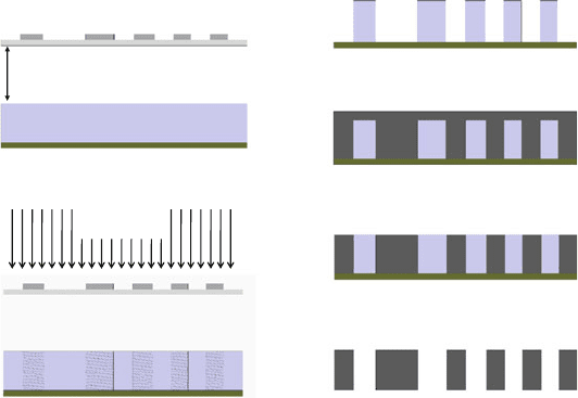
Fig. 9.31 X-ray lithography process. Steps 4–6 are unique to the LIGA micromachining method.
(1) Mask is fabricated with transparent membrane and metal absorbing pattern and brought within a
proximity to a conductive substrate coated with PMMA or other thick X-ray photoresist. (2) X-ray
radiation exposes PMMA resist. (3) Development of PMMA. (4) Metal is plated into the PMMA
mold (nickel, gold, copper). (5) Wafer is lapped to remove the metal cap; for mold fabrication, this
step may be omitted. (6) Substrate and PMMA are removed and the metal mold/part is ready for
additional processing or assembly
and injection techniques that can be used for the final LIGA fabricated structures
are explored in more detail in Chapters 4 and 5.
9.5 Direct-Write Lithography
The lithographic processes discussed above include the use of a mask for patterning
a layer of resist. It is also possible to pattern the resist layer directly by forming
the source into a narrow beam and scanning it across the surface of the resist. By
blocking the beam or scanning it in a desired fashion, the resist layer can be exposed
pixel-by-pixel. After exposure, the r esist layer can then be further processed just as
it would have been had it been exposed through a mask in the photolithographic
method. Electron beams, ion beams, and laser beams can all be used in such direct-
write techniques.
9.5.1 E-Beam Lithography
Electron-beam (e-beam) lithography uses electrons to expose a resist layer. Like
photons in photolithography, the solubility of a resist layer can be changed due to
interactions with electrons. By scanning the electron beam across the surface of the
9 MEMS Lithography and Micromachining Techniques 705
resist layer in a fashion almost identical to scanning electron microscopy (SEM),
the resist layer can be patterned. In an SEM, magnetic or electrostatic deflectors are
used to scan or raster the beam across the surface of the resist layer. Added to this
is the means to blank the beam by inserting electrostatic plates into the column that
can deflect the beam so that desired areas (or pixels) are left unexposed. Dedicated
systems that have been designed solely for e-beam lithography can provide state-
of-the-art capabilities. However, in many research and development labs, e-beam
lithography is performed using an SEM fitted with a beam blanker controlled by
a separate computer running commercially available SEM lithography software. A
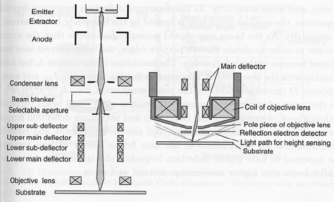
diagram of the scanning and beam blanking of an SEM-based e-beam lithography
system is shown in Fig. 9.32.
Fig. 9.32 Illustration of an e-beam lithography system (Reprinted by permission from [90])
For a Gaussian beam focused using magnetic lenses, a resolution of 10 nm
or less is possible with e-beam lithography. The exposure speed is too slow,
however, for large-scale production and is therefore typically used for mask fab-
rication, prototyping, or research and development applications. For example,
photomasks and nanoimprint lithography templates are routinely fabricated using
e-beam lithography due to the high resolution available.
Depending on the magnification setting of the microscope during writing, the
electron beam can only be scanned over a finite area (e.g., a 100 × 100 µm area).
To pattern larger areas, exposed areas can be “stitched” together by moving the
substrate to a new area and continuing the exposure. This is similar to the action of
a stepper but with e-beam, the subsequent exposures do not have to be identical and
can be connected.
706 D.R. Hines et al.
E-beam lithography is capable of producing high-resolution patterns, thus it is
also well suited for NEMS applications. Many NEMS devices incorporate mechani-
cal resonators, cantilevers, and doubly clamped beams. Applications involving mass
sensing with cantilevers have a mass in the ictogram and mass detection capabil-
ity in the attogram [91] and zeptogram [92] range. Ekinci and Brugger [93]give
an account of fabrication of NEMS cantilevers from Si, GaAs, AlGaAs, AlN, SiN,
SiC, and nanocrystalline diamond all fabricated using e-beam lithography. The res-
olution achievable with e-beam lithography is limited by machine stability, beam
diameter, and proximity effects. Yamazaki [90] gives an account of several factors
associated with machine stability that can affect pattern resolution.
As the electron beam interacts with the resist layer and the underlying substrate,
electrons can be scattered or absorbed. The scattered electrons can contribute to
unwanted exposure in nearby areas of the photoresist layer. This type of exposure
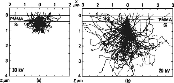
error is referred to as the “proximity effect.” A Monte Carlo simulation of electron
scattering for PMMA resist on a silicon substrate is shown in Fig. 9.33 [94]. Three
main types of electron scattering are important in e-beam lithography: forward
scattering, backscattering, and secondary electron emission. Forward scattered elec-
trons can be minimized by using thin resist layers and high acceleration voltages.
Backscattered electrons are largely responsible for proximity effects. Secondary
electrons are a cascade of low voltage electrons that are created from the interaction
of primary beam electrons with the resist or substrate materials. Secondary electrons
produced within the resist layer account for the bulk of the resist exposure dose and
can cause beam broadening on the order of 10 nm. Because secondary electrons
have low energy, they travel only a short distance within the resist and thus do not
contribute much to proximity effects.
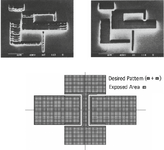
The proximity effect is highlighted in Fig. 9.34a for an uncorrected exposure.
Note that larger and more closely spaced features are more fully developed (less
Fig. 9.33 Simulation trajectories for electrons in PMMA film on Si substrate (Reprinted with
permission from [94], copyright 1975, American Vacuum Society)
9 MEMS Lithography and Micromachining Techniques 707
(c)
(a)
(b)
Fig. 9.34 Examples of proximity effect corrections (a) uncorrected exposure (noted by residual
resist in patterned areas), (b) corrected exposure using dose modulation and (c) schematic illustrat-
ing the pattern biasing technique ((a)and(b) reprinted with permission from [97], copyright 1981,
American Vacuum Society)
residual resist). To some extent, proximity effects can be minimized by assigning
different dose rates to different sized features. Also film thickness and beam energy
can be adjusted to minimize beam scattering under certain controlled settings. The
most common way to correct proximity effects is to modulate the dose rate. There
are several dose modulation techniques [95, 96] based on calculations that solve
the shape-to-shape interactions. If the dose for a large-area feature is normalized to
unity, then smaller and isolated features are assigned a somewhat larger dose. The
result of the dose modulation proximity effect corrections is shown in Fig. 9.34b.
An alternative approach to proximity effect corrections is to bias the patterning [95,
96]. As illustrated in Fig. 9.34c, pattern biasing compensates for the overdosing of
closely spaced features by slightly reducing the size of the patterns. This is more
easily implemented within an e-beam writing system but does not have the dynamic
range of dose modulation.
Polymethylmethacrylate (PMMA) is a standard positive e-beam resist. Other
resist materials include poly(2,2,2-trifluoroethyl--chloroacrylate) (EBR-9) which
is an acrylate-based resist that is commonly used in mask writing applications
and is ten times faster but also has ten times lower resolution t han PMMA,
and poly(butene-1-sulfone) (PBS) which is a high-speed positive e-beam resist
708 D.R. Hines et al.
commonly used for photo mask patterning. See [98] for a more detailed discus-
sion about different e-beam resists. A case study of PMMA e-beam resist is given
below. For liftoff applications, a bilayer resist is typically applied to the substrate.
For example, the 200-nm layer of methylmethacrylate (MMA) is spin coated onto
the substrate and baked. A subsequent 200-nm layer of PMMA is then spin coated
onto the substrate and baked. The MMA is more sensitive to the e-beam exposure
than PMMA so it dissolves away at a faster rate during development producing an
undercut below the edges of the PMMA features.
Several companies provide design and control software for performing e-beam
lithography with an SEM. One of the most popular systems is the Nanometer Pattern
Generation System (NPGS). Within the NPGS software application, parameters for
controlling the SEM are stored in a run file and the desired patterns are drawn using
DesignCAD software. Within a DesignCAD file, color coding is used to designate
different dose exposures for different features. When a specific DesignCAD file is
selected within a run file, separate beam control lists (referred to as layers) appear
for each color. Within a given layer, magnification, distance between pixels, beam
current, and doses can be specified. Some of these details are discussed in more
detail in the case study below.
9.5.2 Ion Beam Lithography and Focused Ion Beam (FIB)
Beams of ions can be used to create patterns directly on the surface of a sub-
strate (i.e., no photoresist). A focused beam of ions can be used to selectively
remove or deposit material at a desired location. Whereas photons and electrons
are effective for patterning soft materials, ions are sufficiently heavy to allow
patterning/removal of hard materials such as metals, ceramics, and inorganic semi-
conductors. Therefore, a sacrificial resist layer is not needed as the ion beam
can directly pattern (remove material from) the substrate. The removal process is
referred to as sputtering, which is the removal of material by ion bombardment.
This is a purely mechanical process. Popular ion sources include As, Be, Ga, and
Si (for the related process of ion implantation in the semiconductor industry, Ar,
B, and P are commonly used). Various ion-target interactions produce competing
processes such as swelling, deposition, milling implantation, backscattering, and
nuclear reactions. Ion species, incident angle, ion energy, and ion interaction with
the target material are all important interactions. For appropriate ion energies, ion–
target atom collisions can transfer sufficient energy to the atom to overcome binding
energy (3.8 eV for Au and 4.7 eV for Si) resulting in the removal of the atom from
the substrate surface (i.e., sputtering). Most typically, Ga
+
ions are used for focused
ion beam lithography applications. A common type of source is a liquid metal reser-
voir that feeds metal ions to a sharpened (tungsten) needle. Such a source has a
typical brightness of 10
6
A/cm
2
sr. A summary of ion sources and related properties
can be found in Utke, Hoffmann, and Melngailis [99].
A FIB system consists of an ion source, ion optics, beam deflectors, and a sub-
strate stage [100]. A review of these components and each of their functions and
9 MEMS Lithography and Micromachining Techniques 709
designs is given by Tseng et al. [101]. The machine is similar to an SEM in both
function and size. Typically the system is housed in a high-vacuum chamber (10
−7
torr) to minimize scattering of ions from the beam. The vacuum chamber column is
typically 30–50 cm tall and 15–20 cm in diameter [99]. The r ange of beam energies
is 1–50 KeV. Typical spot size for these is about 50 nm. As in e-beam lithogra-
phy, the ion beam is scanned across the substrate surface in the desired pattern and
blanked off at points where no materials removal is desired. The amount of mate-
rial removed for a given beam energy and diameter is determined by the time the
beam is held at a specific point (dwell time) and the size of the beam step to an
adjacent position (pixel spacing (PS)). The roughness of the milled structure can be
minimized by using a smaller PS. For Gaussian beams with a standard deviation of
the Gaussian distribution σ , smooth f eatures have been produced with PS/σ = 1.5
[102].
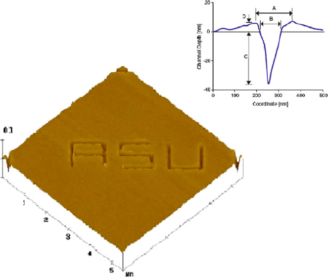
For a single pass (scan) of the ion beam, a V-shaped channel (line) is produced.
The depth profile of such a line is shown in Fig. 9.35 from Tseng [102].
The profile is notably wider than the beam diameter indicating that the energy of
scattered ions is large enough to cause sputtering. Also redeposition is evident at the
side of the line-depth profile. For precision pattern formation both sputtering and
Fig. 9.35 AFM image of FIB single-line scan and associated height profile scan (Reprinted with
permission from [102], copyright 2004, American Vacuum Society)
710 D.R. Hines et al.
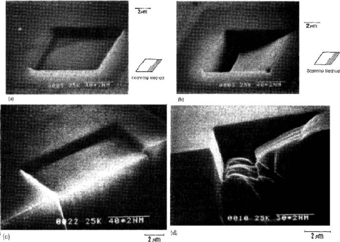
Fig. 9.36 FIB profile after single and multiple scans with the same total dose (Reprinted with
permission from [103])
redeposition must be controlled. For many features in nano- and microfabrication,
it is desirable to have vertical sidewall profiles and flat-bottomed features with high
aspect ratios. To obtain most types of desired patterns with FIB, multiple passes
must be performed. As shown in Fig. 9.36, multiple scans can lead to better feature
profiles. Figure 9.36a, b were fabricated using the same total exposure time: for (a)
a single pass was performed at 5 µm/s whereas for (b) 200 passes were performed
at 1 mm/s. The total dose rate was the same for both cases (1.9 × 10
18
ions/cm
2
)but
the single-pass feature shows an inclined bottom due to redeposition (keep in mind
that for some applications such a feature profile may have advantages).
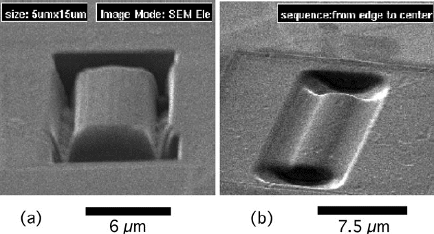
Because of the dynamics of redeposition, different scanning histories can pro-
duce dramatically different features. For example, Fig. 9.37 shows the difference
between scanning from edge-to-center as opposed to scanning from center-to-edge.
Review papers covering FIB and associated uses of these tools can be found in [100,
104–117].
9.5.3 Gas-Assisted Electron and Ion Beam Lithography
With the introduction of a precursor gas, both electron and ion beams can be used
to perform either material removal or deposition. The removal process here is beam
induced etching rather than sputtering as was presented above. For electron beam
9 MEMS Lithography and Micromachining Techniques 711
Fig. 9.37 FIB feature resulting in scanning from (a) center-to-edge and from (b) edge-to-center
(Reprinted with permission from [118])
induced etching, the etching process is initiated by an excitation/dissociation of
molecules in the precursor gas. The resulting gas molecules can then chemically
react with atoms on the surface of the substrate forming volatile molecules contain-
ing substrate atoms that are easily removed in vacuum [119]. Precursor gases can
also be added to an ion beam to combine the affect of etching and sputtering.
In addition to gas-assisted milling, electron and ion beams can also be used to
perform gas-assisted deposition of materials [119, 120]. An example of a similar
process is often observed in SEMs with the formation of thin-films resulting from
contamination after the electron beam has scanned over a specific area on the surface
of a sample. Silicone vacuum pump oil was deliberately used to form a polymer
film on a substrate in an SEM as one of the first demonstrations of this technique
[121, 122]. More recently the process of electron-beam-induced deposition has been
exploited to deposit other desired materials [123–125]. van Dorp and Hagen [126]
list more than a dozen materials and precursor gases that have been used for gas-
assisted e-beam deposition. A compelling example of e-beam-induced deposition is
illustrated using a tungsten precursor gas to fabricate a nanoscale map of the world
onaSi
3
N
4
substrate. The map is 230 nm across and contains height variations that
represent mountain ranges around the world [127].
9.5.4 Dip-Pen Lithography (DPN)
Dip-pen lithography is an extension of scanning probe microscopy and atomic force
microscopy (AFM). Instead of imaging a surface with a probe tip, the probe tip is
used to deliver an “ink” to the substrate surface. An AFM tip is coated with an ink,
and then when brought into proximity to a surface, a meniscus is formed between the
712 D.R. Hines et al.
tip and surface. As the tip is moved with respect to the surface, ink is pulled off the
tip (due to surface tension) and remains on the surface. In this way, sub-50 nm lines
of material can be deposited either sequentially or in parallel (using multiple tips).
Possible inks include small organic molecules, polymers, DNA, proteins, peptides,
colloidal nanoparticles, metal ions, and sols. Both hard and soft substrate materials
can be patterned, including insulating, semiconducting, and metallic substrates. The
process of writing dots and lines is dependent on parameters such as temperature,
humidity, writing speed, and contact force between tip and substrate, in addition to
the physical and chemical properties of both the ink and substrate materials.
Biological samples are also possible with these schemes, rhodamine 6G (R6G)
being a good example [128]. An ultrasharp Si
3
N
4
tip was dipped into a 2 × 10
−5
M
solution of R6G for 30 s and then dried in N
2
gas. The pattern was then written on a
mica substrate in a 23
◦
C and 36% humidity air environment. The feature was written
at both 0.01 and 0.04 µm/s. In this case, the 0.01 µm/s drawn feature generated a
smooth and continuous line, whereas the 0.04 µm/s case produced a discontinuous
line.
For the writing of chemical materials, DPN can be used to deposit nanometer-size
features comprised of self-assembled monolayers (SAM). For example, high-
resolution patterns of octadecanethiol (OTS) molecules on an Au film [129] and
hexamethyldisilazane (HMDS) molecules on either a Si or a GaAs substrate [130]
can be fabricated. Such SAMs can be used to fabricate high-resolution hydropho-
bic/hydrophilic patterns or chemical etch barriers for further processing. Zhang et al.
[131] demonstrated DPN by writing 16-mercaptohexadecanoic acid (MHA) features
onto a Au-coated Si substrate. The MHA pattern was used as a wet chemistry etch
mask for the Au film and then the patterned Au layer was subsequently used as a
reactive ion etch (RIE) mask for the Si.
9.5.5 Direct-Write Laser
Since their advent, the interaction of laser beams with materials has been of prime
interest. Any laser process that modifies, adds, or removes material from a substrate
can be thought of as a form of direct-write laser lithography. This is a maskless
technique that scans the laser beam from point to point. This can allow for a one-
step process that does not need a resist layer, backing, or wet chemistry. It is also not
restricted to 2-D processing on flat surfaces. The laser beam and/or substrate can be
moved in x, y,orz in a manner that can produce a 3-D feature of arbitrary shape. This
can also be performed on arbitrary-shaped substrate surfaces not only flat wafers.
Inasmuch as the laser beam can be programmed to raster in any desirable way,
the need to design and fabricate new or multiple mask sets in eliminated. Several
main components are needed: (1) laser source, (2) optics to shape and deliver the
laser bean to a desired location, (3) substrate mount, and (4) r elative translation
between laser and substrate. Three main classes of laser direct-write lithography
can be enumerated: subtractive, additive, and modification.
9 MEMS Lithography and Micromachining Techniques 713
The subtractive mode typically involves photochemical, photothermal, or photo-
physical processes [132] of which ablation, surface cleaning, milling, and drilling
are examples. The modification mode typically involves thermal methods causing a
chemical or structural change. For example, thermally induced phase change from
crystalline to amorphous, sintering, and changes in solubility (similar to UV expo-
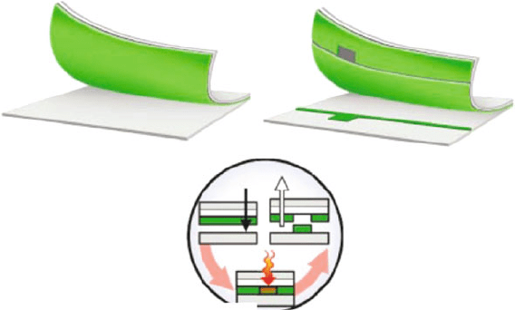
sure in photolithography but on a point-by-point processing). The addition mode
typically involves the transfer of material from one substrate to a second substrate.
For example, a bilayer film on a transparent substrate where the bottom layer is
vaporized by the laser beam thus tearing off the top layer which is then propelled
across the gap to be deposited onto the second substrate. The additive process is
illustrated in Fig. 9.38 and has been used to fabricate a thin-film transistor (TFT) by
Blanchet et al. [133].
Fig. 9.38 Illustration of the direct-writing laser additive process to transfer one material onto a
second substrate (Reprinted with permission from [133], copyright 2003, American Institution of
Physics)
Laser-induced chemical-vapor deposition (LCVD) is an example of the modi-
fication method [134] that can be used to form 3-D structures on a substrate. The
substrate is surrounded by material in the gas phase and the laser beam is focused to
the desired location to induce a chemical reaction t o change the gas into a solid form.
The laser beam is moved around to create the desired structure [135]. Two types of
reactions are generally used, either decomposition reactions or combination reac-
tions. These reactions can be either photolytic or pyrolytic. Duty et al. [135] list
materials that have been deposited using pyrolytic methods. The list includes metals
such as Al, Cu, and Au; semiconductors such as Si and Ge; and ceramics such as
Si
x
N
y
, SiC, and TiN. The list also includes starting reagents along with various pro-
cessing parameters. Figure 9.39 illustrates the LCVD process where a laser beam is
depicted to induce a chemical reaction to convert a gas or liquid phase into a solid as
