Ghodssi R., Lin P., MEMS Materials and Processes Handbook
Подождите немного. Документ загружается.

694 D.R. Hines et al.
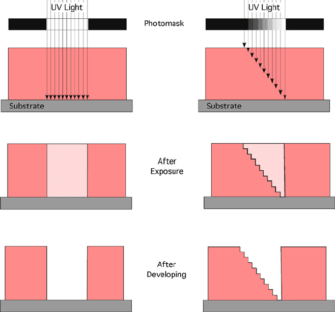
Fig. 9.22 Comparison between photoresist exposure profile using standard and grayscale pho-
tomasks (Modified from [63], reprinted with permission)
been written for these photomasks. These masks can also be used in both projection
and contact lithography systems, which makes them more versatile when consider-
ing equipment availability and differing cleanroom capabilities. The cost of HEBS
masks can also be up to one order of magnitude more than standard chrome on
quartz plates, which has significantly limited the wide adoption of this technique in
the MEMS community. However, when an extremely smooth 3-D profile is required,
or contact lithography is the only option available, HEBS glass is an excellent choice
for grayscale lithography. HEBS glass is often used for lenses and high-density lens
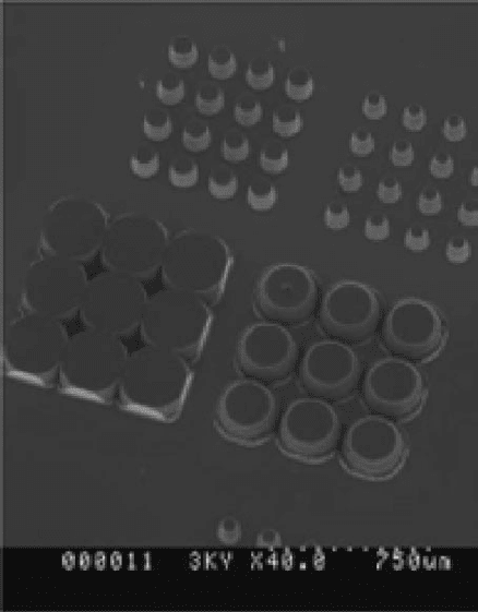
arrays due to the smoothness achieved in the final photoresist profile. Figure 9.23
shows an example of patterned silicon structures using HEBS glass lithography.
As already mentioned, HEBS glass masks are fabricated using an electron beam
to initiate the chemical reduction of the silver-containing doped glass. The opacity
of the mask is determined by the electron beam parameters with the dose prac-
tically controlled by changing the dwell time and the energy of the beams. The
9 MEMS Lithography and Micromachining Techniques 695
Fig. 9.23 Silicon profile
generated using a HEBS glass
mask and DRIE etching
(Reprinted with permission,
Lawrence Livermore National
Laboratory, https://www-eng.
llnl.gov/mic_nano/
mic_nano_MEMS.html)
ability to fine-tune the dose allows for a very large number of gray levels, over
500 for most cases. Unlike a chrome mask, however, the dark areas of the mask
never become 100% opaque. Fabrication of a mask is performed exclusively through
Canyon Materials, Inc. (CMI) who provide detailed instructions of how to struc-
ture the mask design file for them to perform the electron beam exposure of the
mask. Inasmuch as many processing variations exist for the photoresists and opti-
cal lithography sources, CMI provides standardized calibration masks to establish
proper photoresist exposure times, thicknesses, and development procedures. There
are a number of publications available showcasing the capabilities of these masks
[64–66].
There is another commonly used method that has been more widely adopted,
utilizing a variable transmission mask just like the HEBS glass, but with standard
mask fabrication techniques. This is accomplished by pixelating the chrome pat-
terns on the masks so as to control the amount of light transmitted. This technique
necessitates the use of a stepper lithography system, which can be a problem if such
a system is not readily available. As discussed below, the limitations on pixelation
result in a finite number of transmission steps (called gray levels) between 0 and
100% transmission. For the photoresist, both sensitivity to UV light exposure and

696 D.R. Hines et al.
selectivity to the subsequent substrate etching will be important for utilizing all the
gray levels. For example, if the photoresist is too sensitive to UV light, light from
the first grayscale level will fully expose the photoresist at the substrate surface
before light from the last grayscale level has a chance to expose the top surface
of the photoresist. If the photoresist is removed too fast during the substrate etch
then the photoresist will be consumed before the desired etch depth can be reached.
Likewise, if the photoresist is not consumed at all then none of the grayscale levels
can be transferred into the substrate etch.
9.3.1 Photomask Pixelation
To establish partial transmission of UV light during the exposure step in the pho-
tolithographic process, the opaque part of the photomask can be pixelated as shown
in Fig. 9.24. The pixels need to be designed so that they modulate the transmission of
UV light without being directly imaged onto the surface of the photoresist. For this
reason the pixel dimensions need to be below the diffraction limit of an optical pro-
jection s ystem. When making a particular mask design, the spacing (pitch) and the
pixel dimensions are varied to create different levels of transmission, generating the
gray levels in the photoresist pattern. In this way, the minimum dimensions available
in the design of a pixelated gray mask are limited by the projection lithography sys-
tem’s resolving power, and the resolution of the mask writing system. In addition,
less pattern control is available when making complex 3-D structures inasmuch as
pixel size and pixel spacing are all different based upon the particular transmission
or gray level being expressed. Minimum dimensions for singular gray levels are then
fixed by this pixel size and pitch limitation. Pixelated grayscale masks are in gen-
eral best suited for larger patterns, or for situations where mask cost is a restrictive
parameter. A more detailed discussion of the mask design and pixelation is included
in the case study section of this chapter (Case Study 10).
Pixels
Pitch
Pixel ArrayMask
Fig. 9.24 Pixelation of a gray-scale photomask (Reprinted with permission from [67])
9 MEMS Lithography and Micromachining Techniques 697
9.3.2 Photoresist Properties for Grayscale Lithography
9.3.2.1 Contrast and Thickness
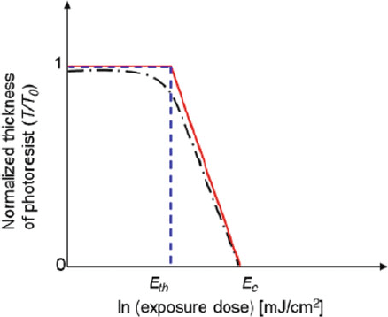
A photoresist contrast curve is shown in Fig. 9.25, with thickness plotted as a func-
tion of the logarithm of the UV light exposure. Two exposure points are noted: E
th
is the minimum exposure required for the photoresist to react to light and E
c
is the
minimum exposure required to completely remove (or clear) the photoresist from
the substrate surface [68]. The linear slope between these two exposure points is
defined as the “contrast.” A larger photoresist contrast translates to a smaller dif-
ference between the two exposure endpoints and to a smaller processing window.
For grayscale lithography, larger processing windows are desirable so that good
differentiation between exposure levels can be realized. Therefore, low-contrast
photoresists are typically used for grayscale lithography.
Fig. 9.25 UV light exposure
profile as a function of
photoresist thickness
(Reprinted with permission
from [68], copyright 2008,
American Institute of
Physics)
In addition to contrast, the thickness of the photoresist layer is also important.
The thickness should be chosen so that E
th
is the exposure produced by the largest
grayscale level and that it occurs at the top of the photoresist surface precisely when
E
c
is the exposure produced by the smallest grayscale level.
9.3.2.2 Exposure and Developing Times
The exposure time is determined as the time needed to deliver an exposure equal to
E
c
. Theoretically, determining the exposure time is straightforward but in practice
it can be problematic. Temperature, humidity, variations in photoresist thickness,
intensity fluctuations of the stepper, and so on can all affect both the exposure and
the developing time. Therefore, it is typical to empirically determine these times by
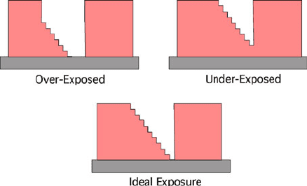
performing test exposures using a calibrated mask. Overexposing or underexposing
will leave a thickness bias on the whole photoresist structure that will interfere with
698 D.R. Hines et al.
Fig. 9.26 UV exposure
levels for gray-scale
lithography (Modified from
[67], reprinted with
permission)
the proper transfer into the substrate beneath, creating a disparity in the final device
thickness, as illustrated in Fig. 9.26.
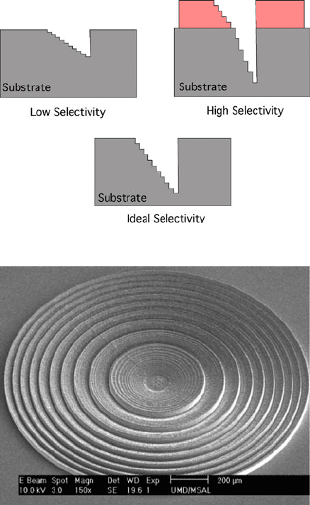
9.3.2.3 Etch Selectivity
Photoresist etch selectivity is defined as the ratio of the substrate etch rate to the
photoresist etch rate for a given set of etching conditions. A high etch selectivity
is usually desirable for standard photolithography applications where the original
fidelity of the photoresist pattern is designed to survive the substrate etch, thus pro-
ducing a perfect replica of the photoresist pattern etched into the surface of the
substrate. For grayscale lithography, the photoresist layer is designed to be con-
sumed during the substrate etch. Often times varying levels of O
2
gas are introduced
during the etch to speed up the photoresist consumption rate. Using this method, it is
easier to fine-tune the resulting selectivity rate. The resulting pattern etched into the
substrate reflects the thickness profile of the original photoresist pattern. Each gray
level developed into the photoresist corresponds to a specific etch depth into the sub-
strate surface which is determined by the etch selectivity and the starting thickness
of the patterned photoresist layer. The difference in final structure transfer is illus-
trated in Fig. 9.27 . Photoresist thicknesses of 6–10 µm, when combined with etch
selectivity between 40 and 100, translate into substrate etch depths ranging from
tens to hundreds of micrometers. An example of a fully transferred pattern using
HEBS glass has already been shown above (Fig. 9.24), and a typical transferred pat-
tern using a pixelated mask is shown in Fig. 9.28. More detailed discussion of the
silicon etching process is given in Chapter 7.
9.4 X-Ray Lithography
X-ray lithography was originally developed as an attempt to achieve smaller device
geometries by using the very short wavelength of X-rays (∼0.7–1 nm optimally), the
ability to have highly collimated X-ray sources, and the relatively s mall scattering
9 MEMS Lithography and Micromachining Techniques 699
Fig. 9.27 Etch selectivity
profiles for gray-scale
lithography (Modified from
[67], reprinted with
permission)
Fig. 9.28 Silicon Fresnel
lens patterned using a
pixelated grayscale mask and
etched using DRIE
(Reprinted with permission
from [69])
of X-rays through common materials. Theoretically, 20 nm resolution features can
be defined, but in practice it is more common to see features in the 50 nm range [70].
This is due to a number of challenges encountered in the lithography process, such
as synchrotron X-ray wavelength spectral broadening, mask–substrate distance, and
mask distortions [71].
X-ray lithography follows a very similar process to that of UV lithography: a
pattern is transferred into an optically sensitive resist material (in this case X-ray
sensitive resist) by illumination through a mask onto the resist. Although there was
an initial interest in X-ray lithography for VLSI design, most X-ray lithography is
used today for the fabrication of high-aspect-ratio molds in a process commonly
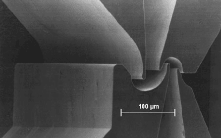
referred to as LIGA (Lithographie, Galvanoformung, Abformung)[72]. LIGA was
initially used in the fabrication of nozzles for uranium enrichment (Fig. 9.29), with
700 D.R. Hines et al.
Fig. 9.29 LIGA-fabricated
uranium enrichment nozzle
(Reprinted with permission
from [73])
many other applications being developed after the initial demonstration of this tech-
nology [73]. LIGA takes advantage of the very high aspect ratios (100:1) achievable
through X-ray lithography and uses the resulting polymer resist structures as molds
for electroplating (metals), or other molding processes. There have also been exam-
ples of SLIGA performed which incorporates sacrificial layers into the standard
LIGA process thus allowing for the creation of freestanding and moveable struc-
tures directly on the substrate [74]. X-ray lithography is used in MEMS processes
and devices primarily in this context [75, 76].
The primary challenge for X-ray lithography is in the required light sources for
highly collimated X-ray beams. These types of sources are generally much more
complex than the typical UV discharge lamps used in UV lithography. In addition,
due to their very high energy, X-rays cannot be focused and guided using tradi-
tional lenses and mirrors as in UV lithography. The synchrotron is one of the most
important enabling tools of high-aspect-ratio X-ray lithography, capable of emitting
high-power, highly collimated radiation. This high collimation permits relatively
large distances between the mask and the substrate without the penumbral blurring
that occurs from other X-ray sources, and also enables the high aspect ratios in
exposed photoresist, which is beneficial to the development of LIGA.
In the electron storage ring or synchrotron, electrons follow a circular path. The
radial acceleration of the electrons causes electromagnetic radiation to be emitted
forward. The radiation is thus strongly collimated in the forward direction of the
moving electrons and is essentially parallel. These radiation sources also provide
higher flux densities, which enable shorter exposure times. Photon energies for a
LIGA exposure are approximately distributed between 2.5 and 15 keV.
9.4.1 X-Ray Masks
X-ray masks are one of the bottlenecks in the commercial development of LIGA
and X-ray lithography [77], because there are a number of materials used for
this process, depending on the particular research group’s fabrication facilities and
9 MEMS Lithography and Micromachining Techniques 701
capabilities. The general concept employed in X-ray mask generation is to have
a highly transparent material for the field of the mask (low-Z materials), and an
X-ray-absorbent material to define the features on the mask (high-Z materials). This
is commonly done with a substrate material of graphite or vitreous carbon, or some-
times silicon nitride, silicon carbide, or diamond membranes [78, 79]. The latter
are not as readily preferred as the membranes required for the masks in these cases
are very fragile. Beryllium substrates are very attractive mask materials due to their
very high X-ray transparency and the ability to make them much thicker and more
stable as compared to membrane approaches. The patterned absorbing features are
typically X-ray absorbing metals such as tin, copper, gold, or lead [76].
One of the challenges to making these large area masks is the ability to maintain
low distortion in the finalized masking image. Due to the 1:1 mask transfer, the accu-
racy of the mask features is paramount in importance. These distortions are caused
by a number of factors, with a major one being film stresses in the membrane materi-
als. More masks are being made out of SiC due to this distortion issue. Research has
also been undertaken in an attempt to predict these distortions and counteract them
with the design of the mask itself, similar to what occurs in ultra-high-resolution
masks for UV lithography. Even the mounting of the mask contributes to distor-
tions in the mask pattern due to stresses; most masks are mounted in metal rings to
prevent some of these adverse effects.
The definition of the mask features can be done a number of ways and greatly
depends on the required resolution of the mask patterns. Direct-write methods such
as electron beam lithography are used to achieve the most accurate features for the
mask, but this carries the disadvantage of being very time consuming for the large-
area masks in X-ray lithography. Other methods (such as described in this chapter)
are also employed to pattern the X-ray masks with their own varying lithographic
tolerances.
Fabrication of these masks is often quite involved, in an attempt to reduce film
stresses and achieve high-resolution features. Typically, the mask fabrication begins
with a silicon wafer that is coated with the membrane material (silicon nitride, sili-
con carbide). Two methods are commonly used to pattern the mask absorber metal
(tungsten, titanium, gold, etc.). The metal can be blanket deposited on the back-
side of this coated wafer, and then patterned using subtractive processes (dry or wet
etching). Other methods employ thicker photoresists and rely on additive processes
such as plating to deposit a thicker absorber coating which is required for lower
Z materials such as gold to achieve good exposure contrast. This can be done a
number of ways, one of which involves performing an X-ray lithography step on a
thinner coating of X-ray photoresist to f orm a plating mold for the final mask, but
can be performed with normal thick photoresist plating mold technologies as well.
The thickness of this absorbing pattern can vary from a few microns to up to 50 µm,
and depends on the thickness of the photoresist to be exposed, both of which are
directly related to the required X-ray energy [76].
The completed mask is normally placed in a glass or metal ring at this point
in the process to provide the wafer with stability and strength. After this step, the
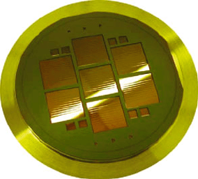
membrane is released by backside etching of the silicon wafer. A photograph of a
finalized X-ray mask is shown in Fig. 9.30.
702 D.R. Hines et al.
Fig. 9.30 An example of an
X-ray mask made from SiC
(Reprinted with permission
from [80])
9.4.2 X-Ray Photoresists
X-ray photoresists function very similarly to the resists used in e-beam lithography
(see Section 9.5.1), and thus most e-beam resists can be used for X-ray lithography;
poly(methyl methacrylate) (PMMA) is most commonly used for X-ray lithography,
however, SU-8 is also a possible choice [81]. PMMA is exposed through the gen-
eration of Auger and photo electrons by the X-rays entering the photoresist. These
interactions chemically alter the resist polymer chains through scission, reducing
their order from approximately 1,000,000 to 1000. This is what allows the polymer
to be dissolved by developers that attack the lower-order polymer chains [82].
Photoresists used in X-ray lithography for MEMS applications are generally
applied in thick layers to take advantage of the high aspect ratios achievable, par-
ticularly for LIGA. The typical choice PMMA is applied to the substrate for some
of the thinner applications by way of spinning, or more probably by a glue-down
process in which a precast sheet of PMMA is attached to the substrate material
[82]. This second option allows for much thicker molding layers and also prevents
the buildup of stress which can be caused by casting the photoresist directly on the
substrates. The PMMA is then milled down to the precise height before X-ray expo-
sure. In some cases, after exposure a second PMMA layer is glued to the surface for
a second exposure, facilitating the creation of even higher aspect ratios [83].
In the case of ultra-high- and very-high-resolution X-ray lithography, the thick-
ness of the photoresist is somewhat limited, with thicknesses of typically 5–50 µm.
These thicknesses have been found to be the threshold for adverse optical effects
such as diffraction and scattering which occur because of mask dimensions and
X-ray energy, respectively [84].
9.4.3 Exposure
Due to the fragility of X-ray masks fabricated on thin membranes, contact lithogra-
phy is not possible without damaging the masks. In addition, the high energy of the
9 MEMS Lithography and Micromachining Techniques 703
X-rays prevents the use of a typical projection lithography system where patterns
can be focused onto the surface of the substrate and reduced in scale. As neces-
sitated by these conditions, all X-ray masks must be 1:1. Instead of using these
more common lithographic techniques (projection and contact), proximity masking
is used. Divergence and near-field diffraction commonly encountered in traditional
proximity UV lithography are not as large a problem for X-ray lithography due to
the highly collimated radiation and the very small wavelength of the X-rays. Mask-
wafer spacing of anywhere from 5 to 50 µm i s typical and varies depending on the
available equipment or the required resolution, as increasing this gap does have a
negative effect on the final patterns [70, 82–84].
Exposure times and energies vary greatly based upon the thickness of the pho-
toresist used and the required critical dimension size. X-ray energies for exposure of
high-resolution patterns are typically around 1 keV, whereas a more typical MEMS
application will require X-ray energies of 5–15 keV. A typical dose for PMMA is
4–20 kJ/cm
3
. Anything higher than this could possibly cause the resist to burn [85].
Exposure times vary, again, based upon the thickness of the resist, but generally are
no more than a few hours. Care must be taken not to perform very long exposures
to prevent mask and substrate heating due to the X-ray exposure, which can cause
misalignment and mask distortions [86]. The time of the exposure plays a large part
in the choice of the masking material used.
Karl Suss has created a commercially oriented X-ray stepper tool that allows a
pattern to be exposed using X-ray lithography [71, 87, 88]. This particular device
operates with a proximity gap of 20–50 µm, and has a scanning speed of 0.5–
20 mm/s. In the literature, custom modifications to this tool have yielded very small
proximity gaps to approximately 10 µm[70]. The tool still requires a separate
synchrotron radiation source, however. The stepper functions similarly to that of
a standard stepper and can align masks to each other via CCD cameras to facilitate
multilevel X-ray exposures with high pattern alignment accuracy.
9.4.4 Development
For high-aspect-ratio structures the resist–developer system usually has a ratio of
dissolution rates in the exposed and unexposed areas of 1000:1. Developers vary:
GG developer (composed of diethothxy and morpholine) is sometimes used [82];
another standard developer used is a mixture of tetrahydro-1,4-oxazine (20%),
2-aminoethanol-1 (5%), 2-(2-butoxyethoxy)ethanol (60%), and water (15%) [89].
The former provides nearly 100% selectivity and does not induce any additional
stresses or cracks in the exposed resist. Developers vary on a case-by-case basis and
are usually empirically standardized and characterized.
After development, the substrate is rinsed with deionized water and dried either
in a vacuum or by spinning. At this stage, the PMMA structures can be released
as the final product or can be used as molds for subsequent metal deposition. An
illustration of the complete process is shown in Fig. 9.31. Discussion of the plating
