Ghodssi R., Lin P., MEMS Materials and Processes Handbook
Подождите немного. Документ загружается.

764 A.D. Raisanen
described by a partially filled set of electronic states. One can define an energy ref-
erence called the Fermi level, denoted E
F
, which designates the energy at which the
probability of the states at that energy being occupied is 0.5. At absolute zero, this
implies the states above E
F
are empty and the states below E
F
are filled, but at finite
temperatures there is a tailing off of occupied states towards higher energy leading
to a distribution of occupied and unoccupied states centered at the Fermi level.
The vacuum level E
vac
is the energy above which an electron is no longer bound
to the solid; that is, it becomes a free electron in space. The difference between the
vacuum level E
vac
and the Fermi level E
F
is known as the work function Φ of the
metal. In the semiconductor, we have a conduction band edge at E
C
, above which
electrons are free to move as carriers under the influence of an electric field, and a
valence band edge E
V
, below which holes can move as carriers. The semiconduc-
tor also has a well-defined Fermi level E
F
, where the probability of an electronic
state being occupied is 0.5. In the example illustrated, the semiconductor is n-type,
because E
F
is close to E
C
implying the presence of carriers in the conduction band.
The energy difference between the conduction band and the vacuum level in the
semiconductor is called the electron affinity χ , which is analogous to the metal’s
work function.
When the metal and semiconductor are brought together, charge will move from
one side to the other until the Fermi levels align on both sides. This charge redistri-
bution makes one side slightly positive and the other side slightly negative, inducing
a built-in electric field at the junction. This electric field alters the electronic struc-
ture of the semiconductor as shown in Fig. 10.9b, a phenomenon known as band
bending. The discontinuity between the semiconductor conduction band (in the n-
type semiconductor example shown here) and the metal Fermi level produces a
barrier against electronic transport across the boundary. This discontinuity, called
the Schottky barrier
B
has a height equal to the difference between the metal Fermi
level and the s emiconductor electron affinity. The band bending area is called the
depletion region, where electrons in the example illustrated have transferred into
the metal. Similar diagrams can be generated for p-type semiconductors [ 5], where
holes diffuse into the metal and the discontinuity is between the metal Fermi level
and the valence band of the semiconductor. The width of this depletion region is
determined by the doping level of the semiconductor, with higher doping levels
producing narrower depletion regions.
The presence of a Schottky barrier at a metal–semiconductor interface has pro-
found implications for electron transport through these junctions. In essence, a
significant barrier height produces a rectifying junction with electrical properties
similar to a diode, allowing easy current flow in only one direction. Some elec-
tronic devices make explicit use of this phenomenon, but it is typically undesirable
for making good electrical contacts with predictable bidirectional current flow
properties. See Fig. 10.9.
In principle, matching a metal work function with a semiconductor electron affin-
ity would eliminate this barrier entirely, but in practice this does not work in most
cases due to the presence of defect states at the interface, metal–semiconductor
intermetallic phase formation, or other complicating factors [ 16]. The technique
10 Doping Processes for MEMS 765
employed by most workers is to dope the semiconductor, or at least the surface
region of the semiconductor, to a high level, resulting in a very narrow depletion
width (<100 nm). Even if the actual Schottky barrier height is quite large, electrons
and holes can simply tunnel through the narrow barrier, enabling low-resistance cur-
rent transport in either direction [5]. Doping densities of 1×10
18
cm
−3
or better are
common for contact formation applications. Simple aluminum contacts on doped
silicon are most common in the MEMS world, but specific contact metallurgies and
doping strategies are usually required to create good ohmic contacts for different
semiconductors [17].
10.2.2 Etch Stop Techniques
Although dopant processes in semiconductors are most commonly used for pro-
ducing electrically active devices, dopants also have an important role in bulk
micromachining fabrication sequences. Modification of the dopant concentration
in silicon and other semiconductors has the useful effect of altering the etch rate of
the semiconductor matrix in specific etchants. This effect can be employed as a rea-
sonably accurate etch stop for fabrication of t hin unsupported membranes or other
structures, and forms the basis for a variety of electrochemical etch techniques.
Silicon can be etched with a number of wet chemical etches, including mixtures
of hydrofluoric (HF), nitric (HNO
3
), and acetic (CH
3
COOH) acids [18], heated mix-
tures of ethylene diamine (C
2
H
4
(NH
2
)
2
), pyrocatechol (C
6
H
4
(OH)
2
), and water
[19], tetramethyl ammonium hydroxide ((CH
3
)
4
NOH) [20], and solutions of hot
potassium hydroxide (KOH) and water [21]. All of these commonly used silicon
etches are significantly sensitive to the doping level of the silicon material being
etched.
Hydrofluoric acid, nitric acid, and acetic acid (HNA) constitute a common wet
isotropic etch solution for silicon and polysilicon, with typical etch rates of a few
microns per minute. It is possible to use standard photoresist films to mask this
etchant for s hort times, although the resist is attacked by the strong oxidizer HNO
3
and the interface between silicon and the photoresist is often attacked during etches
of more than a few microns causing film peeling and pattern failure. Silicon diox-
ide, silicon nitride, and sometimes gold are used as etch masks for deeper etches.
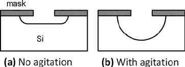
The HNA etch chemistry can be difficult to use reproducibly because the etch
rate, selectivity, and even etch profile (Fig. 10.10) depend on the chemical mixture
Fig. 10.10 Isotropic HNA
etch profiles generated (a)
without solution agitation, (b)
with solution agitation
766 A.D. Raisanen
composition and age, agitation, and doping of the silicon material itself. Defects in
the silicon can also affect the etch significantly, and many workers use the HNA etch
and variants to “decorate” and delineate various crystal defects.
Models of the mechanism by which HNA etches silicon involve injection of holes
to increase the oxidation s tate of the silicon atoms, enabling attachment of hydroxyl
groups (OH
−
)[22]. The oxidized silicon then reacts with the HF in the solution
to produce soluble hexafluorosilicic (H
2
SiF
6
) species, which dissolve in the solu-
tion. The key factor that makes these etches interesting from a doping perspective
is the necessity for hole injection to initiate the etch, rendering this etch susceptible
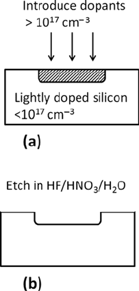
to changes in doping concentration of the material being etched. With the correct
etchant concentration, silicon doped in excess of 10
17
cm
−3
of either n- or p-type
will be etched rapidly, whereas silicon with a lighter doping level will be etched
more slowly [23]. This differential etch rate can be utilized in MEMS fabrication
for producing channels, releasing membranes, and other three-dimensional struc-
tures. Many workers attempting these etch processes have encountered significant
difficulties in reproducing exact results found in the literature, as etch results tend
to be sensitive to low levels of chemical contaminants, roughness of the silicon
surface, presence of defects, and other minor variables [24]. Specific process rec-
ommendations are given in the process selection guide following this section. See
Fig. 10.11.
In contrast to the isotropic HNA wet chemical etch, ethylenediamine/
pyrocatechol (EDP), TMAH, and KOH etches are highly anisotropic; that is, they
have very different etch rates in different crystallographic directions within the sil-
icon crystal. This effect can be used to produce geometrically faceted structures,
self-limited channel etches, nozzles, and controlled undercuts or release etches with
a minimum of masking steps [12].
Fig. 10.11 Dopant-
dependent etch stop
procedure for isotropic HNA
etch. Lightly doped silicon is
not etched, whereas heavily
doped material is dissolved
10 Doping Processes for MEMS 767
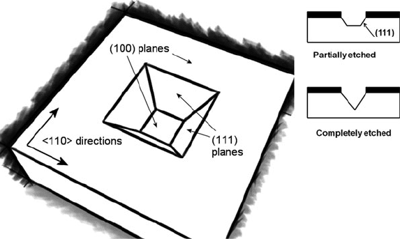
Fig. 10.12 Geometry of silicon orientation-dependent etch processes
Figure 10.12 illustrates one of the most common geometric arrangements used
by MEMS researchers, with a (100) surface plane wafer covered by a mask with
a square hole in it oriented along <110> directions. The masking material is usu-
ally silicon nitride, although silicon dioxide can be used for relatively short etches
as it is slowly attacked, by KOH in particular. When exposed to the anisotropic
etch chemistries, the (100) planes etch rapidly, and the (111) planes etch relatively
slowly. A geometric structure is revealed composed of (111) planes, which forms a
pyramidal etch pit terminating in a point if it is allowed to etch to completion.
One of the useful features of this type of etch is its self-limiting behavior; timing
is not critical as etching essentially stops once (111) planes are all that remain. Long
v-shaped grooves can be fabricated by opening long slots in the mask, and the depth
of the grooves will be determined by the width of the slot. Holes for vias or nozzles
can be etched right through the entire silicon wafer by making certain that the mask
opening is large enough to prevent the (111) planes from coming to a point before
the wafer is etched completely through.
The atomic density of each crystal plane is regarded as the origin of the etch rate
anisotropy [25]. The (111) plane in silicon has the highest atomic packing density
and lowest number of dangling bonds per unit area, and is therefore the slowest
etching plane. Other plane etch rates vary according to their relative atomic packing
densities and bond densities. The mechanism of etching in these alkaline solutions
is believed to involve injection of electrons during Si reaction with hydroxyl ions
in the solution, which enables dissociation of water molecules and production of
hydrogen and silicates Si(OH)
6
2−
[21]. The silicates are then complexed by the
etch solution forming soluble silicon-containing species. Dangling bond densities,
as well as formation of a screening boundary layer of water molecules at the surface,
both of which vary according to the crystal plane exposed, are also believed to play
a role in setting the anisotropic etch rates observed between crystal planes.
768 A.D. Raisanen
A common structure fabricated with the anisotropic etch process is a thin
diaphragm made of silicon, used in pressure sensors and various transducers. If
the etch rate and wafer thickness are known, it is possible to time the etch and
remove a wafer from the anisotropic etchant before etching penetrates all the way
through the silicon, leaving a thin membrane. Control of the membrane thickness
by this method is difficult, as the etch rate varies somewhat depending on solution
age, and the thickness of silicon wafers varies slightly between individual wafers.
Fortunately, the etch rate of silicon in these anisotropic etchants varies with doping
level.
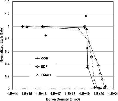
High levels of boron doping have been found to inhibit the etching of KOH [26,
27], EDP [28], and TMAH [29] anisotropic etchants, as illustrated in Fig. 10.13.
Doping densities of 1×10
19
−1 ×10
20
cm
3
or higher are required, which approach
the solid solubility limits for boron. Other dopants, such as phosphorus, or even
nondopants such as germanium are reported to exhibit this effect to a lesser degree
[28], but are more difficult to implement as etch stops due to the very high doping
densities required. Seidel [28] explains this etch stop behavior in terms of the strong
band bending produced at the silicon interface by the highly doped layer. Normally,
electrons injected into the silicon from the etch solution will be confined near the
interface due to the presence of a Schottky barrier, where they will be available to
reduce water molecules necessary to drive the reaction.
A heavily doped boron layer produces a very narrow depletion width at the inter-
face, as illustrated in Fig. 10.9c. Electrons at the surface can easily tunnel through
Fig. 10.13 Relative etching rates of boron-doped silicon (100) planes in KOH, EDP, and TMAH
anisotropic etch chemistries as a function of doping level. (KOH data from [26, 27], EDP from
[28], and TMAH from [29], used with permission)
10 Doping Processes for MEMS 769
Fig. 10.14 Boron etch stop
used to fabricate a thin
diaphragm in (100) silicon
using anisotropic etchant
this narrow depletion region and diffuse into the crystal bulk, starving the surface
silicon oxidation reaction and stopping the etch.
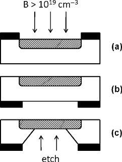
To fabricate a structure such as a thin silicon diaphragm, a process like the one
schematically illustrated in Fig. 10.14 is used. The f ront surface of a wafer is heavily
doped by boron, with the depth of the doped layer selected by the desired thick-
ness of the final diaphragm structure. The wafer is then etched from the backside
through an opening designed to fit the desired lateral size of the final diaphragm
structure. The etch proceeds until the heavily boron doped region is encountered,
at which point the etch rate decreases by one to three orders of magnitude. The
etch rate decrease makes it relatively easy to remove the wafer from the etchant
before the diaphragm is penetrated, and allows good control of final diaphragm
thickness. The very high doping density, however, makes integration of this process
with conventional CMOS electronics difficult.
Transistors are difficult to fabricate with high substrate doping levels, and high
boron concentration produces mechanical stress and defects in the silicon that
compromise electronic performance [30]. In addition, boron can outdiffuse during
high-temperature processing steps, producing undesired doping in other parts of the
chip. Deposition of a lightly doped silicon epilayer on the boron doped layer can be
used to overcome this issue in some cases.
The dependence of silicon etch rate on doping, and more fundamentally on the
transfer of electrons and holes between the surface and the etch solution, suggests
that etch rates could be controlled electrochemically by altering a potential applied
between the silicon surface and the etch solution. A number of electrochemical etch
stop arrangements have been developed [30–32] that allow very precise control of
etching without requiring the extreme doping densities of the conventional boron
etch stop.
An electrochemical cell schematically illustrated in Fig. 10.15 is configured to
allow application of an electrical potential between the wafer to be etched and an
immersed counterelectrode. When a potential is applied between the p−n junction
and the counterelectrode, charge is able to flow across the silicon/solution barrier
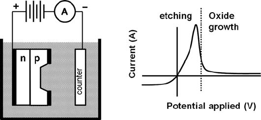
770 A.D. Raisanen
Fig. 10.15 Schematic of electrochemical etch stop process. A p–n junction immersed in an alka-
line solution is biased by an external voltage. At voltages lower than the peak current position,
silicon etches in the solution, but at higher voltages an oxide is formed, passivating the silicon
against further etching
and drive electrochemical reactions at the surface. Figure 10.15 shows a schematic
current–voltage response of silicon immersed in the etch solution, with etching
occurring below a certain critical voltage, and oxidation of the surface occurring
above that voltage. The critical voltage is found where the current flow through
the cell reaches a maximum. Above that voltage, rapid oxidation of the silicon sur-
face forms an insulating layer on the silicon, preventing any further etching from
occurring.
In the case of a p−n junction as shown, a bias can be applied such that the n-
type silicon is above the critical passivation voltage, but the voltage drop across
the reverse-biased p−n junction will result in the p-type material having a potential
low enough for etching to still occur. Thus, by operating very close to the critical
voltage, the p-type silicon can be etched by the solution, whereas any n-type silicon
that becomes exposed will form a passivating oxide, preventing further etch [30].
The electrochemical etch stop is typically utilized in the case of a p-type wafer
with an n-type epilayer or lightly doped layer on the surface, which is intended to
become a released thin membrane or other mechanical structure. Electronic com-
ponents with other doping levels can be embedded in the lightly doped n-layer at
the wafer surface, as long as there is continuous buried n-type layer surrounding
them. The doping level of the n-type layer is moderate, typically 10
15
cm
−3
or
higher, whereas the p-type layer is more heavily doped. By applying a potential to
the wafer, it is possible to alter the Schottky barrier height of the n and p regions of
the wafer, controlling charge injection and thus the rate of oxidation of the silicon
surface, which is required for the etch process. By proper selection of etch condi-
tions and applied bias, it is possible to suppress the etch rate of the n-type material
while still maintaining etch conditions on the p-type material. The p-type silicon
will undergo the usual oxidation/etch process observed for silicon in anisotropic
etchants, until the p−n boundary is reached, at which point the etch will stop. This
phenomenon allows excellent control over the etch stop condition, at the cost of
significant complications in fixturing the wafer for etching [12].

10 Doping Processes for MEMS 771
The primary difficulty is in forming a good ohmic contact to the n-type layer
on the surface of the wafer, and in protecting the wafer top surface and edges
from etchant attack while the p-type region at the back of the wafer is being
etched away. Various wafer fixturing systems made of Teflon and other polymers
are available commercially (e.g., see Advanced Micromachining Tools GmbH,
Frankenthal, Germany) to overcome this difficulty, and materials such as black wax
(e.g., Apiezon Wax W, M&I Materials, Manchester, UK) can be utilized effectively
to protect wafer surfaces as well.
In addition to the anisotropic etch processes described here, electrochemical
techniques have been utilized to implement many isotropic “porous silicon” etch
processes using hydrofluoric acid as the oxidation/etch medium [33, 34]. Silicon is
etched by striking a balance between formation and removal of an oxide layer at
the surface. This process is delicately controlled by the doping level and electrical
bias in substantially the same manner as the anisotropic etches. Some workers have
used illumination of the wafer to add yet another control mechanism to the etch
stop process [35, 36]. By illuminating the p−n junction under bias, charge may be
injected photoelectrically to drive the oxidation/etch reaction. Low doping levels are
possible using this technique, although the problems in fixturing the wafer remain
the same.
10.2.3 Materials and Process Selection Guidelines: Etch Stop
Techniques
Boron etch stop
Applicability Useful for thinning silicon wafers and producing thin unsupported diaphragms.
Can also be used to produce cantilevers, beams, and other structures in
silicon. Thickness of a diaphragm or final structure geometry can be
controlled to high accuracy by placement of boron dopant.
Implementation Generate a region of very high boron doping corresponding to the a rea to be
protected. The required doping levels are 5 × 10
19
− 1 × 10
20
boron
atoms/cm
−3
. Higher dopant densities are most effective in producing an etch
stop. Diffusion times can be substantial, doping a 10 μm t hick layer to
1 × 10
20
cm
−3
boron with solid or gas phase diffusion requires
approximately 10 h at 1100
◦
C in an inert atmosphere.
Boron layer is implemented as the top surface of a wafer, and etching proceeds
from the back. The boron-doped layer can be subsequently covered with an
epitaxial silicon layer to provide a lightly doped region for electronic
fabrication.
Wet etches are performed in a heated reflux condenser type bath. Agitation may
be added with a mechanical stirrer or N
2
bubbler, often required to prevent
solution stratification and suppress surface roughness originating from H
2
bubbles on the surface.
Thermal budget Activation of boron-doped region will generally require anneal or diffusion
temperatures >900
◦
C. Etch stop layer can be fabricated prior to other
structures requiring lower temperatures, and etch/release can be the last
processing step to avoid issues in processing thinned wafers and released
structures.

772 A.D. Raisanen
Viable etchants KOH: 10–60 wt% at 40–100
◦
C are common depending on desired etch rate
and surface roughness. In general higher KOH concentrations produce
smoother etched surfaces with lower etch rates (e.g., etch rate 140 μm/h for
25 wt% KOH versus 80 μm/min for 60 wt% KOH [21]. Some workers add
up to 20% by volume of isopropyl alcohol to improve surface roughness and
anisotropy [37]. Author’s lab uses 22 wt% KOH at 95
◦
C for routine work on
Si(100) with 190 μm/h etch rates and nearly mirror-smooth etch facets. It is
a good idea to “condition” the KOH bath by dissolving some silicon chips or
etching partway through a wafer to stabilize the etch rate, as fresh etch
solution can have anomalously high etch rates for a short time. Caution:Hot
KOH is very corrosive and can cause severe skin burns.
EDP: Many variations are possible. Some literature recipes include:
EDP type S: 1 liter ethylenediamine, 133 ml water, 160 g pyrocatechol, 6 g
pyrazine. 50–119
◦
C, etches 45 μm/h at 115
◦
C[38].
EDP type F: 1 liter ethylenediamine, 320 ml water, 320 g pyrocatechol, 6 g
pyrazine, 50–119
◦
C, etches 45 μm/h at 115
◦
C[38].
EDP type B: 1 l iter ethylenediamine, 320 ml water, 160 g pyrocatechol,
118
◦
C, etches 50 μm/h [39].
EDP type T: 1 liter ethylenediamine, 470 ml water, 176 g pyrocatechol,
etches 32 μm/h at 110
◦
C[19].
These etches tend to be sensitive to oxygen contamination and a substantial
decrease in the etch rate is observed as the solution “ages” in air. Use of an
inert gas purge is recommended. Caution: This solution is quite corrosive
and also toxic, so it should never be used without excellent containment and
ventilation.
TMAH: TMAH is extensively used in the microelectronics industry as a
photoresist developer. Solutions of 2–50 wt% TMAH in water are reported
[20, 40] with typical operating temperatures of 70–90
◦
C. Etch rate is
reduced at higher concentrations, but surface roughness obtained during etch
is decreased. Etch rates of 60 μm/h are obtained for 20 wt% TMAH in water
at 90
◦
C[40]. Caution: Solution is corrosive, but this is probably the safest to
handle of t he common anisotropic alkali etches.
Selectivity KOH: selectivities of 10–100 between boron-doped and undoped regions can
be obtained. Lower KOH concentrations result in higher selectivity [21]at
the cost of increased etch surface roughness [37].
EDP: As with KOH, selectivities of 10–100 between boron-doped and
undoped regions can be obtained. Slightly higher selectivity as a function of
doping is obtained at l ower etch temperatures, down to 66
◦
Corless[28].
TMAH: Selectivities of 10 or better can be obtained, but higher boron
concentrations are required than for KOH and EDP [29].
Material
compatibility
KOH: Etches are most compatible with Si
3
N
4
masks deposited by CVD
processes. PECVD Si
3
N
4
can be used if necessary but typically has inferior
etch resistance. SiO
2
sometimes used as a mask for short etches but it is
eroded at 10–50 Å/min depending on etch conditions. Teflon and
occasionally stainless steel are normally used for wafer fixturing. Potassium
contamination is incompatible with microelectronics, requiring a 1:1:1
H
2
O/HCl/H
2
O
2
decontamination etch before further processing. Caution:
Solution is exothermic when mixed and should be used hot.

10 Doping Processes for MEMS 773
EDP: Etches are most compatible with Si
3
N
4
masks deposited by CVD
processes. SiO
2
sometimes used as a mask for moderate etches but it is eroded
at 1–10 Å/min. Some metals including Ta, Au, Cr, Ag, and Cu can be used as
masks [12]. Decontamination etch (as with KOH) is recommended before
further processing to avoid tool contamination.
TMAH:SiO
2
and Si
3
N
4
are both excellent masks for TMAH etch, with
selectivity >1000. Most metals are compatible. Some authors have
demonstrated compatibility with aluminum as well by doping the solution
with silicon or polysilicic acid [41].
Isotropic doping-dependent etch stop
Applicability Useful for etching channels and pits, or releasing membranes, cantilevers, and
other structures fabricated over heavily doped silicon.
Implementation Create a region of heavily doped >10
17
cm
−3
silicon surrounded by
lighter-doped material. The proper etchant solution will attack the heavily
doped material without etching the more lightly doped material. Agitation of
the solution is required for most reproducible results, but the solution may be
used at room temperature.
Thermal budget Activation of doped regions will generally require anneal or diffusion
temperatures >900
◦
C. Te mperature-sensitive components can be fabricated on
the wafer once the dopants have been activated, but are likely to be attacked by
the HNA solution if not protected by a robust passivation layer.
Selectivity Selectivity of 10–100 between heavily doped and lightly doped Si are reported
[41, 42].
Viable etchants Solutions of 250 ml HF, 500 ml HNO
3
, and 800 ml acetic acid at room
temperature obtain etch rates of 4–20 μm/min [22] at room temperature, and
show selectivity to dopant density. Unfortunately these solutions are
notoriously difficult to use reproducibly. Small variations in surface roughness
or defect density, solution contamination, degree of agitation, and illumination
can generate radically different etching behavior [23]. Caution: Solution is a
strong oxidizer and the HF is corrosive and toxic.
Material
compatibility
Silicon nitride films are best for masking, but silicon dioxide is usable for short
etches (etch rate 30–70 nm/min). Polymers work for very short etches (e.g.,
0.5 μm) but should generally be avoided as the solution is a strong oxidizer.
Electrochemical etch stop
Applicability Useful for thinning silicon wafers and producing thin unsupported diaphragms.
Can also be used to produce cantilevers, beams, and other structures in silicon.
Thickness of a diaphragm or final structure geometry can be controlled to high
accuracy by placement of a p−n junction and proper electrochemical biasing
conditions.
Implementation Any of the alkaline etches described for the boron etch stop technique may be
used. A p-type region in contact with the etch solution, and an n-type region
buried below it, is required for the etch stop technique to function. An
electrical contact must be fabricated on the n-type region to apply the
electrochemical bias. Other areas of the wafer, specifically the topside not
being etched, must be protected from the alkaline solution. Black wax
(Apiezon W) is often utilized, and sample fixturing can be designed or
purchased from commercial vendors. Fixturing approaches can be
problematic, as o-rings used to seal the fixture from etchant apply significant
force to the wafer, often leading to breakage as the wafer is thinned by the etch.
