Ghodssi R., Lin P., MEMS Materials and Processes Handbook
Подождите немного. Документ загружается.

434 S. Tadigadapa and F. Lärmer
respect to etch step pressure, even to values higher than the etch step pressure,
reduces the overall RIE lag of the total process and even inverts it at some stage,
with higher-aspect-ratio trenches (i.e., narrower gaps), etching faster than smaller
aspect ratio trenches (i.e., wider gaps). However, compensation of RIE-lag is at the
expense of a reduced etch rate in the wider trenches, which approaches the low
etch-rate value in the narrow trenches. On the other hand, running a deposition step
pressure lower than the etch step pressure will cause a significant RIE-lag of the
total process, however, at the benefit of higher overall etching rates in the wider
trenches. This is the “normal” process regime which is used in most cases, in the
interest of higher rates.
The stability of the polymer deposited onto the etch floor is an important
weight factor in balancing etch and deposition lags, therefore the amount of
achievable compensation depends also on the substrate temperature. Lowering the
substrate temperature makes the floor polymer more robust and increases the weight
of the deposition step in overall lag balancing. For this reason, a substrate temper-
ature of 0
◦
C or even lower, instead of the normal 40
◦
C was found beneficial to
achieve lagfree etching over a wide range of aspect ratios [57].
Suppression of Notching at Dielectric Interfaces: As explained at the beginning
of this chapter, sidewall attach at the bottom of the etched features is observed when
the etch terminates on a dielectric layer. This effect arises due to the redirection of
the ions with charged dielectric at the bottom of the etch feature during the overetch
phase [14, 58]. Pulsing the substrate–electrode bias power provides a mechanism for
the discharging of the dielectrics during bias off-periods. Laermer et al. compared
the pulsed biasing for low frequency (380 kHz) and high-frequency (13.56 MHz)
carriers [59]. Notch suppression capabilities were demonstrated on high-aspect-
ratio trenches (1.5 μm wide, 11 μm deep, 16% overetch on SiO
2
). These results
showed that pulsed LF (40 Hz, 50% duty cycle) and “double-pulsed” RF (100 kHz
at 10% duty cycle + 140 Hz at 50% duty cycle) are equivalent with respect to notch
suppression [59].
7.6 High-Aspect-Ratio Etching of Piezoelectric Materials
Dry etching techniques based upon the use of reactive plasma offer very attractive
alternatives to the wet patterning techniques for piezoelectrics. Using a Langmuir
probe, Steinbruchel made pioneering measurements for identifying the role of ions
in reactive plasma etching [60]. Since then, several gas species have been used for
the etching of various piezoelectric materials. In this section we present etching
processes suitable for several piezoelectric materials.
7.6.1 Case Study: High-Aspect-Ratio Etching of Glass
(Pyrex
R
) and Quartz
Silicon dioxide in its crystalline form (quartz) as well as its amorphous form (glass)
is finding increasing applications in microsystems, as active resonator structure as
7 Dry Etching for Micromachining Applications 435
well as passive support and packaging components. Recently Pyrex
R
and quartz
substrates have been etched with very high aspect ratios and very high surface
smoothness using SF
6
and Ar/Xe gases [61–63]. The main difference between the
etch processes developed for quartz micromachining processes and SiO
2
etch pro-
cesses described in the earlier section pertain to the desired high etch rates and
high-aspect-ratio etching of quartz. In this context the process relies upon ion bom-
bardment to accelerate the etching process and fluorine-based gases are used to
provide the reactive component for etching. The use of heavier Xe helps reduce
the redeposition and more effectively removes any nonvolatile residues resulting in
smoother surfaces with an average surface roughness of ∼2nm.
An inductively coupled plasma system is once again well suited for this applica-
tion where the source generator driving the inductor coils creates the high density
plasma and ion bombardment is independently controlled using a separate sub-
strate RF generator. This enables excellent control over plasma density and kinetic
energy of etchant ions. Low processing pressure and high plasma density, essen-
tially resulting in high ionic current and greater radical flux density, improve the
mass transfer rates of the r eactant gases and the etch products in addition to being
instrumental in the removal of nonvolatile residues. Nonvolatile residues are typi-
cally generated from the masking materials, the substrate holder, r eaction chamber
walls, or as reaction by-products. These result in micromasking causing high surface
roughness (often referred to as grass), microtrenching, and formation of plateaulike
structures. Additionally, the increased mean free path at low pressures improves the
anisotropy of the etched features by minimizing the randomizing collisions between
the radicals, ions, and other plasma species.
In the case of deep reactive ion etching of silicon dioxide (quartz or Pyrex
R
)a
high Ar:SF
6
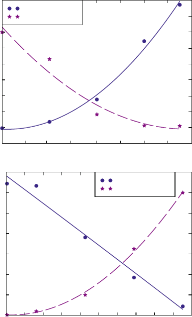
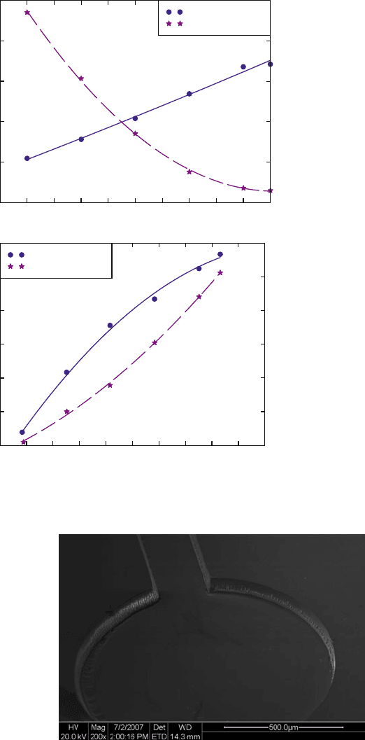
ratio is required to maintain l ow RMS surface roughness. Figure 7.15
shows the dependence of the etch rate and RMS surface roughness as a function
of substrate RF power, chamber pressure, Ar, and SF
6
flow rate. In all cases the
pressure in the chamber was maintained at 0.26 Pa throughout the flow ranges. The
ICP source power was 2000 W and a substrate bias power of 475 W (Bias voltage
of 80 V) was used in generating these results. From the graphs it can be seen that
the best surface roughness of ∼2 nm is obtained at high Ar flow rates, low chamber
pressure, and high substrate power, corresponding to conditions dominated by phys-
ical sputtering of the material. The etch rate can be increased by increasing the SF
6
flow rate from 5 to 50 sccm from 0.54 to 0.74 μm/min, however, the surface rough-
ness was found to degrade under these conditions to >100 nm. Pulse electroplated
nickel was used as the etch mask layer and a selectivity of ∼25:1 was obtained for
SiO
2
etching under these conditions.
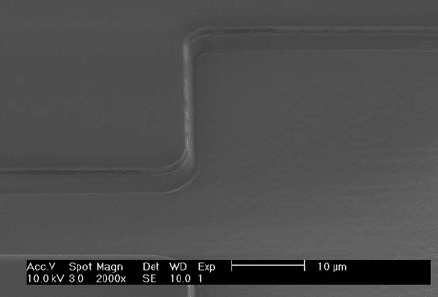
Figure 7.16 shows an SEM of a high-aspect-ratio feature etched in quartz using
these conditions. Similar results were obtained by Li et al. while etching SiO
2
using
Xe instead of Ar. The higher sputter yield of Xe gave a lower RMS surface rough-
ness value as compared to Ar for the same mole fraction of the inert gas in SF
6
.
Although silicone grease or a small drop of Fomblin
R
oil can be used for mounting
the quartz/glass substrates onto a 4 in. silicon carrier wafer, these materials cannot
withstand the long process times and can leave the backside of the sample with
436 S. Tadigadapa and F. Lärmer
hard to remove, stubborn residues. Furthermore, these mounting materials do not
provide a reliable and uniform thermal contact between the carrier wafer and the
sample throughout the entire etch process. In order to avoid these problems, indium
solder can be used for mounting the sample directly onto a silicon wafer. However,
the mounting side of the SiO
2
sample needs to be coated with 20/80 nm of Cr/Au
to provide a surface to which the solder can adhere. Of course if the sample is large
enough it can be directly mechanically clamped or an electrostatic chuck can be
used for the mounting of the sample. In all cases the backside of the chuck/substrate
is cooled using helium gas maintained at the desired temperature.
Pressure (Pa)
Etch Rate (m/min)
rms Surface Roughness (nm)
0.25 0.5 0.75 1 1.25 1.5 1.75 2 2.25 2.5
2.75
0
0.375
80
0.4
160
0.425
240
0.45
320
0.475
400
0.5
480
0.525
560
0.55
Etch Rate
rms Roughness
Substrate Power (W)
Etch Rate (m/min)
rms Surface Roughness (nm)
100 150 200 250 300 350 400 450 500
–20
0.1
0
0.15
20
0.2
40
0.52
60
0.3
80
0.53
100
0.4
210
0.54
140
0.5
160
0.55
Etch Rate
rms Roughness
a
b
Fig. 7.15 Etch rate and surface roughness dependence of Pyrex
R
7740 glass dependence as a
function of: (a) substrate power in watts, (b) chamber pressure in Pa, (c) argon flow rate (sccm),
and (d) SF6 flow rate (sccm). In the above graphs, all other etch parameters except the vari-
able parameter are held constant at the following values: ICP power = 2 kW, substrate power =
475 W, chamber pressure = 0.26 Pa, argon flow rate = 50 sccm, SF6flow rate = 5 sccm, and
substrate temperature − 20
◦
C
7 Dry Etching for Micromachining Applications 437
Argon Flow Rate (sccm)
Etch Rate (m/min)
rms Surface Roughness (nm)
0 5 10 15 20 25 30 35 40 45 50
0
0
6
0.15
12
0.3
18
0.45
24
0.6
30
0.75
Etch rate
rms Roughness
SF
6
Flow Rate (sccm)
Etch Rate (m/min)
rms Surface Roughness (nm)
0 6 12 18 24 30 36 42 48 54 60
0
0.52
20
0.56
40
0.6
60
0.64
80
0.68
100
0.72
1200.76
Etch Rate
rms Roughness
d
c
Fig. 7.15 (continued)
Fig. 7.16 SEM picture of a
60 μm deep etched feature in
quartz. The sidewalls have
been found to be roughened
due to redeposition of
nonvolatile etch products and
mask erosion. Trenching is
also observed at sharp corners
in the feature, clearly
indicating the dominant role
of the ion-induced physical
sputtering in the process [64]
(Used with permission,
copyright 2009, IEEE)
438 S. Tadigadapa and F. Lärmer
7.6.2 High-Aspect-Ratio Etching of Piezoelectric Materials
As seen in the case of SiO
2
, most piezoelectric materials are primarily etched via
physical sputtering with some assistance from chemical species in the process. The
role of the chemical species is clearly observed in the comparative etching exper-
iments of SiO
2
(quartz) and lithium niobate/tantalate [65]. In these experiments it
is clearly observed that increasing the ratio of CF
4
to CHF
3
has no effect on the
etch rate of lithium niobate/tantalate whereas it significantly increased the etch rate
of SiO
2
where a regime of ion-enhanced chemical etching is obtained. Because the
fluorides of lithium and tantalum oxide and niobium oxide are all nonvolatile, the
reactive component of etching is an insignificant part of the etching process, which
simply relies on the physical sputtering of the surface atoms due to the bombard-
ment of energetic ions. Most piezoelectric etching recipes use inert gases as part of
the etch gas composition [66]. This is mainly because inert gases provide plasmas
with higher ion densities and ionization in comparison to the more electronegative
chemical compounds (etch gases) and the higher sputter yield of inert gases is also
much higher than other elements/molecules.
Figure 7.17 shows the SEM of lithium tantalate etched to a depth of ∼8 μmatan
etch rate of 0.2 μm/min. Surface roughness of <5 nm was obtained for this sample.
The etching was performed in an inductively coupled plasma etcher with an SF
6
/Ar
flow rate ratio of 10/50 sccm and a substrate bias voltage of 75 V. The sample surface
roughness is critically dependent on chamber pressure with low pressures offering
a lower RMS surface roughness.
Aluminum nitride is typically etched using chlorine chemistries inasmuch as alu-
minum fluoride is an extremely stable and nonvolatile compound [67, 68]. Shul et al.
have studied the comparative etching of GaN, InN, and AlN in chlorine and BCl
3
plasmas and were able to achieve etch rates of 0.23 μm/min for AlN in BCl
3
plasma
with a small percentage additions of Ar/N
2
[69]. The etching characteristics of ZnO
and etch selectivities of ZnO to SiO
2
in CF
4
/Ar, Cl
2
/Ar, and BCl
3
/Ar plasma are
reported by Woo et al. [70]. High etch rates of 0.12 μm/min have been reported. In
several of the optimization reports of the etch processes, it was important to ensure
that the photoresist mask was able to survive the piezoelectric material patterning.
Fig. 7.17 SEM picture
showing a high aspect ratio,
smooth etching of lithium
tantalate in 10:50 SF
6
:Ar
plasma. The chamber
pressure was <0.66 Pa, with
an ICP power of 2 kW and a
substrate power of 400 W. A
nickel hard mask was used to
pattern the substrate
7 Dry Etching for Micromachining Applications 439
Often such optimization results in a compromise between the etch rate of the
piezoelectric and mask selectivity because such etches are performed under high
pressure and low substrate bias conditions. In cases where it is necessary to use
a hard mask, typically electroplated nickel is used. Nickel provides a very high
selectivity in fluorine plasmas where the selectivities of 20–30:1 for PZT etching
have been reported [71]. PZT is typically etched in fluorine or chlorine plasma.
Using SF
6
and Ar several groups have reported high-aspect-ratio etching of PZT.
Using fluorine-based plasma chemistry, a maximum etch rate of 19 μm/hr for PZT-4
and 25 μm/hr for PZT-5A compositions have been reported [72]. This work also
demonstrated a high-aspect-ratio etch (>5:1) on a 3 μm feature size.
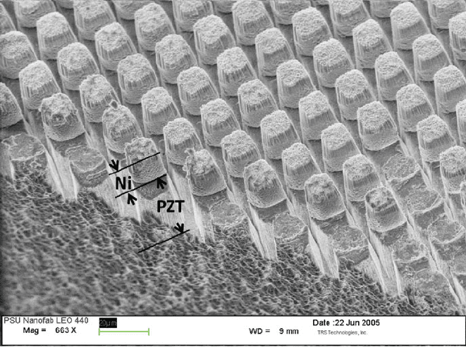
Figure 7.18 shows the SEM image of the etched features for PZT. The square
pillars created have a lateral dimension of 15 μm with a gap of 3 μm in between.
The etched depth was ∼15 μm. Almost vertical sidewalls with relatively smooth
surfaces were obtained. 2–5 μm thick nickel on a Cr/Au was used as the hard
mask. Selectivity of ∼25:1 between the nickel hard mask and PZT was obtained.
The availability of reliable, high-throughput, high-aspect-ratio micromachining pro-
cesses has now created new opportunities for realizing novel MEMS devices from
bulk piezoelectric materials such as quartz, lithium tantalate, aluminum nitride,
PZT, and single-crystal PMN-PT. Table 7.4 summarizes the dry etching of various
piezoelectric materials.
Fig. 7.18 SEM image of the etched feature in PZT ceramic substrate with a minimum feature size
of 3 μm. Almost vertical sidewalls were obtained [73] (Used with permission, copyright 2009,
Institute of Physics)

440 S. Tadigadapa and F. Lärmer
Table 7.4 Summary of the dry etching characteristics of various piezoelectric materials [73]
Material Etch gas(es)
Pressure
(Pa)
RF frequency
(MHz)/power
(W)
Etch rate
(μm/min) Comments
Quartz [74]CF
4
355 27 MHz 4 Nonlithographic plasma
confinement method
was used
Quartz [61]SF
6
/Xe 0.59 13.56/90 0.4 ICP source with 150 W
power was used to
obtain highly smooth
surface
Pyrex 7740/
quartz
[63]
SF
6
/Ar 0.26 13.56/475 0.54 ICP source with 2 kW
power was used. Highly
smooth surface with
R
a
= 1.97 nm. Similar
rates were obtained for
quartz etching as well
LiNbO
3
/
LiTaO
3
[65]
CHF
3
/CF
4
6.58 13.56/350 ∼0.01 Etching proceeds mainly
via physical sputtering
AlN [75]Cl
2
/Ar 0.66 13.56 MHz 0.75 ICP Source with 500 W
power was used.
Etching proceeds by
physical bombardment.
No significant etching
was observed below a
threshold substrate
voltage of −50 V. The
paper also reports
etching GaN and
AlGaN. Another good
reference is [76]
AlN [67] BCl
3
/Cl
2
/Ar 0.66 13.56 MHz 0.4
ZnO [77]SiCl
4
/Ar 23 13.56/0.56 W/m
2
0.027 Additional references on
ZnO etching are
available [70, 78].
Typically etching is
found to proceed via
physical bombardment
ZnO [79]C
2
H
6
/H
2
/Ar 0.66 13.56/300 0.05
PZT (Bulk)
[71]
PZT [80]
PZT [72]
SF
6
CF
4
/80%Ar
SF
6
:Ar::1:10
0.66
1.97
0.66
13.56/200
13.56/700
13.56/475
0.12
0.143
0.42
In [71] pure SF
6
gave the
best etch rate but the
angle was shallow
which could be
improvedbyAr
addition but at the cost
of etch rate. The recipe
used in [72]mainly
uses physical
sputtering, however,
aspect ratios of >5:1
were obtained
Used with permission, copyright 2009, Institute of Physics
7 Dry Etching for Micromachining Applications 441
7.7 Etching of Compound Semiconductors
Almost all III-V compound semiconductors and their heterostructures can be etched
in chlorine and bromine plasmas. More recently CH
4
/H
2
-based dry etching pro-
cesses have also been explored. The three main considerations in the etching of
III-V semiconductor structures include (i) smoothness of etched features inasmuch
as many of these structures are used in optical devices, (ii) low damage to the
semiconductor layer, and (iii) conflicting requirement of high selectivity as well
as equirate etching of the heterostructure layers depending on the particular pro-
cess step. Typically group V halides have very high vapor pressure and therefore
are readily removed in the dry etching process. However, group III halides are not
so volatile. For example, the boiling points of AlCl
3
is 262
◦
C, GaCl
2
is 535
◦
C,
GaCl
3
is 201
◦
C, InCl is 608
◦
C, and InCl
3
∼600
◦
C. Furthermore, group III fluo-
rides are extremely stable compounds and do not volatilize readily; for example, the
boiling point of AlF
3
is 1291
◦
C, GaF
3
is ∼1000
◦
C, and InF
3
is >1200
◦
C. Thus,
purely chemical etching of GaAs can be done in chlorine plasma but the same pro-
cess does not achieve good etching results for InP due to the involatility of InCl
3
.
Furthermore, the addition of fluorine to chlorine plasma can be used to obtain high
selectivity during the etching of GaAs on AlGaAs. Fluorine-containing plasmas also
provide a means for selectively etching silicon nitride and silicon dioxide masks on
III-V compound semiconductors.
The most commonly used masking materials for etching of III–V compounds
include metals such as Cr, Ni, Ti, Al, chemical vapor deposited dielectrics such
as Si
3
N
4
,SiO
2
, and novolac resin-based photoresists and electron beam photore-
sists. Metals exhibit the highest selectivity for these etching applications; however,
the grain size of the deposited film determines the sidewall roughness and lim-
its the achievable smoothness. The smoothest etch results have been achieved
by using hardbaked, multilayer, novolac-resin-based photoresists. In general poly-
methyl methacrylate (PMMA) e-beam resist is found to exhibit poor etch resistance
in comparison to the novolac resists. However, positive tone e-beam resists such as
ZEP-520A and negative tone SAL-601 have been found to offer good etch resis-
tance. Care has to be taken to prevent any erosion of mask which might result in
roughening of the top part of the etched features.
7.7.1 Case Study: Etching of GaAs and AlGaAs
In this section, various GaAs gas chemistries are briefly reviewed. Specific advan-
tages for each process are briefly indicated. Table 7.5 lists the etch rate of some of
the commonly used masking materials in GaAs etching [81].
Reactive Etching in SiCl
4
Plasma: Etching at moderate pressures of 2.63–
13.15 Pa is chemical in nature. Typically at moderate pressure, etching of GaAs
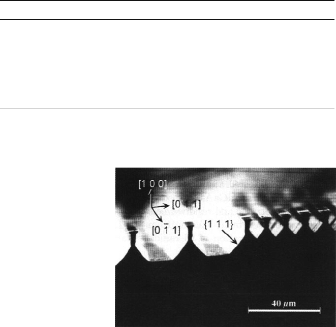
in chlorine and bromine plasma is rapid, spontaneous, and crystallographic as seen
in Fig. 7.19 [37]. The relative chemical etch rates of the various etch planes in GaAs
are: (111)
As - rich
> (100) > (110) > (111)
Ga - Rich
. Silicon tetrachloride is not as
442 S. Tadigadapa and F. Lärmer
Table 7.5 Commonly used masking materials compatible with etching III–V semiconductors in
chlorine plasma
a
Material Etch rate (nm/min) GaAs: material etch rate ratio (selectivity)
GaAs 28.33 1
Au-Pd 2.5 11.3333
Au 1.75 16.19048
Glass (SiO
2
) 0.708333 40
Cr 1.25 22.66667
Ni 0.5 56.66667
Ni-Cr 0.833333 34
AZ-1350 J (Photoresist) 2.916667 9.714286
a
These etch rates were obtained in 90% Ar/10%BCl
3
plasma chemistry obtained in diode RIE
set-up operated at 50 W RF power (300 V bias), 1.97 Pa pressure [81]. Used with permission,
copyright 1987, American Vacuum Society
Fig. 7.19 Etch
characteristics of GaAs in
SiCl
4
reactive ion plasma
(2.63 Pa, 150 W,
200 mW/cm
2
). The high
pressure and low power etch
results in the emergence of
the various crystallographic
facets [37] (Used with
permission, copyright 2000,
Springer)
corrosive as pure Cl
2
gas and the plasma leaves no nonvolatile residues and is a
clean process well suited for crystallographic dry etching.
Reactive Ion Etching in Cl
2
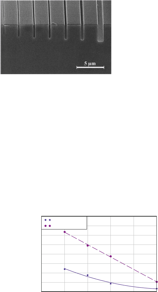
Plasma: Smooth and vertical trenches are obtained
due to the high DC-bias ion bombardment. Aspect-ratio-dependent etch rate is
clearly observed. In order to avoid any roughness or grass formation due to
microloading, this etch must be performed at very low pressures in the range of
0.066–0.66 Pa. The addition of BCl
3
and Ar can result in very smooth trench for-
mation [82]. Figure 7.20 shows an SEM picture of a high-aspect-ratio, smooth etch
profile obtained in GaAs using chlorine plasma [37].
Reactive Ion Etching in BCl
3
+ Ar Plasma: Using this etching chemistry at low
pressures and high Ar%, equirate etching of GaAs and AlGaAs can be obtained. An
equi-etch rate of 280 nm/min for 50 W, 1.97 Pa, and 90% Ar has been reported [81].
Addition of 10% oxygen to this mixture provided a selectivity of ∼5:1, however, at
a remarkably slow etch rate of 10 nm/min for GaAs.
7 Dry Etching for Micromachining Applications 443
Fig. 7.20 Etch characteristics of GaAs in Cl
2
in an inductively coupled plasma reactive ion etcher
(0.2 Pa, 150 W, ∼500 V dc bias). Highly anisotropic etch showing width dependent etch rate is
clearly observed. It is possible to obtain smooth etch morphologies using low pressures (below
0.1 Pa) range [37] (Used with permission, copyright 2000, Springer)
Reactive Ion Etching in SiCl
4
and SiF
4
Plasma: This etch chemistry provides a
high selectivity GaAs etch against AlGaAs. The use of separate chlorine and fluorine
containing gases as opposed to CCl
2
F
2
(CCl
2
F
2
is an ozone depleting chlorofluo-
rocarbon the use of which currently conflicts with “Montreal Protocol”.) affords
greater flexibility in controlling the Cl/F ratio. In addition, no polymer formation is
observed in this gas mixture. Formation of AlF
3
results in the etch stopping mech-
anism for AlGaAs in fluorine containing plasma. Figure 7.21 shows the selectivity
of GaAs over AlGaAs as a function of the percentage of SiCl
4
[83]. Clearly pref-
erential high selectivity of GaAs over AlGaAs is obtained for aluminum-rich GaAs
compositions and at low SiCl
4
concentrations.
Percentage of SiCl
4
Selectivity (Etch Ratio of GaAs: AlGaAs)
0 10 20 30 40 50
0
100
200
300
400
500
600
700
800
Al
0.07
Ga
0.93
As
Al
0.35
Ga
0.65
As
Fig. 7.21 Selectivity of
GaAs over AlGaAs as a
function of %SiCl
4
in
SiCl
4
+ SiF
4
plasma. The
data were obtained for a RIE
plasma at a pressure 7.89 Pa
and a dc bias of −60 V and
offer a selectivity in excess of
500:1 for Al
0.35
Ga
0.65
As [83]
(Used with permission,
copyright 1990, American
Vacuum Society)
Reactive Ion Etching in CH
4
and H
2
Plasma: Hydrogen–alkane mixtures can
also be used to etch GaAs [84, 85]. However, the etch rates in this case are
