Ghodssi R., Lin P., MEMS Materials and Processes Handbook
Подождите немного. Документ загружается.

444 S. Tadigadapa and F. Lärmer
much lower than those achieved using chlorine plasma. In general, hydrogen-based
etches result in very smooth surface morphologies and are not much affected by
water vapor contamination allowing for the use of nonload locked RIE machines.
Furthermore, hydrogen plasma has been demonstrated to result in the least damage
to the substrate [84]. The etching itself is considered to occur through the formation
of AsH
3
and (CH
3
)
3
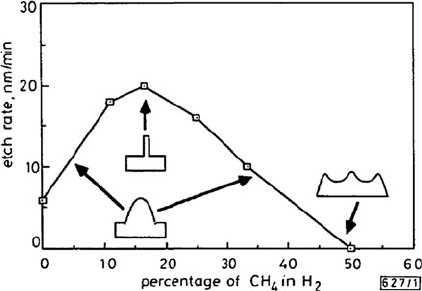
Ga as volatile reaction products. Figure 7.22 shows the depen-
dence of GaAs etch rate as a function of percentage of CH
4
in H
2
plasma [84].
Fig. 7.22 Etch rate of GaAs as a function of %CH
4
in H
2
plasma. The data were obtained for a
RIE plasma at a pressure 1.84 Pa and a power density of 0.4 W/cm
2
. The reduction in the etch rate
with increasing methane is due to the formation of an inert polymer layer. The maximum etch rate
is found to increase to a value of ∼180 nm/min when the etch is performed at a pressure of 5.26 Pa
and 0.75 W/cm
2
[84] (Used with permission, copyright 1987, The Institution of Engineering and
Technology, IET)
7.7.2 Case Study: Etching of InP, InGaAs, InSb, and InAs
Reactive Ion Etching in Cl
2
Plasma: Indium phosphide related materials have
been successfully etched using chlorine plasmas [86–88]. However, owing to the
nonvolatile nature of InCl
3
, etches performed at room temperature including ion
bombardment have been found to exhibit low etch rates and rough morphologies.
Etches performed at elevated temperatures of >140
◦
C show an appreciable increase
in the etch rate of >2 μm/min due to the increased volatilization of InCl
x
.Asthe
temperature is increased to 200–250
◦
C, enhanced energy-driven anisotropy of the
etched features has been observed. However, chemically assisted ion beam etching
performed at high temperatures is prone to microloading-related roughness arising
due to the sputter deposition of nonvolatile residues from hard masks, etch chamber,
and substrate chuck.
Silicon dioxide and photoresist have been found to be suitable etch masks while
graphite and silicon have been found to be suitable for the substrate chuck materi-
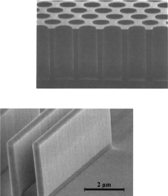
als [89]. Ko et al. have reported the etching of smoothly etched vias in InP using
7 Dry Etching for Micromachining Applications 445
Fig. 7.23 30 μmwide,
92 μm deep via holes etched
in InP using Cl
2
/Ar (50%
Cl
2
) plasma. An ECR source
driven at 500 W along with
100 W RF substrate power at
0.26 Pa and 20
◦
C temperature
was used. Local surface
heating due to ion
bombardment of the substrate
is considered to provide the
elevated temperature [90]
(Used with permission,
copyright 1995, The
Electrochemical Society)
Fig. 7.24 0.4 μm wide slabs etched in InP using Cl
2
/H
2
/N
2
/Ar in an ICP-RIE. A substrate tem-
perature of 250
◦
C, pressure of 0.26 Pa were used [37] (Used with permission, copyright 2000,
Springer)
a ECR-RIE with Cl
2
/Ar as the etch gases (see Fig. 7.23)[90]. A flow ratio of
2:1 of Cl
2
: Ar has been found to result in very smooth etched surface morpholo-
gies. Addition of hydrogen or HCl to the plasma has been shown to improve the
etched surface morphologies. The likely effect of the addition of hydrogen in chlo-
rine plasma is the effective removal of phosphorus as PH
3
. Figure 7.24 shows a very
smooth and vertical etch surface obtained using Cl
2
/H
2
/N
2
/Ar in an ICP-RIE [37].
Etching InP in CH
4
/H
2
Plasma: Alkane–hydrogen etching of InP provides an
alternative to etching using halogen gases. Although the etch rates are low in
the range of 20–60 nm/min, the etch morphologies are extremely smooth and the
damage due to etching is limited to less than 4 nm into the surface [91]. In alkane–
hydrogen plasma, phosphorus is removed via the formation of PH
3
whereas indium
is removed via the formation of (CH
3
)
3
In. Due to the high volatility of PH
3
,the
446 S. Tadigadapa and F. Lärmer
etched surface is found to be In-rich. CH
4
:H
2
ratio in the range of 0.1–0.4 is
typically used. Higher values of CH
4
lead to polymer deposition on the surfaces.
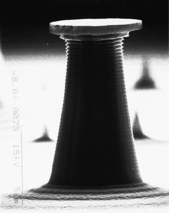
Figure 7.25 shows the etch profile obtained in CH
4
/H
2
/Ar RIE plasma for an
InP/InGaAsP mirror. An overhang and positive etch slope can be seen due to the
buildup of polymer on the sidewall of the etched feature. Cyclically alternating
between O
2
plasma to clear the polymer buildup and etch step using CH
4
/H
2
solves
this problem at the cost of greater process complexity. Alternatively a small amount
of O
2
can be continuously added to the CH
4
/H
2
plasma to prevent the buildup of the
polymer on the sidewalls [92]. A comparison of these methods and their advantages
has been presented by Schramm et al. [93].
Fig. 7.25 A 45 period, gas
source MBE grown
InP/InGaAsP mirror etched
using CH
4
/H
2
/Ar plasma
under conditions: pressure =
6.57 Pa, substrate bias =
500 V, CH
4
/H
2
/Ar : 4/20/10
sccm [93] (Used with
permission, copyright 1997,
The American Vacuum
Society)
7.8 Case Study: Ion Beam Etching
Ion-beam etching is a purely physical, plasma-based etch process and excellent
reviews are available [94, 95]. During milling, the sputtering of material occurs by
momentum transfer between the impinging ions and the surface. To first order, the
etch rate, ER, is proportional to the product of the ion flux density F, and the sputter
yield S(θ), and can be given as [94]
ER(θ, IE) ∝ F cos(θ )S(θ , IE),
where θ is the angle of incidence of the ion beam and IE is the energy of the ion
beam. In general, sputter yield is a function of the angle of incidence, the atomic

7 Dry Etching for Micromachining Applications 447
weight and incident energy of the ions, and the target material. Most materials
exhibit an increase in sputter yield with θ, up to a maximum at about 40
◦
–60
◦
,
followed by a sharp drop. The overall increase in etch rate for oblique angles of
incidence is because the increased sputter yield generally exceeds the reduction in
flux density. The sputter yield also varies with ion energy exhibiting an exponential
increase between 20 and 100 eV, followed by a linear increase up to about 500 eV,
and finally increasing more gradually up to a saturation point above 10 keV [94].
The process is highly anisotropic so undercutting is generally not a concern, and
very high resolutions with features of better than 100 Å have been demonstrated.
The physical nature of the process means that all materials can be etched, allowing
a single-step approach for patterning multimaterial film stacks. However, the major
drawback of ion milling is the poor selectivity, and there is typically less than a
tenfold difference in the etch rate between materials. The etch depth is therefore
controlled by timing, or with mask layer thicknesses adjusted to compensate for
the low selectivity. Table 7.6 lists the etch rates observed in milling experiments
using an Oxford Series-300 dual-source etch system with a 15 cm Kaufman-type
ion source. All tests were performed using argon at a pressure of 0.026–0.039 Pa.
The use of oblique angle increases the etch rate as well as avoids trenching and
redeposition problems.
Table 7.6 Ion-beam etch rates for some commonly ion-milled materials
a
Material Current density (mA/cm
2
) Voltage (V) Angle (
◦
) Etch rate (nm/min)
PZT 0.42 1000 0 14
PZT 0.45 1000 45 24
Platinum 0.42 1000 0 30
Platinum 0.45 1000 45 34
Si
x
N
y
0.45 1000 45 28
Zirconia 0.45 1000 45 20
a
Milling conditions: 0.026–0.039 Pa [26]
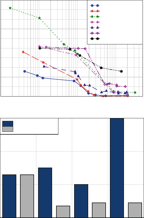
The addition of a partial pressure of oxygen during ion-beam etching has been
noticed to reduce the sputter yield of certain metals that oxidize easily [96].
Figure 7.26a shows the etch rate as a function of oxygen concentration for various
materials. The effect is likely the result of competition at the surface between the
chemisorption of oxygen, and the sputtering removal of both the oxygen and metal
atoms. This method can be used as a means to increase the selectivity of a mask
over nonreactive materials. This is well illustrated for patterning complex oxides
such as lead zirconate titanate (PZT), where reactive sputtering in oxygen ambient
has little effect on its milling rate, however, the ion milling etch rates of metals
such as chrome, titanium, and aluminum are significantly reduced due to harder to
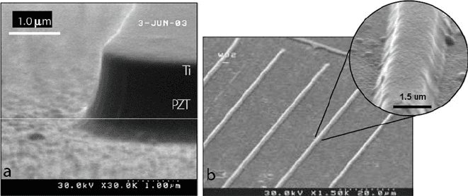
etch metal–oxide formation (see Fig. 7.26b). Figure 7.27a shows PZT etching with
nearly vertical sidewalls achieved using a titanium mask layer. Using this technique
it is possible to pattern thin PZT features down to ∼1 μm as shown in Fig. 7.27b.
448 S. Tadigadapa and F. Lärmer
Oxygen Partial Pressure (x10
–3
Pa)
Etching Rate (nm/min)
1 2 3 4 5 7 10 20 30 50 100 200 500 1000 2000 5000
0
5
10
15
20
25
30
35
40
45
50
Vanadium
Chromium
Bulk Aluminum
Aluminum (Film)
Manganese
Silicon
Silicon Dioxide
Etch Rate (nm/min)
0
20
40
60
PZT Chromium Titanium Aluminum
0.53 Pa, Ar Only
0.53 Pa, 2:1::O
2
:Ar
a
b
Fig. 7.26 (a) Etch rate of various materials with the addition of oxygen at 1 keV and 0.6 mA/cm
2
current density [ 96] (Used with permission, copyright 1973, Springer); (b) ion milling rates for
sputtered metals and sol-gel deposited PZT with and with without oxygen using 0.45 mA/cm
2
current density, 1 kV acceleration potential, angle of 45
◦
and a pressure of 0.53 Pa
7 Dry Etching for Micromachining Applications 449
Fig. 7.27 Ion-beam etching PZT with hard masks in O
2
, showing excellent resolution: (a)PZT
patterned using titanium hard mask, and (b) using chromium hard mask [26]
7.9 Summary
To summarize, dry etching processes are at the heart of MEMS fabrication and mate-
rials technology. The use of plasma creates a reactive gaseous environment in which
various substrate materials can be removed as volatile reaction products. Most of the
etching processes are based on various halogen chemistries. The overall etch results
depend upon the specific material, etch chemistry, etch equipment, and various other
parameters including masking materials, history of the chamber, and so on, thus it
is nearly impossible to give specific process recipes that can be reliably reproduced
across various laboratories or facilities. What is important is to realize the deter-
mining factors of the overall etch characteristics in a given process. In Table 7.7,
process recipes for etching various metals, semiconductors, and dielectrics are
listed. These are not intended as a list of the current state-of-the-art numbers,
but to provide the reader with nominal etch-related parameters to be expected
on three different but typical pieces of etch equipment. Recent developments in
high vacuum technology with high-throughput turbomolecular pumps, high-density
and stable inductively coupled plasma sources, fast switching, precision mass flow
controllers, and process control instrumentation have enabled the design and man-
ufacturing of next-generation etching equipment. However, challenges remain in
the development of high-throughput, high-definition etching processes, especially
for high-aspect-ratio etching of ceramic materials such as complex oxides encoun-
tered in piezoelectric and magnetic materials, and wideband gap semiconductors.
In addition, challenges lie ahead as top-down fabrication techniques are rapidly
approaching the 10 nm scale with high-aspect-ratio etch requirements.

450 S. Tadigadapa and F. Lärmer
Table 7.7 Typical plasma etch recipes including gas chemistry used, etch rates obtained, and equipment type
Material
Pressure
(Pa)
Source power
(W)
Substrate
power (W) Gases
Etch rate
(nm/min) Comments
Metals
Aluminum 1.32 800 175 Cl
2
: 75 100 Tool: Applied Materials DPS System, Mask:
PR 3012
Platinum 1.32 800 175 Cl
2
: 75 sccm 100 Tool: Applied Materials DPS System, Mask:
PR 3012
Chromium 10.5 75 − Cl
2
: 60 sccm,
O
2
: 20 sccm
10 Tool: Plasma Therm PT 720 Mask: ZEP-530
(Selectivity: PR:Cr::3:2) Note: 60% over
etch recommended for small features (sub
750 nm)
Semiconductors
Silicon 1.32 1000 150 Cl
2
: 20 sccm 490−520 Tool: Applied Materials DPS System, Mask:
SiO
2
Selectivity: Si:SiO
2
::8:1
Silicon 1.32 175 − Cl
2
: 20 sccm 60 Tool: Plasma Therm PT 720, Mask: Cr,
Selectivity: Si:Cr :: 10:1. Process relies on
oxidation of chromium for good selectivity
Silicon 26.3 200 − SF
6
: 50 sccm 300−400 Tool: Plasma Therm PT 720, Mask: SiO
2
,
Selectivity: Si:SiO
2
:: 60:1
Gallium arsenide 0.132 200 − Cl
2
: 20 sccm 500 Tool: Plasma Therm PT 720, Mask: PR,
Selectivity: GaAs:PR :: 20:1, Mask: Cr,
Selectivity: GaAs:Cr :: 50:1
AlGaAs 1.32 250 − Cl
2
: 29 sccm 400 Tool: Plasma Therm PT 720, Mask: PR,
Selectivity: AlGaAs:PR :: > 10:1

7 Dry Etching for Micromachining Applications 451
Table 7.7 (continued)
Material
Pressure
(Pa)
Source power
(W)
Substrate
power (W) Gases
Etch rate
(nm/min) Comments
Dielectrics
Silicon dioxide 1.97 − 100 CHF
3
: 75 sccm
CF
4
: 30 sccm
37−40 Tool: Applied Materials MERIE System,
Magnetic Field: 60 gauss
Silicon dioxide 13.2 200 − CF
4
: 45 sccm
O
2
: 5 sccm
110 Tool: Plasma Therm PT 720 Mask: PR 1813
Silicon nitride 1.97 − 50 CHF
3
: 25 sccm 10 Tool: Applied Materials MERIE System,
Magnetic Field: 60 gauss
Silicon Nitride 26.3 300 − CF
4
: 40 sccm
O
2
: 8 sccm
Ar: 7 sccm
167 Tool: Plasma Therm PT 720 Mask: PR 1813,
Selectivity: < 1
Quartz 6.57 − 200 CHF
3
: 45 sccm
Ar: 140 sccm
46−49 Tool: Applied Materials MERIE System,
Magnetic Field: 22.5 gauss, Mask:
Chromium, Selectivity: Quartz:Cr :: 12:1
SilSpin
R
2.63 − 25 O
2
: 30 sccm
CHF
3
: 12 sccm
130 Tool: Applied Materials MERIE System,
Magnetic Field: 45 gauss, Cathode
temperature: 3
◦
C
Polyimide 2.37 − 150 O
2
: 90 sccm 682 Tool: Applied Materials MERIE System,
Magnetic field: 45 gauss, Cathode
temperature: 3
◦
C,Mask:CrorNiHard
Mask
Polypyrrole 5.26 350 − O
2
: 30 sccm 300 Tool: Plasma Therm PT 720 Mask: PR 1813,
Selectivity: Polypyrrole:PR ::1:1
Benzocyclobutene (BCB) 26.3 200 − O
2
: 45 sccm
Ar: 5 sccm
CF
4
: 10 sccm
1000 Tool: Plasma Therm PT 720, Process used for
BCB etch back
Source: The Pennsylvania State University node of the National Nanofabrication Infrastructure Network
Note: The PlasmaTherm PT-720 is a parallel plate etcher (i.e., diode type etcher), AMAT-MERIE is a magnetically enhanced reactive ion etcher and uses
a magnetic field for increasing the plasma density, and AMAT-DPS is a high-density inductively coupled plasma etcher in which the plasma power and
substrate power are independently controlled
452 S. Tadigadapa and F. Lärmer
Acknowledgment The author (ST) would like to thank the graduate students Steven Gross, Han
Guen Yu, Abhijat Goyal, Saliya Subasinghe, and Ping Kao in the group and Guy Lavallee and
Changjun Huang at the Pennsylvania State University (PSU) Nanofabrication facility. ST acknowl-
edges the use of facilities at the PSU Site of the NSF NNIN under Agreement 0335765. ST also
acknowledges financial support from the US Army Research Office (Grant # W911NF-07-1-0327)
and NSF (Grant # 0925438).
References
1. R.J. Shuhl, S.J. Pearton: Handbook of Advanced Plasma Processing Techniques, p. 653
(Springer, Heidelberg, 2000)
2. S.M. Rossnagel, W.D. Westwood, J.J. Haber: Handbook of Plasma Processing Technology:
Fundamental, Etching, Deposition and Surface Interactions, p. 546 (William Andrew,
New York, NY, 1991)
3. D.M. Manos, D.L. Flamm: Plasma Etching: An Introduction, p. 476 (Academic, San Diego,
CA, 1989)
4. M. Elwenspoek, H.V. Jansen: Silicon Micromachining (Cambridge University Press,
Cambridge, 1998)
5. M. Madou: Fundamentals of Mirofabrication (CRC Press, Boca Raton, FL, 1997)
6. G.S. Oehrlein, W.D. Westwood, J.J. Haber: Reactive Ion Etching, in Reactive Ion Etching:
Handbook of Plasma Processing Technology, pp. 196–206 (Rossnagel, S.M. (Ed.) Noyes,
New York, NY, 1990)
7. G.C. Schwartz, P.M. Schaible: Reactive ion etching of silicon, J. Vac. Sci. Technol. 16, 410–
413 (1979)
8. X.Y. Li, P.J. French, P.M. Sarro, R.F. Wolffenbuttel: Fabrication of a Single Crystalline
Silicon Capacitive Lateral Accelerometer Using Micromachining Based on Single Step
Plasma Etching. Proceedings of the IEEE MEMS Conference, Amsterdam, The Netherlands,
pp. 398–403, 1995.
9. B. Diem, P. Rey, S. Renard, S.V. Bosson, H. Bono, F. Michel, M.T. Delaye, G. Delapierre: SOI
’SIMOX’; from bulk to surface micromachining, a new age for silicon sensors and actuators,
Sens. Actuators A Phys. 46, 8–16 (1995)
10. K.T. Sung, S.W. Pang: Etching of Si with Cl
2
using an electron cyclotron resonance source.
39th National Symposium of the American Vacuum Society, Chicago, IL, pp. 1206–1210
(1993)
11. W.H. Juan, J.W. Weigold, S.W. Pang: Dry etching and boron diffusion of heavily doped high-
aspect ratio Si trenches. Micromachining and Microfabrication Process Technology II, Austin,
TX, pp. 45–55 (1996)
12. C.J. Mogab: The loading effect in plasma etching, J. Electrochem. Soc. 124, 1262–1268
(1977)
13. D.L. Flamm: Introduction to Plasma Chemistry, in Plasma Etching: An Introduction, pp. 91–
183 (Manos, D.M., Flamm, D.L. (Eds.) Academic, San Diego, CA, 1989)
14. G.S. Hwang, K.P. Giapis: On the origin of the notching effect during etching in uniform high
density plasmas, J. Vac. Sci. Technol. B Microelectron, Nanometer Struct. 15, 70–87 (1997)
15. K.P. Giapis: Fundamentals of Plasma Process-Induced Charging and Damage, in Handbook
of Advanced Plasma Processing Techniques, pp. 257–308 (Shuhl, R.J., Pearton, S.J. (Eds.)
Springer, Berlin, 2000)
16. B. Chapman: Glow Discharge Processes: Sputtering and Plasma Etching (Wiley-Interscience,
New York, NY, 1980)
17. M. de Boer, H. Jansen, M. Elwenspoek: The Black Silicon Method V: A Study of The
Fabricating of Movable Structures for Micro Electromechanical Systems in Solid-State
Sensors and Actuators, 1995 and Eurosensors IX. Transducers 95. The 8th International
Conference, pp. 565–568 (1995).
7 Dry Etching for Micromachining Applications 453
18. H. Muenzel, G. Benz, A. Schilp, F. Laermer: Processing silicon in a plasma etch system
(fabrication of free-standing silicon structures) Patent DE4420962, GB2,290,413, Office, G.P.,
Germany (1995)
19. K.A. Shaw, Z.L. Zhang, N.C. MacDonald: SCREAM I: A single mask, single-crystal silicon,
reactive ion etching process for microelectromechanical structures, Sens. Actuators A Phys.
40, 63–70 (1994)
20. D.E. Ibbotson, J.A. Mucha, D.L. Flamm, J.M. Cook: Plasmaless dry etching of silicon with
fluorine-containing compounds, J. Appl. Phys. 56, 2939–2942 (1984)
21. F.I. Chang, R. Yeh, G. Lin, P.B. Chu, E. Hoffman, E.J.J. Kruglick, K.S.J. Fister, M.H. Hecht:
Gas-Phase Silicon Micromachining with Xenon Difluoride. Proceedings of the SPIE, Austin,
TX, 1995, Vol. 2641, pp. 117–128 (1995).
22. X.-Q. Wang, X. Yang, K. Walsh, Y.-C. Tai: Gas-Phase Silicon Etching with Bromine
Trifluoride. Proceedings of the International Conference on Solid-State Sensors and
Actuators - Transducers 97, Chicago, Vol. 2, p. 1505 (1997).
23. Y. Saito, O. Yamaoka, A. Yoshida: Plasmaless etching of silicon using chlorine trifluoride,
J. Vac. Sci. Technol. B: Microelectron. Nanometer Struct. 9, 2503–2506 (1991)
24. G.T.A. Kovacs, N.I. Maluf, K.E. Petersen: Bulk micromachining of silicon, Proc. IEEE 86,
1536–1551 (1998)
25. K.R. Williams, R.S. Muller: Etch rates for micromachining processing, J. Microelectromech.
Syst. 5, 256–269 (1996)
26. S.J. Gross: Micromachined switches and cantilever actuators based on piezoelectric lead
zirconate titanate (PZT), Ph.D. Thesis, Electrical Engineering, The Pennsylvania State
University, University Park, pp. 66–70 (2004).
27. C. Leinenbach, H. Seidel, T. Fuchs, S. Kronmueller, F. Laermer: A novel sacrificial layer
technology based on highly selective etching of silicon-germanium in CLF
3
in Micro Electro
Mechanical Systems, 2007. MEMS IEEE 20th International Conference, pp. 65–68 (2007).
28. A. Hoechst: Plasmaless Dry Etching of Silicon Using Chlorine Trifluoride. Investigation of
Etching Mechanism and Applications in Microsystem Technologies, Ph.D. Thesis, pages 118,
University of Tubingen, Germany, (2007).
29. A. Hoechst, F. Fischer, G. Kirbach, A. Urban, V. Becker, M. Irmscher, H. Sailer, D.P. Kern:
Investigations on the mechanism of silicon etching with chlorine-trifluoride, J. Vac. Sci.
Technol. B: Microelectron. Nanometer Struct. 23, 1936–1942 (2005)
30. O.A. Popov: High Density Plasma Sources (Noyce Publications, Park Ridge, NJ, 1995)
31. D.L. Flamm, K.G. Herb: Plasma Etching Technology – An Overview, in Plasma Etching: An
Introduction, pp. 1–89 (Manos, D.M., Flamm, D.L. (Eds.) Academic, San Diego, CA, 1989)
32. F. Laermer, A. Schilp, K. Funk, M. Offenberg: Bosch deep silicon etching: improving unifor-
mity and etch rate for advanced MEMS applications in Micro Electro Mechanical Systems,
1999. MEMS99. 12th IEEE International Conference, pp. 211–216 (1999)
33. V. Becker, F. Laermer, A. Schilp, T. Beck: Plasma Etching Installation Patent 6,531,031,
Office, U.S.P., US (2003)
34. K. Breitschwerdt, V. Becker, F. Laermer, A. Schilp: Device and Method for Etching a
Substrate by using an Inductively Coupled Plasma Patent 6,709,546 and 7,094,706, Office,
U.S.P., US (2004)
35. B. Charlet, L. Peccoud: Process for Etching with Gaseous Plasma, Patent EP-0359777, Office,
E.P., France (1992)
36. B. Charlet, L. Peccoud, T. Dupeux: Microusinage du silicium dans un reacteur GIR assiste
par un plasma micro-ondes. Proceedings 6th Colloque Int. sur la Pulverisation Cathodique et
ses Applications, CIP 85, Nice, France, pp. 183–188 (1987).
37. C. Youtsey, I. Adesida: Plasma Processing of III-V Materials, In Handbook of Advanced
Plasma Processing Techniques, pp. 459–506 (Shuhl, R.J., Pearton, S.J. (Eds.) Springer, Berlin,
2000)
38. J.W. Coburn, H.F. Winters: Ion- and electron-assisted gas-surface chemistry – An important
effect in plasma etching, J. Appl. Phys. 50, 3189–3196 (1979)
