Fitzgerald A.E. Electric Machinery
Подождите немного. Документ загружается.

516 CHAPTER 10 Introduction to Power Electronics
inductive, a positive load current will be flowing at this time, and that load current
will immediately transfer to the short circuit corresponding to diode D2. At the same
time, the current through diode D 1 will immediately drop to zero, diode D 1 will be
reverse biased by the source voltage, and it will turn OFF. This operating condition is
shown in Fig. 10.21 c. Thus, the diodes in this circuit alternately switch ON and OFF
each half cycle: D1 is ON when Vs(t) is positive, and D2 is ON when it is negative.
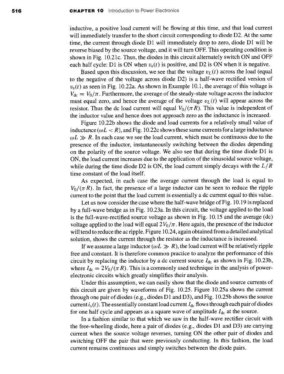
Based upon this discussion, we see that the voltage
VL (t)
across the load (equal
to the negative of the voltage across diode D2) is a half-wave rectified version of
Vs(t) as seen in Fig. 10.22a. As shown in Example 10.1, the average of this voltage is
Vdc =
Vo/rr.
Furthermore, the average of the steady-state voltage across the inductor
must equal zero, and hence the average of the voltage
VL (t)
will appear across the
resistor. Thus the dc load current will equal
Vo/(rc R).
This value is independent of
the inductor value and hence does not approach zero as the inductance is increased.
Figure 10.22b shows the diode and load currents for a relatively small value of
inductance
(coL < R),
and Fig. 10.22c shows these same currents for a large inductance
coL
>> R. In each case we see the load current, which must be continuous due to the
presence of the inductor, instantaneously switching between the diodes depending
on the polarity of the source voltage. We also see that during the time diode D 1 is
ON, the load current increases due to the application of the sinusoidal source voltage,
while during the time diode D2 is ON, the load current simply decays with the L/R
time constant of the load itself.
As expected, in each case the average current through the load is equal to
Vo/(Jr R).
In fact, the presence of a large inductor can be seen to reduce the tipple
current to the point that the load current is essentially a dc current equal to this value.
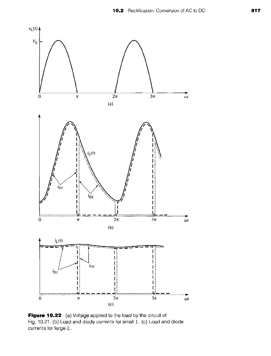
Let us now consider the case where the half-wave bridge of Fig. 10.19 is replaced
by a full-wave bridge as in Fig. 10.23a. In this circuit, the voltage applied to the load
is the full-wave-rectified source voltage as shown in Fig. 10.15 and the average (dc)
voltage applied to the load will equal 2
Vo/zr.
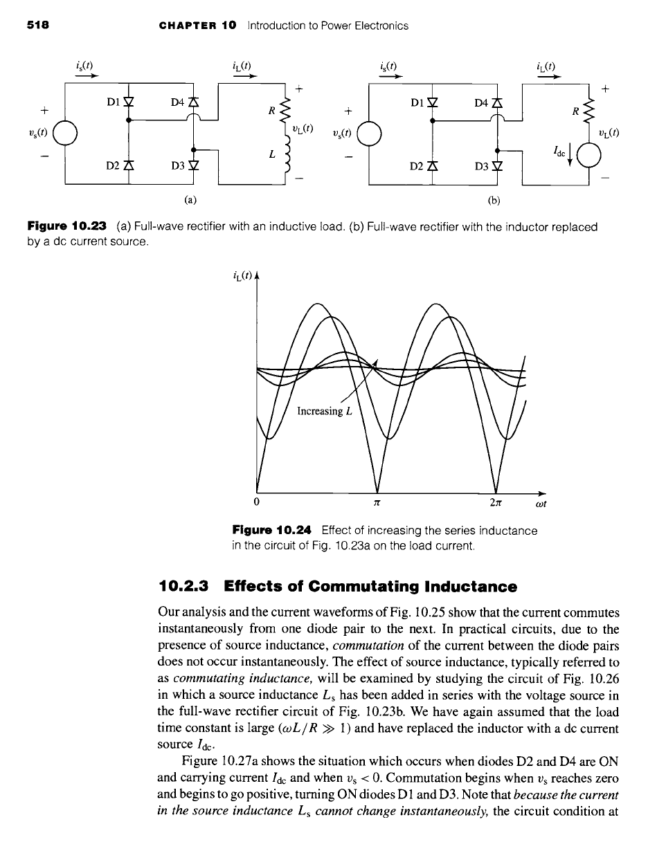
Here again, the presence of the inductor
will tend to reduce the ac ripple. Figure 10.24, again obtained from a detailed analytical
solution, shows the current through the resistor as the inductance is increased.
If we assume a large inductor
(wL
>> R), the load current will be relatively ripple
free and constant. It is therefore common practice to analyze the performance of this
circuit by replacing the inductor by a dc current source lac as shown in Fig. 10.23b,
where lac = 2 V0/(zr R). This is a commonly used technique in the analysis of power-
electronic circuits which greatly simplifies their analysis.
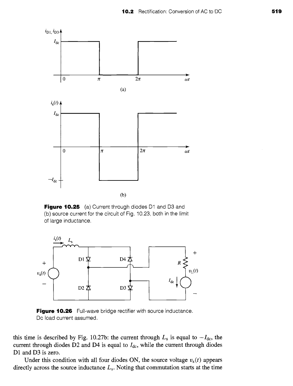
Under this assumption, we can easily show that the diode and source currents of
this circuit are given by waveforms of Fig. 10.25. Figure 10.25a shows the current
through one pair of diodes (e.g., diodes D1 and D3), and Fig. 10.25b shows the source
current i~ (t). The essentially constant load current lac flows through each pair of diodes
for one half cycle and appears as a square wave of amplitude l, jc at the source.
In a fashion similar to that which we saw in the half-wave rectifier circuit with
the free-wheeling diode, here a pair of diodes (e.g., diodes D 1 and D3) are carrying
current when the source voltage reverses, turning ON the other pair of diodes and
switching OFF the pair that were previously conducting. In this fashion, the load
current remains continuous and simply switches between the diode pairs.
o
c-
.-i
.-i
(1)
.-i.,
0
m
77"11
o~
k~
• .o
0
~o <
0_ ~ :M
~o
o~
3
0 (I)
v
r_ o
c-~ c_
0
0_
0
O_
(1)
c:r
L-
t-
r
518 CHAPTER 10 Introduction to Power Electronics
is(t)
/
+ D1 ~ D4
Vs(t)
D2 D3
iL(t) is(t)
+
R
VL(t)
L
+
Vs(t) (
I
D1 @ D4
D2 D3
(a) (b)
iL(t)
R +
Idc~ ~(t)
Figure
10,23 (a) Full-wave rectifier with an inductive load. (b) Full-wave rectifier with the inductor replaced
by a dc current source.
iL(t)
easln
,,,.-
0 ~: 2Jr wt
Figure
10.24 Effect of increasing the series inductance
in the circuit of Fig. 10.23a on the load current.
10.2.3 Effects of Commutating Inductance
Our analysis and the current waveforms of Fig. 10.25 show that the current commutes
instantaneously from one diode pair to the next. In practical circuits, due to the
presence of source inductance, commutation of the current between the diode pairs
does not occur instantaneously. The effect of source inductance, typically referred to
as commutating inductance, will be examined by studying the circuit of Fig. 10.26
in which a source inductance Ls has been added in series with the voltage source in
the full-wave rectifier circuit of Fig. 10.23b. We have again assumed that the load
time constant is large (coL/R >> 1) and have replaced the inductor with a dc current
source Idc.
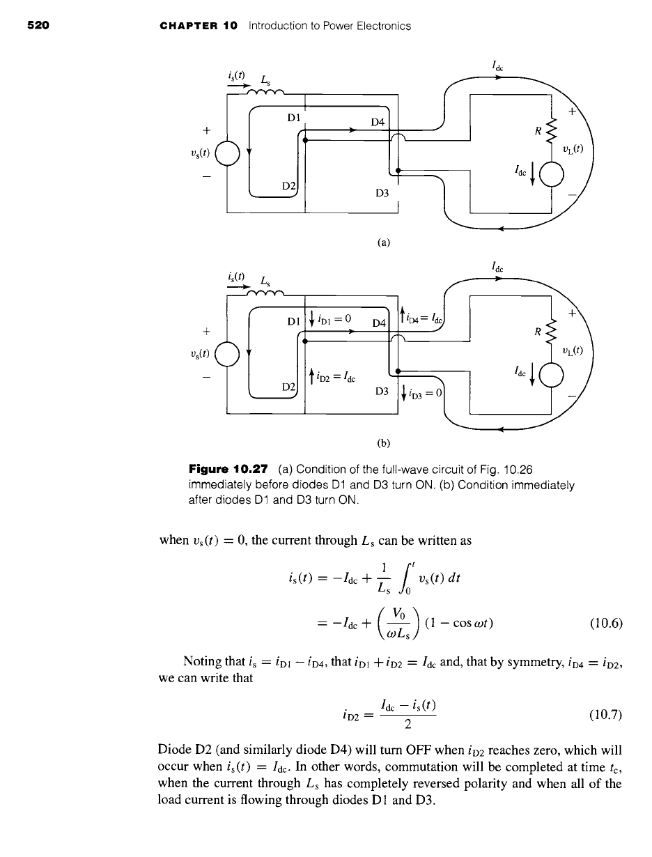
Figure 10.27a shows the situation which occurs when diodes D2 and D4 are ON
and carrying current 10c and when Vs < 0. Commutation begins when Vs reaches zero
and begins to go positive, turning ON diodes D 1 and D3. Note that because the current
in the source inductance Ls cannot change instantaneously, the circuit condition at
10.2 Rectification: Conversion of AC to DC 519
iD1, iD3
Idc
is(t)
I~c
--Idc -
27r
wt
(a)
>
2re wt
(b)
Figure 10.25 (a)
Current through diodes D1 and D3
and
(b)
source current
for the circuit of Fig. 10.23, both in
the limit
of
large inductance.
is(t)
L s
r
+ DI@
Vs(t)
D2
D4 2
f
D3 ~.
R +
/dc ~ (t)
Figure 10.26 Full-wave bridge rectifier with source inductance.
Dc
load current assumed.
this time is described by Fig. 10.27b: the current through Ls is equal to --Idc, the
current through diodes D2 and D4 is equal to/de, while the current through diodes
D 1 and D3 is zero.
Under this condition with all four diodes ON, the source voltage Vs(t) appears
directly across the source inductance Ls. Noting that commutation starts at the time
520 CHAPTER 10 Introduction to Power Electronics
+
Vs(t) Q
-[
is(t) L s
I
D1
D
de
• D4 j
I
(a)
is(t) L s
D
+
Vs(t) Q
~iDl --0
f iD2 = Idc
c
D iD4= ld~c R
(b)
Figure
10.27 (a) Condition of the full-wave circuit of Fig. 10.26
immediately before diodes D1 and D3 turn ON. (b) Condition immediately
after diodes D1 and D3 turn ON.
when Vs(t) - 0, the current through Ls can be written as
1/o'
is(t) -- --Idc + -~s Vs(t) dt
-- -/de + ~s (1 -- COS
wt)
(10.6)
Noting that is -- iDI --
iD4,
that iD1 + iD2 = Idc and, that by symmetry, iD4 =- iD2,
we can write that
Idc - is(t)
iD2 = (10.7)
2
Diode D2 (and similarly diode D4) will turn OFF when iD2 reaches zero, which will
occur when is(t) - Idc. In other words, commutation will be completed at time tc,
when the current through Ls has completely reversed polarity and when all of the
load current is flowing through diodes D 1 and D3.
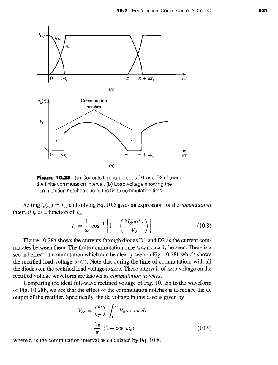
10.2 Rectification Conversion of AC to DC 521
IDC"
D1
0 COt c
n + cot~
).
cot
(a)
VL(t)
v0
Commutation
notches
cot c Jr Jr + cot c
r
cot
(b)
Figure
10.28 (a) Currents through diodes D1 and D2 showing
the finite commutation interval. (b) Load voltage showing the
commutation notches due to the finite commutation time.
Setting is(tc) = Idc and solving Eq. 10.6 gives an expression for the
commutation
interval tc
as a function of Idc
1 , [ ( ,dc Ls)l
tc=-- cos 1- ~ (10.8)
oJ V0
Figure 10.28a shows the currents through diodes D 1 and D2 as the current com-
mutates between them. The finite commutation time tc can clearly be seen. There is a
second effect of commutation which can be clearly seen in Fig. 10.28b which shows
the rectified load voltage
VL (t).
Note that during the time of commutation, with all
the diodes on, the rectified load voltage is zero. These intervals of zero voltage on the
rectified voltage waveform are known as
commutation notches.
Comparing the ideal full-wave rectified voltage of Fig. 10.15b to the waveform
of Fig. 10.28b, we see that the effect of the commutation notches is to reduce the dc
output of the rectifier. Specifically, the dc voltage in this case is given by
( i~V°sinc°tdt
Vdc- \~-/
v0
= (1 + cos Wtc) (10.9)
Jr
where tc is the commutation interval as calculated by Eq. 10.8.
522 CHAPTER
10 Introduction to Power Electronics
Finally, the dc load current can be calculated as function of tc
Vac V0
/ac = = (1 + coscotc) (10.10)
R arR
Substituting Eq. 10.8 into Eq. 10.10 gives a closed-form solution for lac
2Vo
/~c = (10.11)
rrR + 2coL~
and hence
2V0
Vdc =/acR = (10.12)
2ogLs
2"/'+ R
We have seen that commutating inductance (which is to a great extent unavoidable
in practical circuits) gives rise to a finite commutation time and produces commutation
notches in the rectified-voltage waveform which reduces the dc voltage applied to
the load.
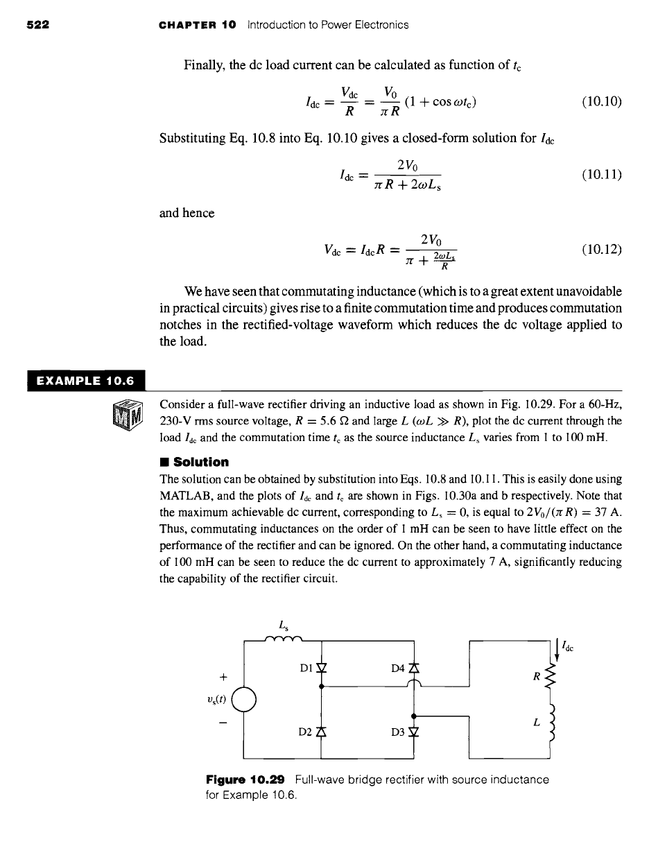
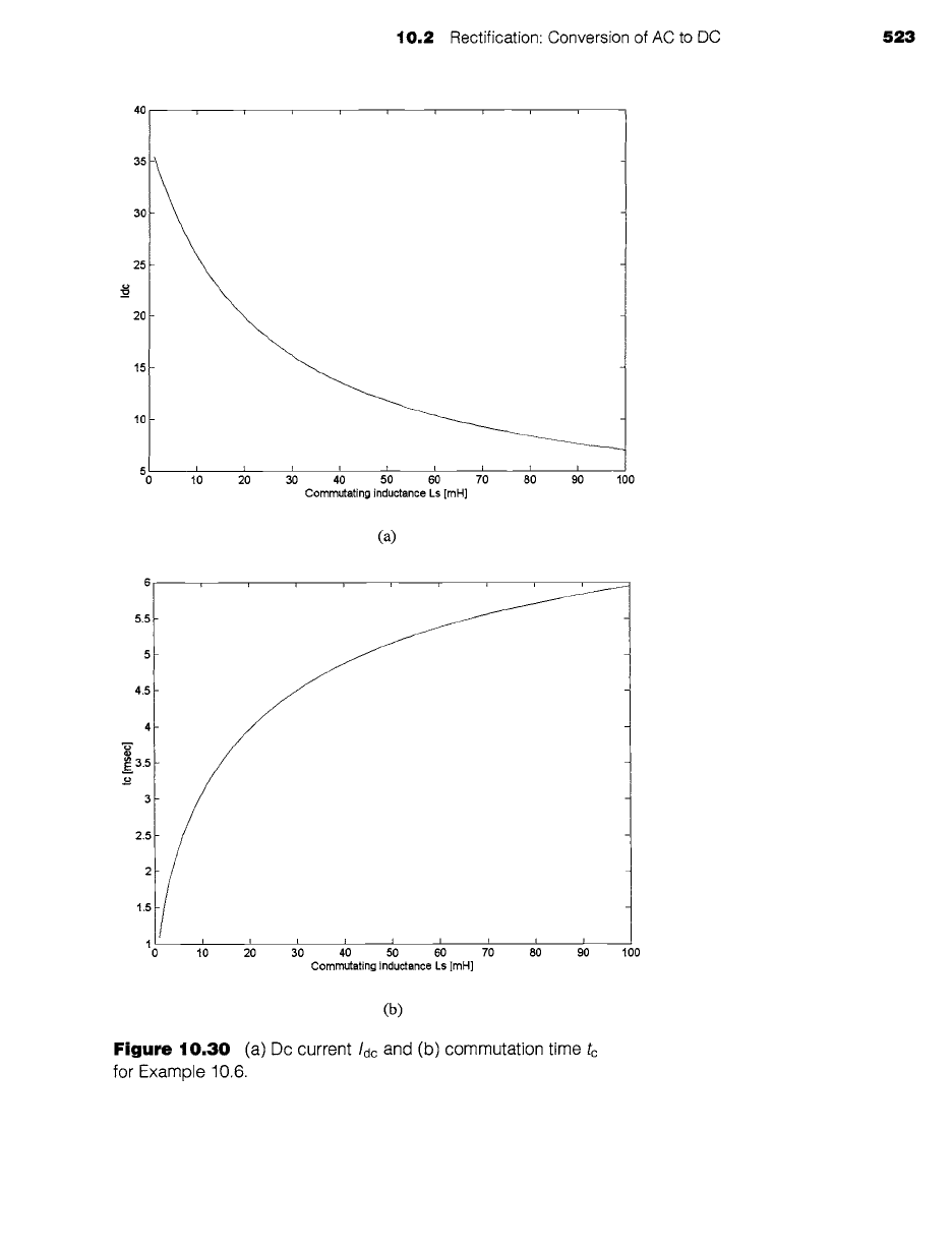
EXAMPLE 10.6
Consider a full-wave rectifier driving an inductive load as shown in Fig. 10.29. For a 60-Hz,
230-V rms source voltage, R = 5.6 f2 and large L (coL >> R), plot the dc current through the
load Idc and the commutation time tc as the source inductance L~ varies from 1 to 100 mH.
m Solution
The solution can be obtained by substitution into Eqs. 10.8 and 10.11. This is easily done using
MATLAB, and the plots of Idc and tc are shown in Figs. 10.30a and b respectively. Note that
the maximum achievable dc current, corresponding to L, = 0, is equal to 2V0/(rr R) = 37 A.
Thus, commutating inductances on the order of 1 mH can be seen to have little effect on the
performance of the rectifier and can be ignored. On the other hand, a commutating inductance
of 100 mH can be seen to reduce the dc current to approximately 7 A, significantly reducing
the capability of the rectifier circuit.
+
°s(t) (
m
)
t s
D1
D2
~_Z D4
2
(
x D3
~.
c
R
L
Figure 10.29
Full-wave bridge rectifier with source inductance
for Example 10.6.
40 , , , , i
35
30
25
o
2O
10-
5.5
10.2 Rectification: Conversion of AC to DC 523
~o ;o ~'o ~'o io ~'o ~'o ;o ~'o
Commutating inductance Ls [mH]
9=0 1
O0
Ca)
4.5
/
4
E
3.5
3
2.5
2
1.5
~o ;o do ~'o io ~'o ~'o ;o ~'o ~'o
Commutating inductance Ls [mH]
100
(b)
Figure 10.30 (a) Dc current /dc and (b) commutation time to
for
Example 10.6.

524 CHAPTER 10 Introduction to Power Electronics
Here is the MATLAB script for Example 10.6.
clc
clear
%parameters
omega : 2"pi'60;
R : 5.6;
V0 : 230*sqrt(2) ;
for n = i:i00
Ls(n) = n*le-3;
Idc(n) = 2*V0/ (pi*R + 2*omega*Ls(n) ) ;
tc(n) = (i/omega)*acos(l-(2*Idc(n)*omega*Ls(n))/V0) ;
end
plot (Ls*1000, Idc)
xlabel('Commutating inductance Ls [mH] ')
ylabel ( ' Idc' )
fprintf('\nHit any key to continue\n')
pause
plot (Ls*1000, tc*1000)
xlabel('Commutating inductance Ls [mH] ')
ylabel('tc [msec] ')
Calculate the commutating inductance and the corresponding commutation time for the circuit
of Example 10.6 if the dc load current is observed to be 29.7 A.
Solution
L~ = 5.7 mH and tc = 2.4 msec
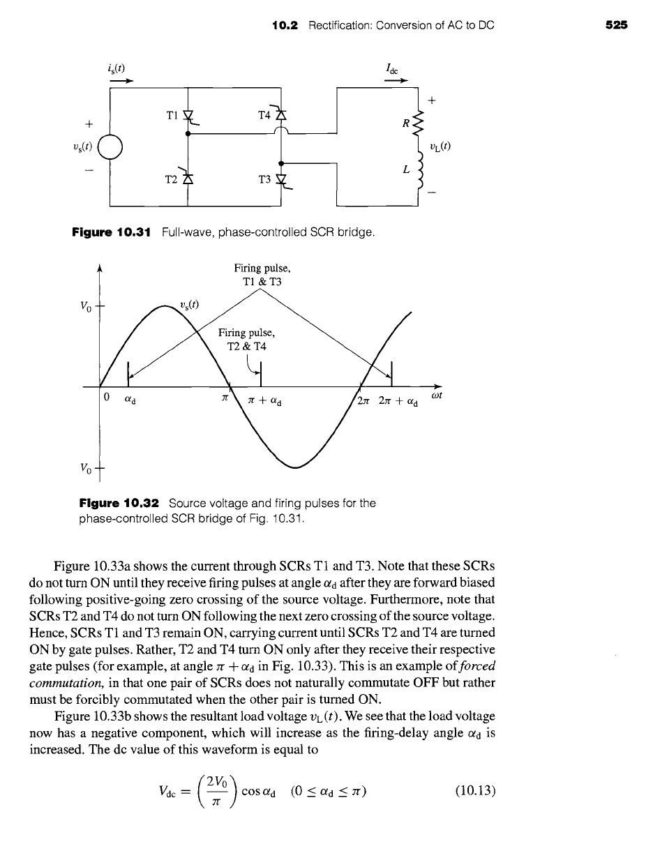
10.2.4 Single-Phase, Full.Wave,
Phase-Controlled Bridge
Figure 10.31 shows a full-wave bridge in which the diodes of Fig. 10.15 have been
replaced by SCRs. We will assume that the load inductance L is sufficiently large
that the load current is essentially constant at a dc value Idc. We will also ignore any
effects of commutating inductance, although they clearly would play the same role
in a phase-controlled rectifier system as they do in a diode-rectifier system.
Figure 10.32 shows the source voltage and the timing of the SCR gate pulses
under a typical operating condition for this circuit. Here we see that the firing pulses
are delayed by an angle c~a after the zero-crossing of the source-voltage waveform,
with the firing pulses for SCRs T 1 and T3 occuring after the positive-going transition
of
vs(t)
and those for SCRs T2 and T4 occuring after the negative-going transition.
10.2 Rectification Conversion of AC to DC 525
is(t)
+
vs ,, ()
T1 ~L
T2 ~
f
T3
Idc
+
R
VL(t)
L
Figure 10.31 Full-wave, phase-controlled SCR bridge.
Firing pulse,
T1 &T3
Vo
>
d O)t
v0
Figure 10.32 Source voltage and firing pulses for the
phase-controlled SCR bridge of Fig. 10.31.
Figure 10.33a shows the current through SCRs T1 and T3. Note that these SCRs
do not turn ON until they receive firing pulses at angle Otd after they are forward biased
following positive-going zero crossing of the source voltage. Furthermore, note that
SCRs T2 and T4 do not turn ON following the next zero crossing of the source voltage.
Hence, SCRs T1 and T3 remain ON, carrying current until SCRs T2 and T4 are turned
ON by gate pulses. Rather, T2 and T4 turn ON only after they receive their respective
gate pulses (for example, at angle Jr + Otd in Fig. 10.33). This is an example offorced
commutation, in that one pair of SCRs does not naturally commutate OFF but rather
must be forcibly commutated when the other pair is turned ON.
Figure 10.33b shows the resultant load voltage VL (t). We see that the load voltage
now has a negative component, which will increase as the firing-delay angle Otd is
increased. The dc value of this waveform is equal to
( )coso 1013