Fitzgerald A.E. Electric Machinery
Подождите немного. Документ загружается.

496 CHAPTER 10 Introduction to Power Electronics
II
Solution
a. This is a nonlinear problem in that it is not possible to write an analytic expression for
the v-i characteristic of the ideal diode. However, it can readily be solved using the
method-of-assumed-states in which, for any given value of the source voltage, the diode is
alternately assumed to be ON (a short-circuit) or OFF (an open-circuit) and the current is
found. One of the two solutions will violate the v-i characteristic of the diode (i.e., there
will be negative current flow through the short-circuit or positive voltage across the
open-circuit) and must be discarded; the remaining solution will be the correct one.
Following the above procedure, we find that the solution is given by
Vs(t) = V0 sincot Vs(t) >_ 0
VR(t) = 0 Vs(t) < 0
This voltage is plotted in Fig. 10.3b. The current is identical in form and is found simply
as iR(t) = VR(t)/R. The terminology half-wave rectification is applied to this system
because voltage is applied to the resistor during only the half cycle for which the supply
voltage waveform is positive.
b. The dc or average value of the voltage waveform is equal to
~r
oJf ~ V0
V~c = -- Vo sin (cot) dt =
and hence the dc current through the resistor is equal to
Vo
Ijc =
zrR
Calculate the average voltage across the resistor of Fig. 10.3 if the sinusoidal voltage source
of Example 10.1 is replaced by a source of the same frequency but which produces a square
wave of zero average value and peak-peak amplitude 2 V0.
Solution
Vjc =
2
10.1.2 Silicon Controlled Rectifiers and TRIACs
The characteristics of a silicon controlled rectifier, or SCR, also referred to as a
thyristor, are similar to those of a diode. However, in addition to an anode and a
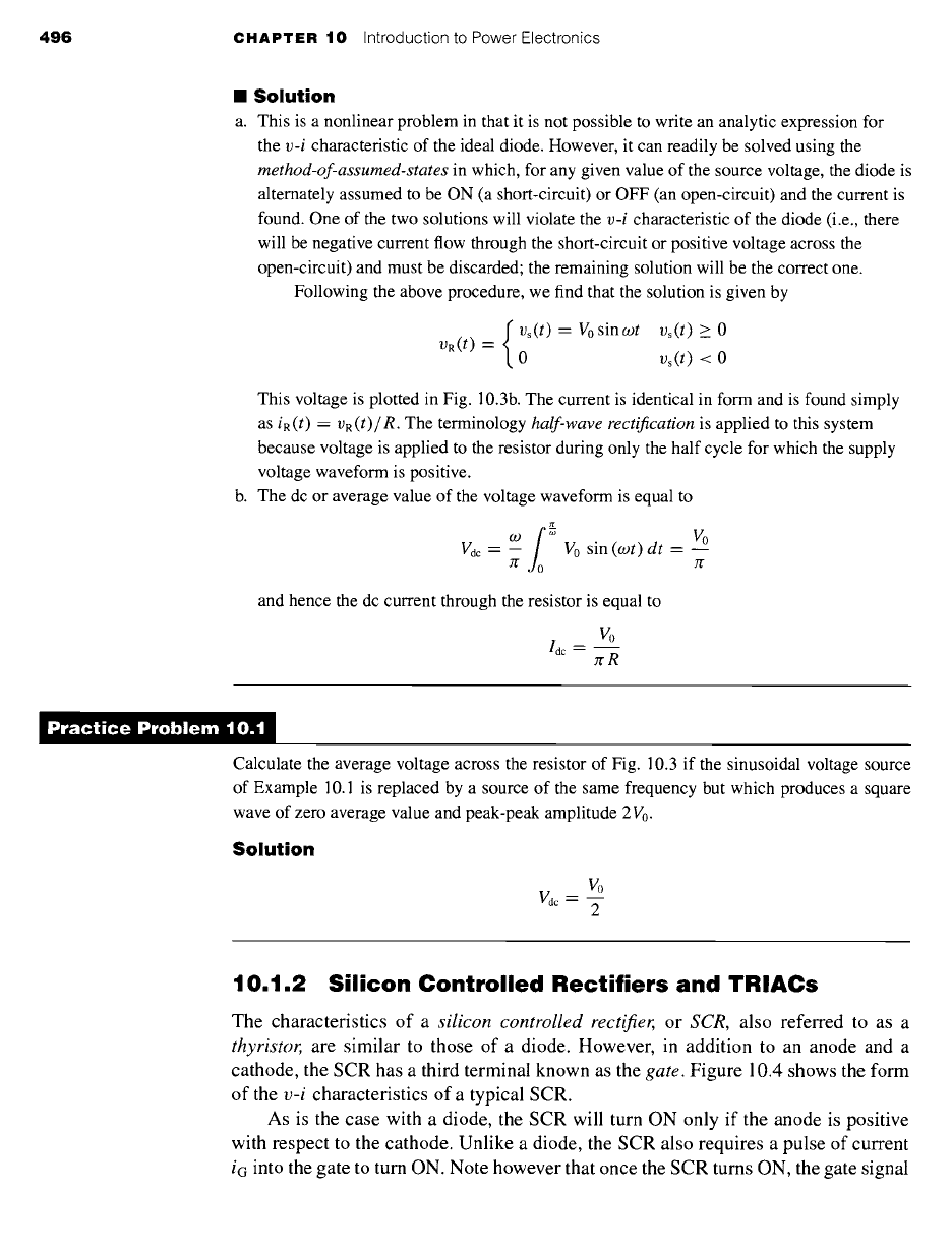
cathode, the SCR has a third terminal known as the gate. Figure 10.4 shows the form
of the v-i characteristics of a typical SCR.
As is the case with a diode, the SCR will turn ON only if the anode is positive
with respect to the cathode. Unlike a diode, the SCR also requires a pulse of current
iG into the gate to turn ON. Note however that once the SCR turns ON, the gate signal
10.1 Power Switches 497
VRB
i
ON state
I
VF
Figure 10.4
v-i
characteristic of an SCR.
v~
OFF state
~v
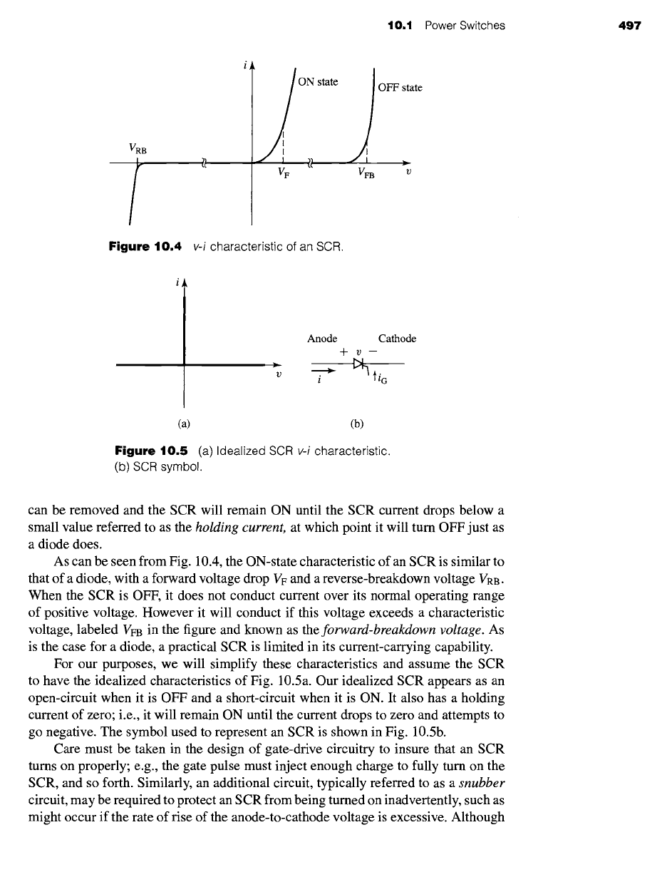
Anode Cathode
-k- v
--
i "- fiG
(a) (b)
Figure
10.5 (a) Idealized SCR
v-i
characteristic.
(b) SCR symbol.
can be removed and the SCR will remain ON until the SCR current drops below a
small value referred to as the
holding current,
at which point it will turn OFF just as
a diode does.
As can be seen from Fig. 10.4, the ON-state characteristic of an SCR is similar to
that of a diode, with a forward voltage drop VF and a reverse-breakdown voltage VRB.
When the SCR is OFF, it does not conduct current over its normal operating range
of positive voltage. However it will conduct if this voltage exceeds a characteristic
voltage, labeled VFB in the figure and known as the
forward-breakdown voltage.
As
is the case for a diode, a practical SCR is limited in its current-carrying capability.
For our purposes, we will simplify these characteristics and assume the SCR
to have the idealized characteristics of Fig. 10.5a. Our idealized SCR appears as an
open-circuit when it is OFF and a short-circuit when it is ON. It also has a holding
current of zero; i.e., it will remain ON until the current drops to zero and attempts to
go negative. The symbol used to represent an SCR is shown in Fig. 10.5b.
Care must be taken in the design of gate-drive circuitry to insure that an SCR
turns on properly; e.g., the gate pulse must inject enough charge to fully turn on the
SCR, and so forth. Similarly, an additional circuit, typically referred to as a
snubber
circuit, may be required to protect an SCR from being turned on inadvertently, such as
might occur if the rate of rise of the anode-to-cathode voltage is excessive. Although
498 CHAPTER 10 Introduction to Power Electronics
EXAMPLE 10.2
these details must be properly accounted for to achieve successful SCR performance
in practical circuits, they are not essential for the present discussion.
The basic performance of an SCR can be understood from the following example.
Consider the
half-wave rectifier
circuit of Fig. 10.6 in which a resistor R is supplied by a
voltage source
vs(t) - Vo
sin ~ot through an SCR. Note that this is identical to the circuit of
Example 10.1, with the exception that the diode has been replaced by an SCR.
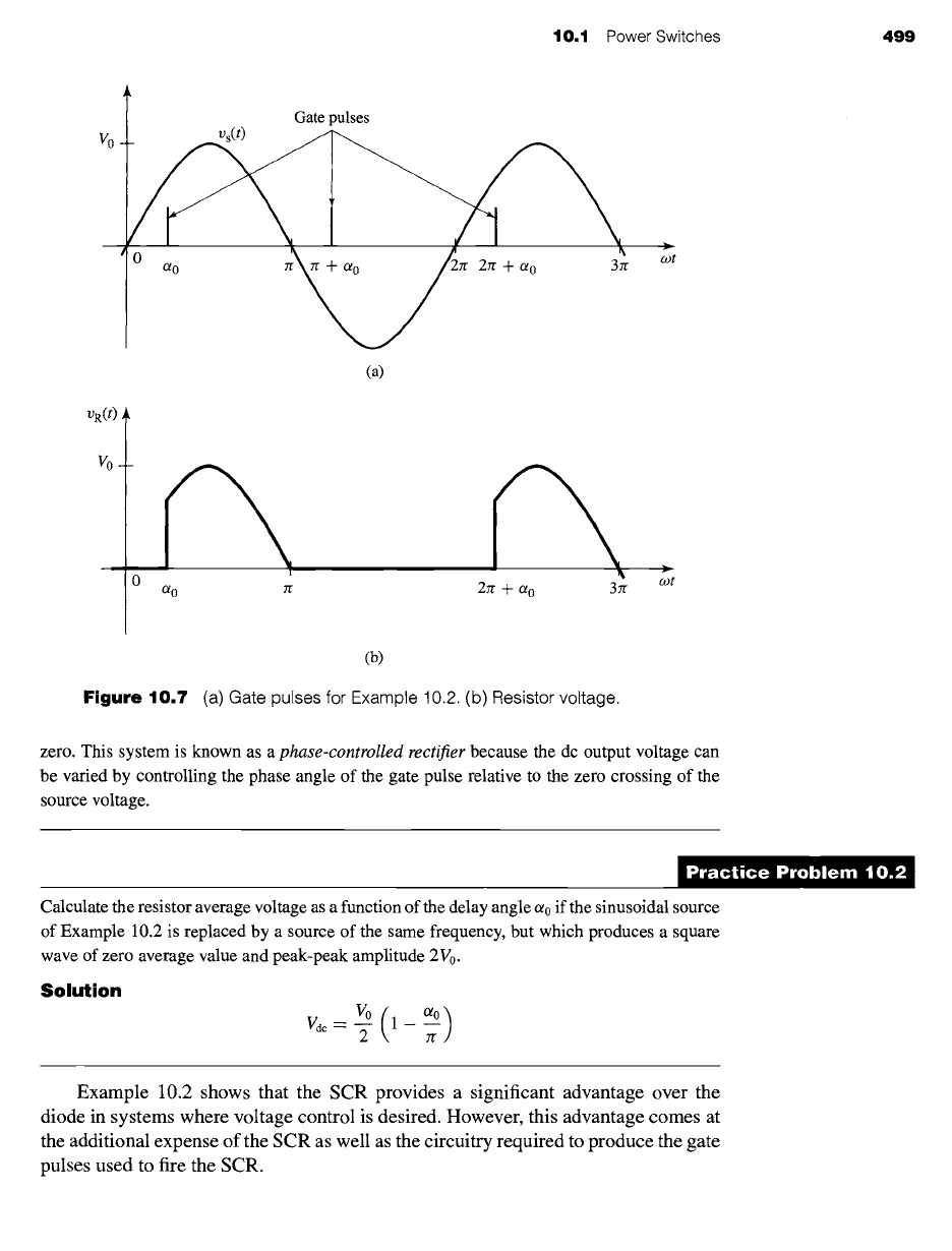
Assume that a pulse of gate current is applied to the SCR at time to (0 < to < zr/w)
following each zero-crossing of the source voltage, as shown in Fig. 10.7a. It is common to
describe this
firing-delay time
in terms of a
firing-delay angle, do - Ogto.
Find the resistor
voltage VR(t) as a function of or0. Assume the SCR to be ideal and that the gate pulses supply
sufficient charge to properly turn ON the SCR.
II Solution
The solution follows that of Example 10.1 with the exception that, independent of the polarity
of the voltage across it, once the SCR turns OFF, it will remain OFF until both the SCR voltage
becomes positive and a pulse of gate current is applied. Once a gate pulse has been applied,
the method-of-assumed-states can be used to solve for the state of the SCR.
Following the above procedure, we find the solution is given by
0
Vs(t) > 0 (prior to the gate pulse)
VR(t) "-- Vs(t) = Vo
sin
wt
Vs(t) > 0 (following the gate pulse)
0 Vs(t) < 0
This voltage is plotted in Fig. 10.7b. Note that this system produces a half-wave rectified
voltage similar to that of the diode system of Example 10.1. However, in this case, the dc value
of the rectified voltage can be controlled by controlling the timing of the gate pulse. Specifically,
it is given by
V0 ( 1 -t- cos c~0)
V~c=~
Note that when there is no delay in firing the SCR (d0 = 0), this system produces a dc
voltage of
Vo/zr,
equal to that of the diode rectifier system of Example 10.1. However, as the
gate pulse of the SCR is delayed (i.e., by increasing d0), the dc voltage can be reduced. In
fact, by delaying the gate pulse a full half cycle (c~0 = Jr) the dc voltage can be reduced to
+
v~(t) (
)
+
R __VR(t)
Figure
10.6 Half-wave SCR
rectifier circuit for Example 10.2.
Vo
Gate pulses
UR(I)
vo
10.1 Power Switches 499
(a)
r
O~ 0 7r
2zr
+
% 3zr
0 oat
(b)
Figure
10.7 (a) Gate pulses for Example 10.2. (b) Resistor voltage.
zero. This system is known as a
phase-controlled rectifier
because the dc output voltage can
be varied by controlling the phase angle of the gate pulse relative to the zero crossing of the
source voltage.
Calculate the resistor average voltage as a function of the delay angle or0 if the sinusoidal source
of Example 10.2 is replaced by a source of the same frequency, but which produces a square
wave of zero average value and peak-peak amplitude 2 V0.
Solution
0(o0)
Vac=T 1---Jr
Example 10.2 shows that the SCR provides a significant advantage over the
diode in systems where voltage control is desired. However, this advantage comes at
the additional expense of the SCR as well as the circuitry required to produce the gate
pulses used to fire the SCR.
500 CHAPTER 10 Introduction to Power Electronics
EXAMPLE 10.3
OFF state
ON state
Jr- V B
~fi G
(a) (b)
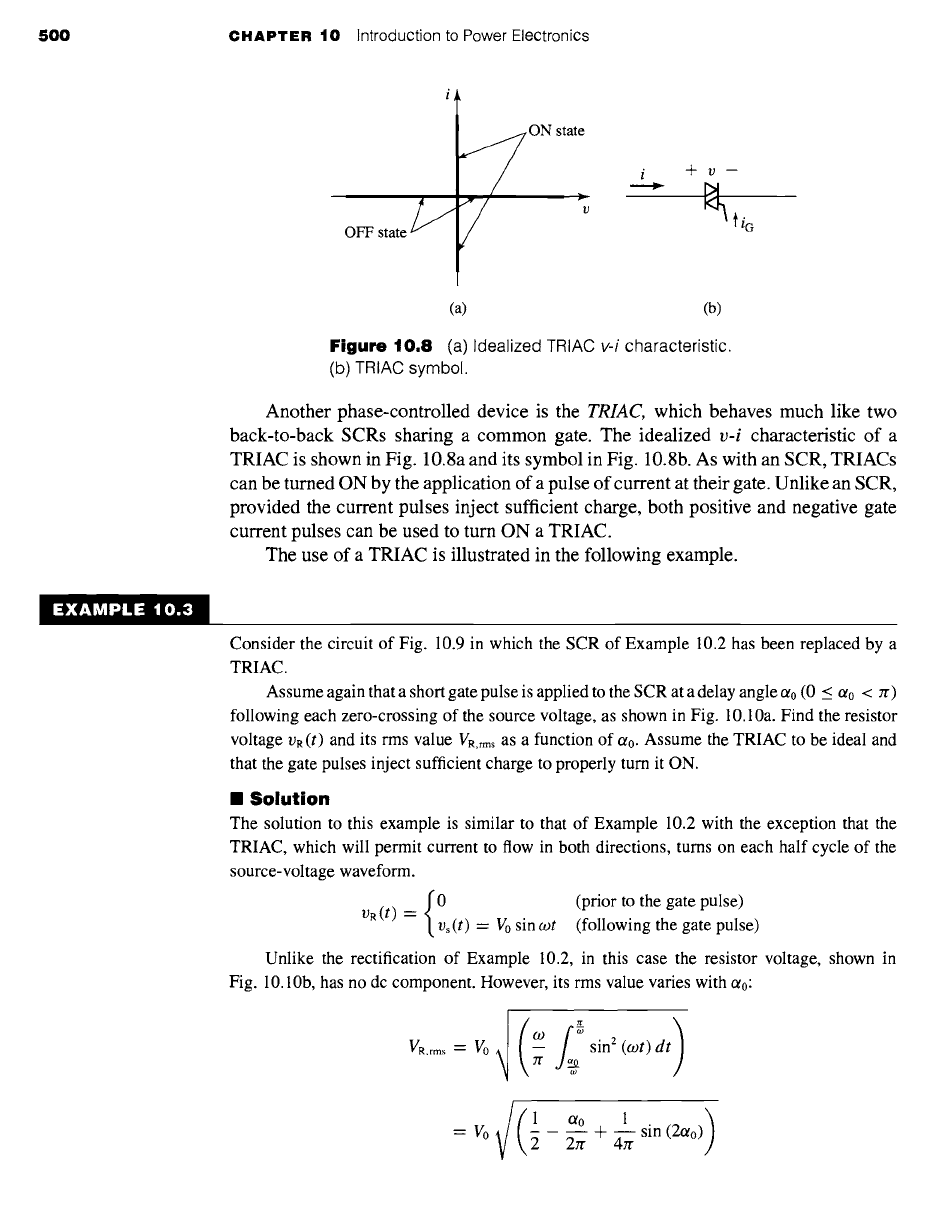
Figure
10.8 (a) Idealized TRIAC
v-i
characteristic.
(b) TRIAC symbol.
Another phase-controlled device is the
TRIAC,
which behaves much like two
back-to-back SCRs sharing a common gate. The idealized
v-i
characteristic of a
TRIAC is shown in Fig. 10.8a and its symbol in Fig. 10.8b. As with an SCR, TRIACs
can be turned ON by the application of a pulse of current at their gate. Unlike an SCR,
provided the current pulses inject sufficient charge, both positive and negative gate
current pulses can be used to turn ON a TRIAC.
The use of a TRIAC is illustrated in the following example.
Consider the circuit of Fig. 10.9 in which the SCR of Example 10.2 has been replaced by a
TRIAC.
Assume again that a short gate pulse is applied to the SCR at a delay angle ct0 (0 < ct0 < Jr)
following each zero-crossing of the source voltage, as shown in Fig. 10.10a. Find the resistor
voltage VR (t) and its rms value VR.rms as a function of ct0. Assume the TRIAC to be ideal and
that the gate pulses inject sufficient charge to properly turn it ON.
II Solution
The solution to this example is similar to that of Example 10.2 with the exception that the
TRIAC, which will permit current to flow in both directions, turns on each half cycle of the
source-voltage waveform.
f0 (prior to the gate pulse)
OR(t)
vs(t) = Vo
sin rot (following the gate pulse)
Unlike the rectification of Example 10.2, in this case the resistor voltage, shown in
Fig. 10.10b, has no dc component. However, its rms value varies with c~0:
VR
.... --
V0 -- sin 2
(wt) dt
7l"
= Vo 2 27r + ~ sin (2ao)
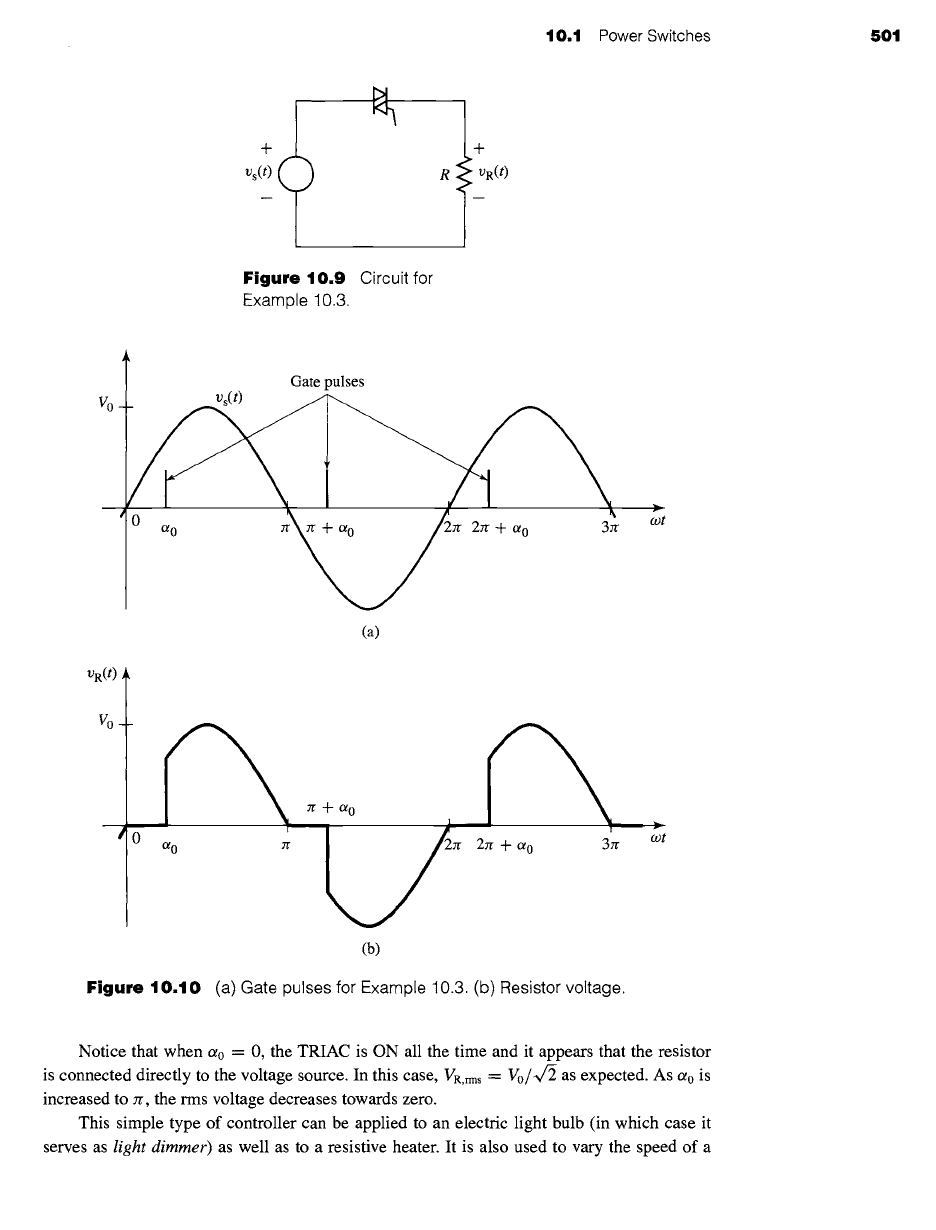
10.1 Power Switches S01
)
Figure 10.9
Circuit for
Example 10.3.
+
Vs(t) (
l Gate pulses
v0
+
R __VR(t)
(a)
VR(t)
Vo
Ot 0
rr+c~ o
i
0 Jr
2zr + ot 0 3zr
cot
(b)
Figure
10.10 (a) Gate pulses for Example 10.3. (b) Resistor voltage.
Notice that when or0 = 0, the TRIAC is ON all the time and it appears that the resistor
is connected directly to the voltage source. In this case, VR,rms --
Vo/~
as expected. As or0 is
increased to Jr, the rms voltage decreases towards zero.
This simple type of controller can be applied to an electric light bulb (in which case it
serves as
light dimmer)
as well as to a resistive heater. It is also used to vary the speed of a
502 CHAPTER 10 Introduction to Power Electronics
universal motor and finds widespread application as a speed-controller in small ac hand tools,
such as hand drills, as well as in small appliances, such as electric mixers, where continuous
speed variation is desired.
~ractice Problem 10.;
Find the rms resistor voltage for the system of Example 10.3 if the sinusoidal source has been
replaced by a source of the same frequency but which produces a square wave of zero average
value and peak-peak amplitude 2 V0.
Solution
VR'rms = V° V/(1 - c~°) zr
10.1.3 Transistors
For power-electronic circuits where control of voltages and currents is required,
power transistors have become a common choice for the controllable switch. Al-
though a number of types are available, we will consider only two: the
metal-
oxide-semiconductor field effect transistor (MOSFET)
and the
insulated-gate bipolar
transistor (IGBT).
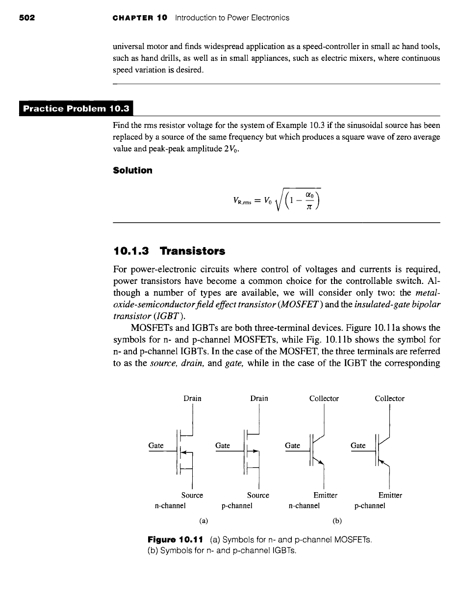
MOSFETs and IGBTs are both three-terminal devices. Figure 10.11 a shows the
symbols for n- and p-channel MOSFETs, while Fig. 10.1 l b shows the symbol for
n- and p-channel IGBTs. In the case of the MOSFET, the three terminals are referred
to as the
source, drain,
and
gate,
while in the case of the IGBT the corresponding
Gate
Drain
Source
n-channel
Gate
Drain
Source
p-channel
Gate
Collector
Emitter
n-channel
(a) (b)
Gate
Collector
Emitter
p-channel
Figure
10.11 (a) Symbols for n- and p-channel MOSFETs.
(b) Symbols for n- and p-channel IGBTs.
10.1 Power Switches 503
terminals are the
emitter, collector,
and
gate.
For the MOSFET, the control signal
is the gate-source voltage, vGS. For the IGBT, it is the gate-emitter voltage, VGE. In
both the MOSFET and the IGBT, the gate electrode is capacitively coupled to the
remainder of the device and appears as an open circuit at dc, drawing no current, and
drawing only a small capacitive current under ac operation.
Figure 10.12a shows the
v-i
characteristic of a typical n-channel MOSFET. The
characteristic of the corresponding p-channel device looks the same, with the ex-
ception that the signs of the voltages and the currents are reversed. Thus, in an
n-channel device, current flows from the drain to the source when the drain-source and
(VDs)RB
Ohmic
>;<
I
!
J / (VGS- VT) -- VDS
Active
VGS
I 0 \Vcs_ < VT
(a)
J
__..J
J
Zl I >
(%S)FB
VDs
(VcE)RB
(
, \
0 (VCE)sat VG E _< VT
VGE
(b)
J
J
J
J
J
zz
I
(VcE)FB
Figure 10.12 (a)
Typical
v-i
characteristic for an n-channel MOSFET.
(b) Typical
v-i
characteristic for an n-channel IGBT.
1)CE
504 CHAPTER 10 Introduction to Power Electronics
gate-source voltages are positive, while in a p-channel device current flows from the
source to the drain when the drain-source and gate-source voltages are negative.
Note the following features of the MOSFET and IGBT characteristics:
m In the case of the MOSFET, for positive drain-source voltage vDS, no drain
current will flow for values of VGS less than a
threshold voltage
which we will
refer to by the symbol VT. Once vGS exceeds VT, the drain current iD increases
as VGS is increased.
In the case of the IGBT, for positive collector-emitter voltage vCE, no
collector current will flow for values of VGE less than a threshold voltage VT.
Once VGE exceeds VT, the collector current ic increases as VGE is increased.
l In the case of the MOSFET, no drain current flows for negative drain-source
voltage.
In the case of the IGBT, no collector current flows for negative collector-
emitter voltage.
m Finally, the MOSFET will fail if the drain-source voltage exceeds its
breakdown limits; in Fig. 10.12a, the forward breakdown voltage is indicated
by the symbol (VDS)FB while the reverse breakdown voltage is indicated by the
symbol ( VDS)RB.
Similarly, the IGBT will fail if the collector-emitter voltage exceeds its
breakdown values; in Fig. 10.12b, the forward breakdown voltage is indicated
by the symbol (VcE)FB while the reverse breakdown voltage is indicated by the
symbol (VcE)R B .
m Although not shown in the figure, a MOSFET will fail due to excessive
gate-source voltage as well as excessive drain current which leads to excessive
power dissipation in the device. Similarly an IGBT will fail due to excessive
gate-emitter voltage and excessive collector current.
Note that for small values of 1)CE , the IGBT voltage approaches a constant value,
independent of the drain current. This
saturation voltage,
labeled (
VCE)sat
in the figure,
is on the order of a volt or less in small devices and a few volts in high-power devices.
Correspondingly, in the MOSFET, for small values of Vos, VDS is proportional to the
drain current and the MOSFET behaves as a small resistance whose value decreases
with increasing vGS.
Fortunately, for our purposes, the details of these characteristics are not impor-
tant. As we will see in the following example, with a sufficient large gate signal, the
voltage drop across both the MOSFET and the IGBT can be made quite small. In this
case, these devices can be modeled as a short circuit between the drain and the source
in the case of the MOSFET and between the collector and the emitter in the case
of the IGBT. Note, however, these "switches" when closed carry only unidirectional
current, and hence we will model them as a switch in series with an ideal diode. This
ideal-switch model
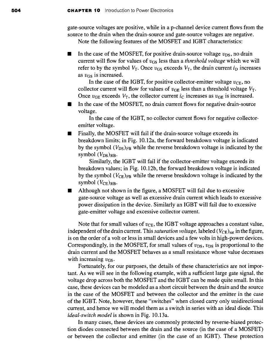
is shown in Fig. 10.13a.
In many cases, these devices are commonly protected by reverse-biased protec-
tion diodes connected between the drain and the source (in the case of a MOSFET)
or between the collector and emitter (in the case of an IGBT). These protection
10.1 Power Switches 505
G,B
0
D,C D,C
o---- /
IT
S,E S,E
(a) (b)
Figure 10.13 (a)
Ideal-switch model for a MOSFET or
an IGBT showing the series ideal diode which represents
the unidirectional-current device characteristic.
(b) Ideal-switch model for devices which include a
reverse-biased protection diode. The symbols G, D, and
S apply to the MOSFET while the symbols B, C, and E
apply to the IBGT.
devices are often included as integral components within the device package. If these
protection diodes are included, there is actually no need to include the series diode,
in which case the model can be reduced to that of Fig. 10.13b.
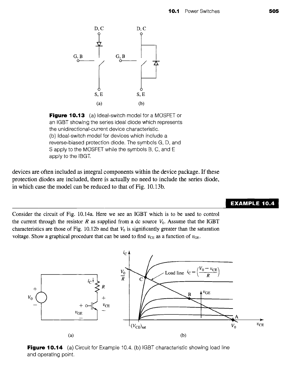
Consider the circuit of Fig. 10.14a. Here we see an IGBT which is to be used to control
the current through the resistor R as supplied from a dc source V0. Assume that the IGBT
characteristics are those of Fig. 10.12b and that V0 is significantly greater than the saturation
voltage. Show a graphical procedure that can be used to find VCE as a function of V~E.
EXAMPLE 10.4
+
)
ic}
R
+
VGE
R
(VCE)sat
Coa ,ine i _
(a) (b)
VGE
"'-LA
vo
Figure 10.14 (a)
Circuit for Example
10.4. (b)
IGBT characteristic showing load line
and operating point.
r
VCE