Fitzgerald A.E. Electric Machinery
Подождите немного. Документ загружается.

506 CHAPTER 10 Introduction to Power Electronics
II
Solution
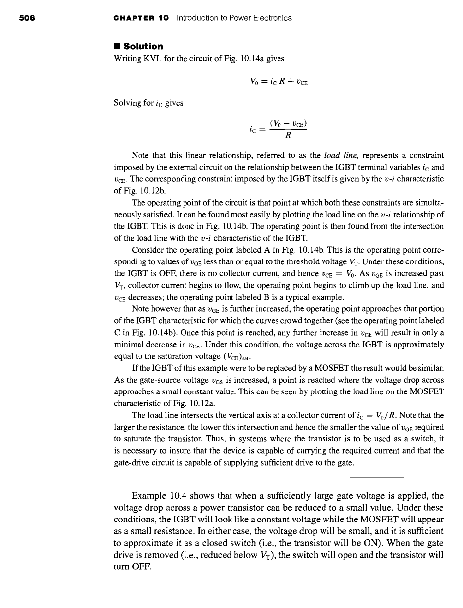
Writing KVL for the circuit of Fig. 10.14a gives
V0 = ic R +
UCE
Solving for ic gives
iC ---
(Vo- Vc~.)
Note that this linear relationship, referred to as the
load line,
represents a constraint
imposed by the external circuit on the relationship between the IGBT terminal variables ic and
VCE. The corresponding constraint imposed by the IGBT itself is given by the
v-i
characteristic
of Fig. 10.12b.
The operating point of the circuit is that point at which both these constraints are simulta-
neously satisfied. It can be found most easily by plotting the load line on the
v-i
relationship of
the IGBT. This is done in Fig. 10.14b. The operating point is then found from the intersection
of the load line with the
v-i
characteristic of the IGBT.
Consider the operating point labeled A in Fig. 10.14b. This is the operating point corre-
sponding to values of VGE less than or equal to the threshold voltage VT. Under these conditions,
the IGBT is OFF, there is no collector current, and hence VCE = V0. As VGE is increased past
VT, collector current begins to flow, the operating point begins to climb up the load line, and
VCE decreases; the operating point labeled B is a typical example.
Note however that as VGE is further increased, the operating point approaches that portion
of the IGBT characteristic for which the curves crowd together (see the operating point labeled
C in Fig. 10.14b). Once this point is reached, any further increase in VGE will result in only a
minimal decrease in VCE. Under this condition, the voltage across the IGBT is approximately
equal to the saturation voltage
(VCE)sat.
If the IGBT of this example were to be replaced by a MOSFET the result would be similar.
As the gate-source voltage Vcs is increased, a point is reached where the voltage drop across
approaches a small constant value. This can be seen by plotting the load line on the MOSFET
characteristic of Fig. 10.12a.
The load line intersects the vertical axis at a collector current of ic --
Vo/R.
Note that the
larger the resistance, the lower this intersection and hence the smaller the value of VGE required
to saturate the transistor. Thus, in systems where the transistor is to be used as a switch, it
is necessary to insure that the device is capable of carrying the required current and that the
gate-drive circuit is capable of supplying sufficient drive to the gate.
Example 10.4 shows that when a sufficiently large gate voltage is applied, the
voltage drop across a power transistor can be reduced to a small value. Under these
conditions, the IGBT will look like a constant voltage while the MOSFET will appear
as a small resistance. In either case, the voltage drop will be small, and it is sufficient
to approximate it as a closed switch (i.e., the transistor will be ON). When the gate
drive is removed (i.e., reduced below VT), the switch will open and the transistor will
turn OFE
10.2 Rectification Conversion of AC to DC 507
10.2 RECTIFICATION: CONVERSION
OF AC TO DC
The power input to many motor-drive systems comes from a constant-voltage,
constant-frequency source (e.g., a 50- or 60-Hz power system), while the output must
provide variable-voltage and/or variable-frequency power to the motor. Typically such
systems convert power in two stages: the input ac is first
rectified
to dc, and the dc
is then converted to the desired ac output waveform. We will thus begin with a dis-
cussion of rectifier circuits. We will then discuss inverters, which convert dc to ac, in
Section 10.3.
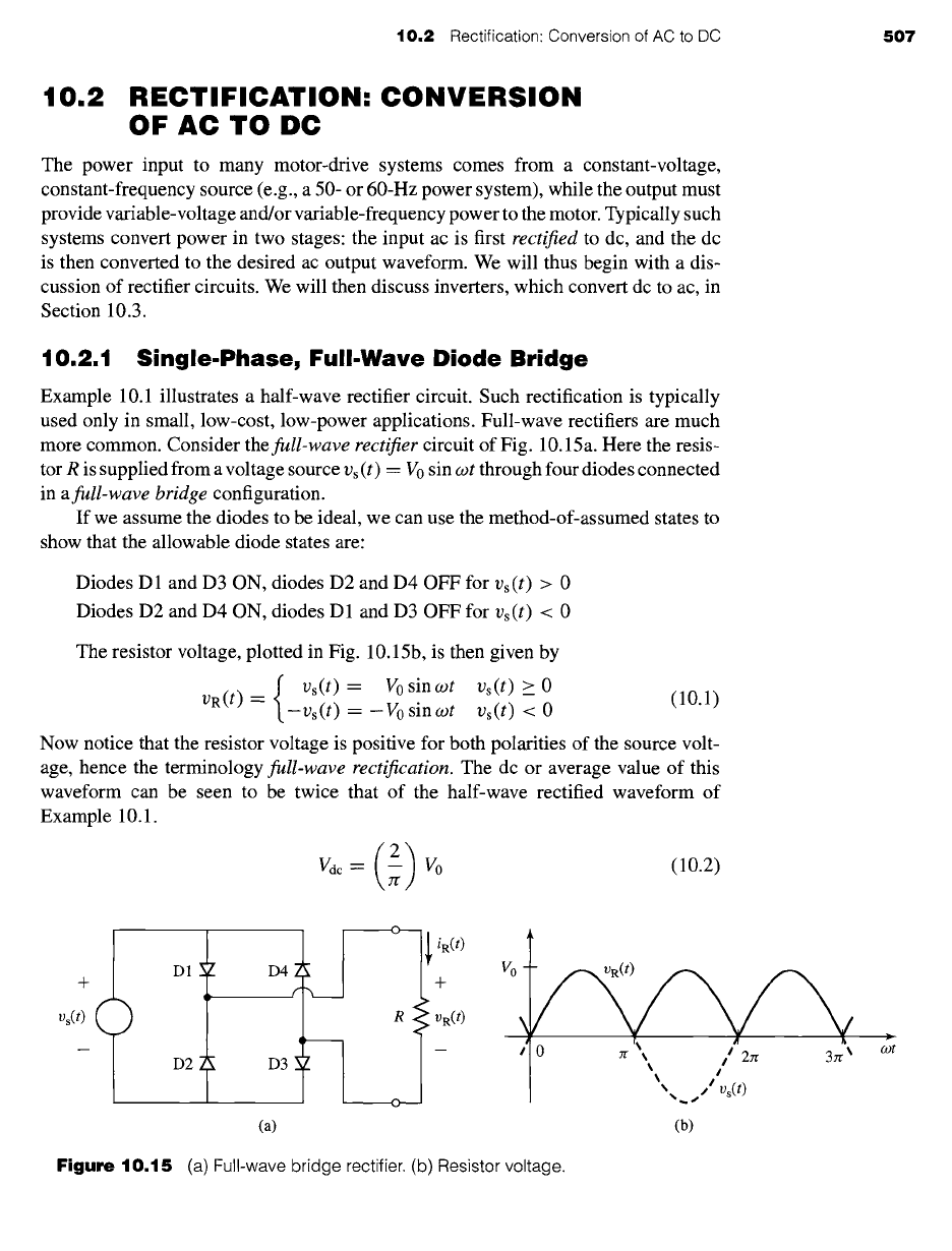
10.2.1 Single-Phase, Full-Wave Diode Bridge
Example 10.1 illustrates a half-wave rectifier circuit. Such rectification is typically
used only in small, low-cost, low-power applications. Full-wave rectifiers are much
more common. Consider the
full-wave rectifier
circuit of Fig. 10.15a. Here the resis-
tor R is supplied from a voltage source Vs (t) = V0 sin cot through four diodes connected
in
a full-wave bridge
configuration.
If we assume the diodes to be ideal, we can use the method-of-assumed states to
show that the allowable diode states are:
Diodes D1 and D3 ON, diodes D2 and D4 OFF for Vs(t) > 0
Diodes D2 and D4 ON, diodes D1 and D3 OFF for Vs(t) < 0
The resistor voltage, plotted in Fig. 10.15b, is then given by
Vs(t)- V0sincot Vs(t)>_O
VR(t) -- --Vs(t) = -V0sincot Vs(t) < 0 (10.1)
Now notice that the resistor voltage is positive for both polarities of the source volt-
age, hence the terminology
full-wave rectification.
The dc or average value of this
waveform can be seen to be twice that of the half-wave rectified waveform of
Example 10.1.
Vdc = (2) V0 (10.2)
+
Vs(t) (
)
D1 ~ D4
D2 D3
(a)
VR(t)
m
Vo
/]U zr "~ / 2~
3zr ~
/
[ "xxx,. ,,/'~s(t)
(b)
Figure 10.15 (a) Full-wave bridge rectifier. (b) Resistor voltage.
r
ogt
508 CHAPTER
10 Introduction to Power Electronics
The rectified waveforms of Figs. 10.3b and 10.15b are clearly not the sort of
"dc" waveforms that are considered desirable for most applications. Rather, to be
most useful, the rectified dc should be relatively constant and ripple free. Such a
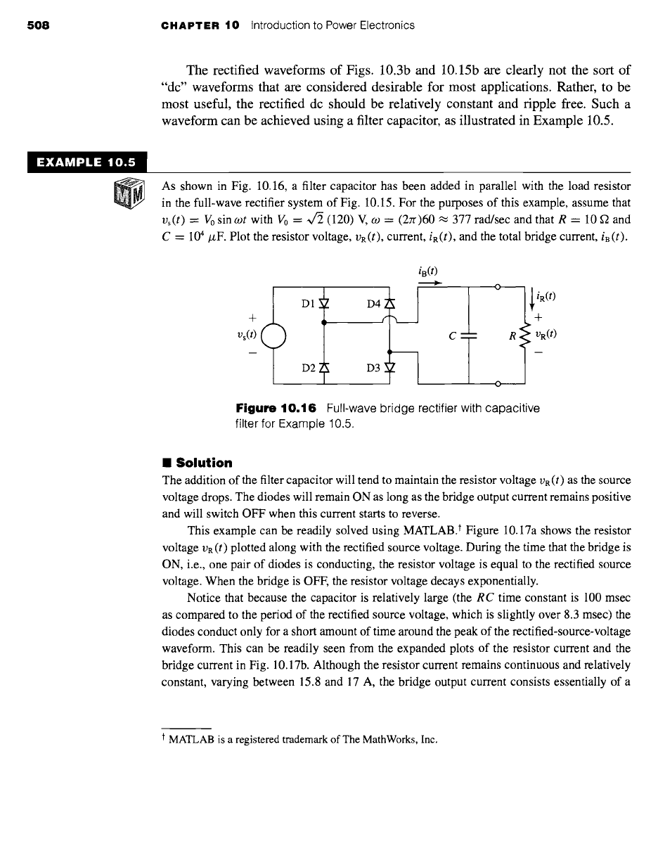
waveform can be achieved using a filter capacitor, as illustrated in Example 10.5.
As shown in Fig. 10.16, a filter capacitor has been added in parallel with the load resistor
in the full-wave rectifier system of Fig. 10.15. For the purposes of this example, assume that
Vs(t) = V0 sincot with V0 = ~/~ (120) V, co = (2zr)60 ~ 377 rad/sec and that R = 10 f2 and
C
-- 10 4/.zF.
Plot the resistor voltage, VR(t), current, iR(t), and the total bridge current, iB(t).
+
Vs(t) Q
-I
D21 D3 @
iB(t)
c!
Figure 10.16
Full-wave bridge rectifier with capacitive
filter for Example 10.5.
II
Solution
The addition of the filter capacitor will tend to maintain the resistor voltage VR (t) as the source
voltage drops. The diodes will remain ON as long as the bridge output current remains positive
and will switch OFF when this current starts to reverse.
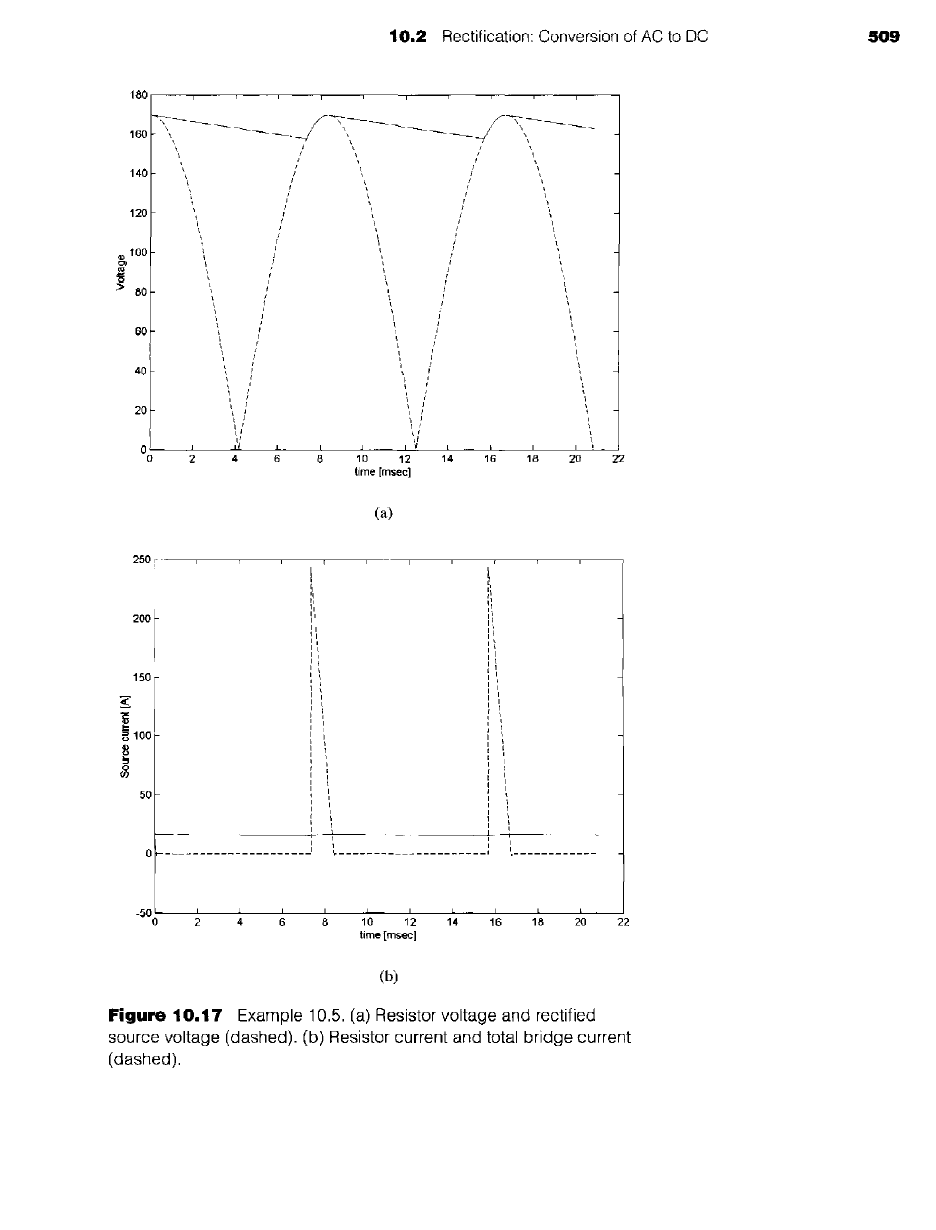
This example can be readily solved using MATLAB. t Figure 10.17a shows the resistor
voltage OR (t) plotted along with the rectified source voltage. During the time that the bridge is
ON, i.e., one pair of diodes is conducting, the resistor voltage is equal to the rectified source
voltage. When the bridge is OFF, the resistor voltage decays exponentially.
Notice that because the capacitor is relatively large (the
R C
time constant is 100 msec
as compared to the period of the rectified source voltage, which is slightly over 8.3 msec) the
diodes conduct only for a short amount of time around the peak of the rectified-source-voltage
waveform. This can be readily seen from the expanded plots of the resistor current and the
bridge current in Fig. 10.17b. Although the resistor current remains continuous and relatively
constant, varying between 15.8 and 17 A, the bridge output current consists essentially of a
t MATLAB is a registered trademark of The MathWorks, Inc.
O0
~c
<
o ,,A
~P
x
o
co
.
~~ ~
,--v
o~ ~
~-~. o~
,-~ <
o__ ~=
~Q
0 ~ 0~
,-e-
CT Q-
"-,. --,
o
c Q-
o
I-
I
L
i
i
i
i
i
i
i
'I
l__J
Source current [A]
¢.n o o~ o o-i
o o o o o
i i i i
Voltage
I,,O ¢=, o3 o> o IX.) -I~ o3 oo
o o o o o o o o o o
o i i i i I i i
t
;:n
I~
I I I i I I I I

510 CHAPTER
10 Introduction to Power Electronics
current pulse which flows for less than 0.9 msec near the peak of the rectified voltage waveform
and has a peak value of 250 A. It should be pointed out that the peak current in a practical
circuit will be smaller than 250 A, being limited by circuit impedances, diode drops, and so on.
Using MATLAB, it is possible to calculate the rms value of the resistor current to be
16.4 A while that of the bridge current is 51.8 A. We see therefore that the bridge diodes in
such a system must be rated for rms currents significantly in excess of that of the load. The data
sheets for power-supply diodes typically indicate their rms current ratings, specifically with
these sorts of applications in mind. Such peaked supply currents are characteristic of rectifier
circuits with capacitive loads and can significantly affect the voltage waveforms on ac power
systems when they become a significant fraction of the overall system load.
The
ripple voltage
in the resistor voltage is defined as the difference between its maximum
and minimum values. In this example, the maximum value is equal to the peak value of the source
voltage, or 169.7 V. The minimum value can be found from the MATLAB solution to be 157.8 V.
Thus the ripple voltage is 11.9 V. Clearly the ripple voltage can be decreased by increasing the
value of the filter capacitor. Note however that this comes at the expense of increased cost as
well as shorter current pulses and higher rms current through the rectifier diodes.
Here is the MATLAB script for Example 10.5.
clc
clear
%parameters
omega = 2"pi'60;
R = I0;
C = 0.01;
V0 = 120*sqrt(2) ;
tau : R'C;
Nmax = 800;
% diode = 1 when rectifier bridge is conducting
diode = 1 ;
%Here is the loop that does the work.
for n = l:Nmax+l
t(n) = (2.5*pi/omega)*(n-1)/Nmax; %time
vs(n) = V0*cos(omega*t(n) ) ; %source voltage
vrect(n) = abs(vs(n) ) ; %full-wave rectified source voltage
%Calculations if the rectifier bridge is ON
if diode == 1
%If the bridge is ON, the resistor voltage is equal to the rectified
%source voltage.
vm(n) = vrect(n) ;
%Check the total current out of rectifiers
if (omega*t(n)) <= pi/2.
iB(n) = vR(n) /R - V0*C*omega*sin(omega*t(n) ) ;
elseif (omega*t(n)) <= 3.*pi/2.

b ~ ~J ~ ~ ~ N ~J
o\O
~J ~h ~ ~ ~ ~ ~ N ~ o\O ~. o\O CD (I) Q~ ~- ~- <
o\O o\O
CD
< r~ ~
~. o\O (1) ~. ~ ~.
0 ~ 0 N ~ ~ ~ ~ ~ ~J 0 ~ 0 N ~ ~ ~ ~ ~ (D ~ ~ ~- ~ b~ ~ (1) :~ ~ 0 0 ~- ~ H ~ t~ ~ t~
0 ~ ~- ~ ~ 0 0 C H ~ 0 ~ ~- ~ ~ 0 0 ~ ~ Q~ 0 ---- --- N ~ ~ ~ ~ 0 h~ ~ .---. In .--.
~- ~ cn ~ ~Y ~ ~ ~n ~- ~ ~- ~ cn ~Y b ~ ~- :~ li ~ ~) ~ .---.. ~ ~ ~ ~ ~) h~ ~ 0-, ~" ~ ~)
0
o ~
o -. -.. o 0 .---. o o -., -. o 0 ~ ~
~ ~ o ~- 15 o < ~- o ~- ~ ~
bo O ~- ~- ~- bo O ~- ~- -.. (1)
- H d) - ~ SS . ct ~ - ~ o'-
-. o ~1 -.---, r.n ~ ~ ~ ~ -..-~ r.n
..,. Q co !D (1 co ~
bo c; (I) ~ ~ cr o ~ (D ~
(1)
Q~
ct
~ 0
FJ.
(1) 0
cr
i~. (1)
• - "
0
~- 0
fD
®
O~
<
fD
g~
P~
®
P~
(I)
H ~ r~
II CD II II CD ~ CD II ~ CD
"-"
~ ~ 0
~ -.
o ~ ~
i ,~ ~ (I:) ~ o' ~
~ ~ ~ ~ +
i-'-
o'- g~ o o
0
V "---" ~n 0 ~. ~.
i
LQ 0 0
0 ~ ~ 0 ~
-. 0 b ~ CD (D
(I) !D ~ Co
ct In ct ~. ~.
C; r.n < .-.. ..-..
"4 ~" (1) 0 0
"" o - ~
ID i-,- .----. ---
~" ~ "--4 ~_.
0 ~ ....
0 ~_~
~r
0
512
CHAPTER 10 Introduction to Power Electronics
Practice Problem 10.,
Use MATLAB to calculate the ripple voltage and rms diode current for the system of Exam-
ple 10.5 for (a) C = 5 x 10⁴/zF and (b) C = 5 x 10³/zF. (Hint: Note that the rms current must
be calculated over an integral number of cycles of the current waveform).
Solution
a. 2.64 V and 79.6 Arms
b. 21.6 V and 42.8 Arms
In Example 10.5 we have seen that a capacitor can significantly decrease the
ripple voltage across a resistive load. However, this comes at the cost of large bridge
current pulses since the current must be delivered to the capacitor in the short time
period during which the rectified source voltage is near its peak value.
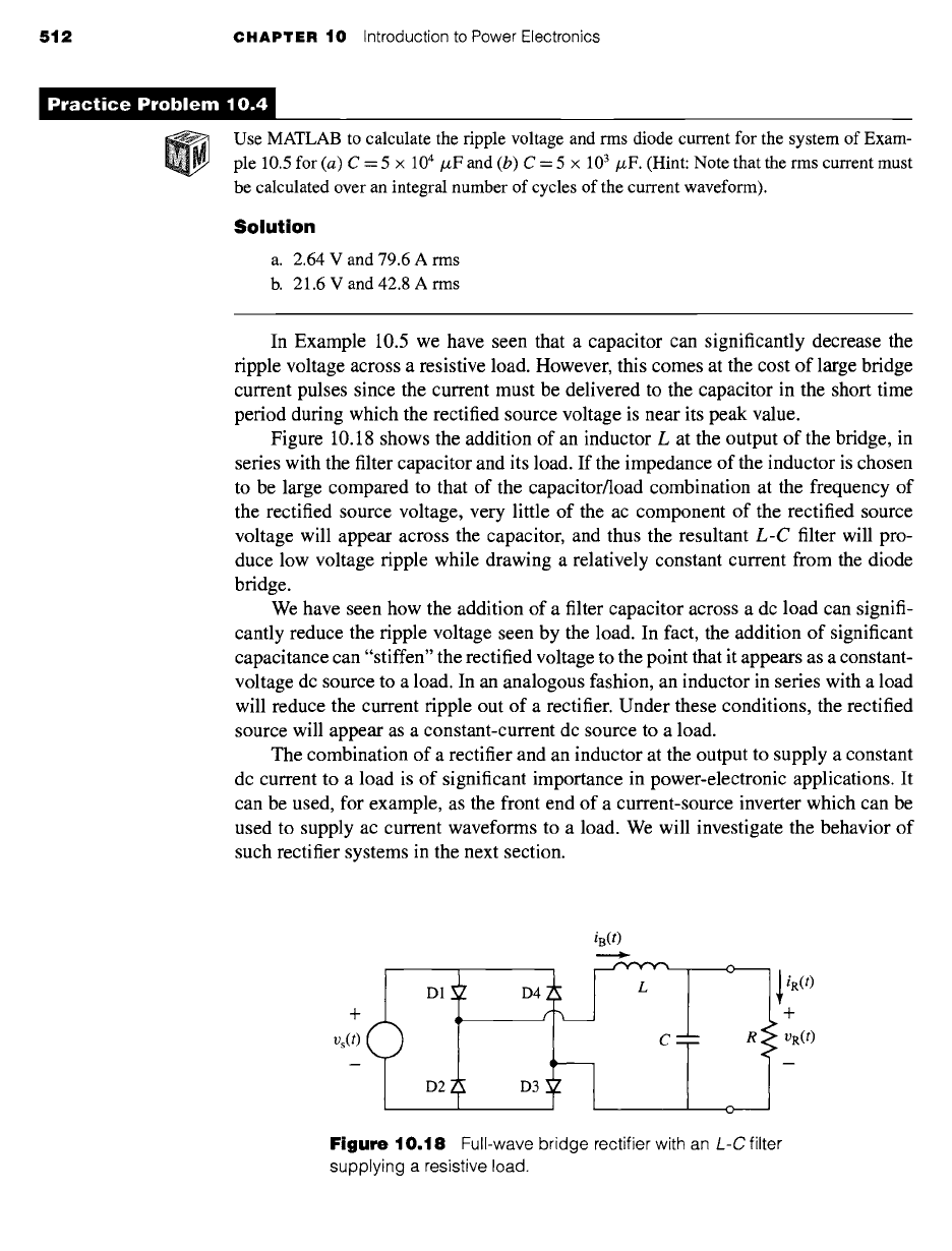
Figure 10.18 shows the addition of an inductor L at the output of the bridge, in
series with the filter capacitor and its load. If the impedance of the inductor is chosen
to be large compared to that of the capacitor/load combination at the frequency of
the rectified source voltage, very little of the ac component of the rectified source
voltage will appear across the capacitor, and thus the resultant
L-C
filter will pro-
duce low voltage ripple while drawing a relatively constant current from the diode
bridge.
We have seen how the addition of a filter capacitor across a dc load can signifi-
cantly reduce the ripple voltage seen by the load. In fact, the addition of significant
capacitance can "stiffen" the rectified voltage to the point that it appears as a constant-
voltage dc source to a load. In an analogous fashion, an inductor in series with a load
will reduce the current ripple out of a rectifier. Under these conditions, the rectified
source will appear as a constant-current dc source to a load.
The combination of a rectifier and an inductor at the output to supply a constant
dc current to a load is of significant importance in power-electronic applications. It
can be used, for example, as the front end of a current-source inverter which can be
used to supply ac current waveforms to a load. We will investigate the behavior of
such rectifier systems in the next section.
+
Vs(t)
D2 1 D3
iB(t)
* l
C~
&~_~ R(t)
R I o?(t)
Figure 10.18
Full-wave bridge rectifier with an
L-C
filter
supplying a resistive load.
10.2 Rectification: Conversion of AC to DC 513
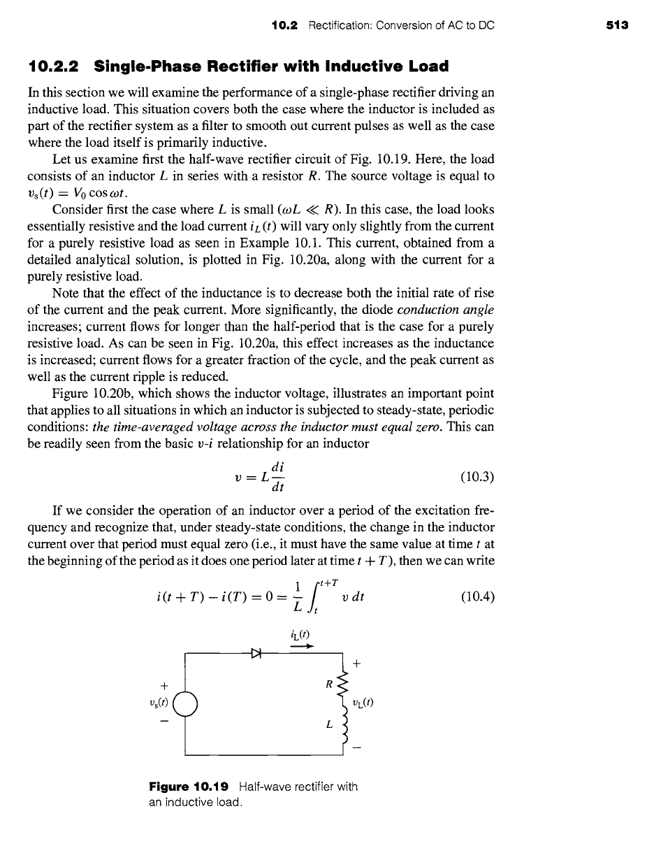
10.2.2 Single-Phase Rectifier with Inductive Load
In this section we will examine the performance of a single-phase rectifier driving an
inductive load. This situation covers both the case where the inductor is included as
part of the rectifier system as a filter to smooth out current pulses as well as the case
where the load itself is primarily inductive.
Let us examine first the half-wave rectifier circuit of Fig. 10.19. Here, the load
consists of an inductor L in series with a resistor R. The source voltage is equal to
Vs(t) = V0 cos o)t.
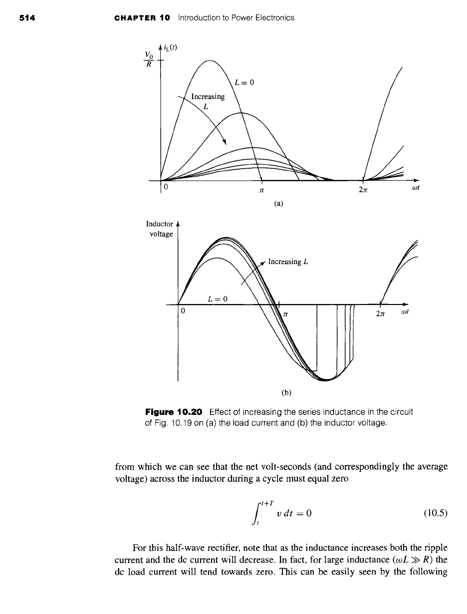
Consider first the case where L is small (wL << R). In this case, the load looks
essentially resistive and the load current iL (t) will vary only slightly from the current
for a purely resistive load as seen in Example 10.1. This current, obtained from a
detailed analytical solution, is plotted in Fig. 10.20a, along with the current for a
purely resistive load.
Note that the effect of the inductance is to decrease both the initial rate of rise
of the current and the peak current. More significantly, the diode
conduction angle
increases; current flows for longer than the half-period that is the case for a purely
resistive load. As can be seen in Fig. 10.20a, this effect increases as the inductance
is increased; current flows for a greater fraction of the cycle, and the peak current as
well as the current ripple is reduced.
Figure 10.20b, which shows the inductor voltage, illustrates an important point
that applies to all situations in which an inductor is subjected to steady-state, periodic
conditions:
the time-averaged voltage across the inductor must equal zero.
This can
be readily seen from the basic
v-i
relationship for an inductor
di
v = L-- (10.3)
dt
If we consider the operation of an inductor over a period of the excitation fre-
quency and recognize that, under steady-state conditions, the change in the inductor
current over that period must equal zero (i.e., it must have the same value at time t at
the beginning of the period as it does one period later at time t + T), then we can write
1
ft+T
-- vdt
i(t + T)-i(T)--O= L at
(10.4)
iL(t)
+
+ R
Vs(t) VL(t)
-- L
Figure 10.19
Half-wave rectifier with
an inductive load.
514 CHAPTER 10 Introduction to Power Electronics
V0
R
iL(t)
0 7g
(a)
I r
2yr wt
Inductor
voltage
Increasing L
0 ~ 2n" o)t
\
(b)
Figure
10.20 Effect of increasing the series inductance in the circuit
of Fig. 10.19 on (a) the load current and (b) the inductor voltage.
from which we can see that the net volt-seconds (and correspondingly the average
voltage) across the inductor during a cycle must equal zero
f
t+T V dt
= 0 (10.5)
For this half-wave rectifier, note that as the inductance increases both the ripple
current and the dc current will decrease. In fact, for large inductance (wL >> R) the
dc load current will tend towards zero. This can be easily seen by the following
10.2 Rectification: Conversion of AC to DC 515
argument:
As the inductance increases, the conduction angle of the diode will increase
from 180 ° and approach 360 ° for large values of L.
In the limit of a 360 ° conduction angle, the diode can be replaced by a
continuous short circuit, in which case the circuit reduces to the ac voltage
source connected directly across the series combination of the resistor and the
inductor.
Under this situation, no dc current will flow since the source is purely ac. In
addition, since the impedance
Z = R + jwL
becomes large with large L, the
ac (tipple) current will also tend to zero.
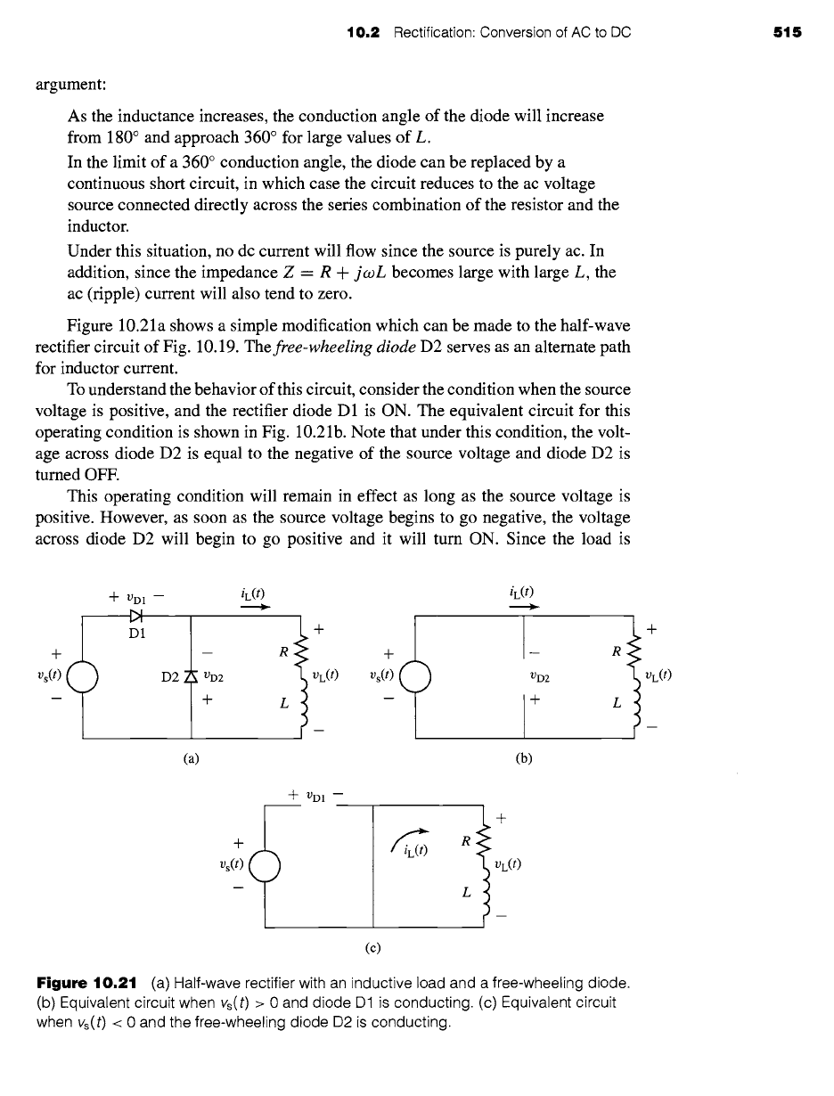
Figure 10.21a shows a simple modification which can be made to the half-wave
rectifier circuit of Fig. 10.19. The
free-wheeling diode
D2 serves as an alternate path
for inductor current.
To understand the behavior of this circuit, consider the condition when the source
voltage is positive, and the rectifier diode D 1 is ON. The equivalent circuit for this
operating condition is shown in Fig. 10.2 lb. Note that under this condition, the volt-
age across diode D2 is equal to the negative of the source voltage and diode D2 is
turned OFE
This operating condition will remain in effect as long as the source voltage is
positive. However, as soon as the source voltage begins to go negative, the voltage
across diode D2 will begin to go positive and it will turn ON. Since the load is
Jr- VD1- iL(I)
D1 +
+
--
R +
Vs(t) D2 VD2 VL(t) Vs(t)
-- + L --
(a)
iL(t)
VD2
+
(b)
+
R
VL(t)
L
+
Vs(t)
q- VD1 --
(c)
+
R
VL(/)
L
Figure 10.21 (a)
Half-wave rectifier with an inductive load and a free-wheeling diode.
(b) Equivalent circuit when Vs(t) > 0 and diode D1 is conducting. (c) Equivalent circuit
when Vs(t) < 0 and the free-wheeling diode D2 is conducting.