Czichos H., Saito T., Smith L.E. (Eds.) Handbook of Metrology and Testing
Подождите немного. Документ загружается.

218 Part B Chemical and Microstructural Analysis
collected by the same objective lens and focused again
but now at an exit slit that is placed at the confocal posi-
tion of the entrance aperture. The light passing through
the confocal aperture is detected by a photosensor. The
light from the sample may be luminescence from a sub-
stance at the focal spot. The important point is that light
from points on the sample other than the focal spot are
rejected by the confocal exit aperture, thereby greatly
reducing stray background light. If we scan the sample
laterally with respect to the objective lens, we obtain
a two-dimensional image on the screen. It should be
pointed out that, although the point resolution is limited
to a subwavelength (a few hundred nanometers) due to
the effect of light diffraction, tiny objects much smaller
than the resolution limit may be viewed as bright spots
when they scatter or emit light visible to the human eye
or detectable by a photosensor. This means that signals
from even a single molecule can be detected if their
separation from other molecules is large enough. A dis-
advantage of LSCM is the long image acquisition time
due to its scanning nature.
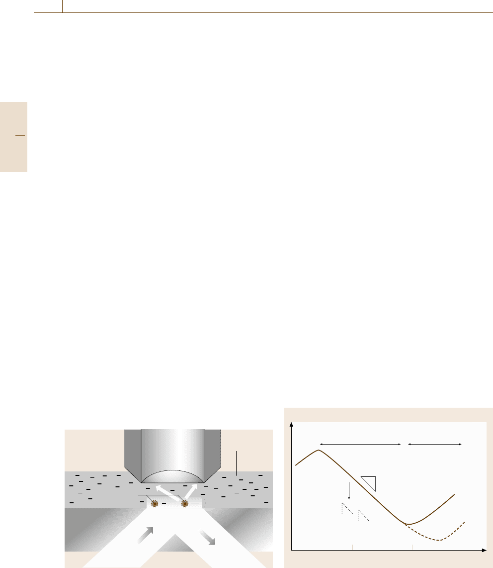
TIRFM is based on the evanescent waves generated
when light is incident onto an interface between two
optical media of different refractive indices. It uses an
ordinary fluorescence microscope equipped with a sam-
ple illumination system, as shown in Fig. 5.11. Samples
attached to the surface of a glass plate are labeled
by fluorescent molecules (fluorochromes). The back of
the glass surface is illuminated with light at an an-
gle smaller than the critical angle for total internal
reflection, so that only fluorochromes within the small
extension distance (< light wavelength) of the evanes-
cent wave are illuminated to induce fluorescence, which
is imaged by the objective lens. The sample may be im-
mersed in a liquid whose refractive index is smaller than
Objective
lens
Water
solution
Fluorescent
molecules
Total reflecting lightIllumination light
Glass
plate
Evanescent wave
Fig. 5.11 The principle of total internal reflection fluores-
cence microscopy
that of glass, so the magnification can be increased up
to ×100 by immersion, and biomolecules can be inves-
tigated in vivo in water solutions. TIRFM is superior to
LSCM in its high speed of image acquisition.
Transmission Electron Microscopy (TEM) [5.14]
Electrons interact so strongly with solids that they
cannot penetrate thick solids. Figure 5.12 shows the de-
pendence of the electronic absorption cross section on
the electron energy. Electrons lose their energy most ef-
ficiently by exciting plasmons in the low energy range
(10–30 eV), but the cross section governed by electronic
excitations decreases with increasing kinetic energy of
electrons except at core excitation edges that are specific
to the elements contained in the sample until it increases
due to the start of Bremsstrahlung radiation loss. There-
fore, if the sample thickness is smaller than ≈ 1 μm,
electrons of energies higher than ≈ 100 keV can pene-
trate the film sample to some extent. A key issue for
TEM studies is how to prepare samples thin enough
for observation. The most common method is chem-
ical thinning by using a chemical etchant after a prior
mechanical thinning process, though a suitable etchant
cannot always be found. The advent of the ion milling
method using an accelerated Ga ion beam for sputtering,
however, has relieved the common difficulty in sample
preparation and so widens the range of materials that
may be studied by TEM.
A great advantage of TEM over other microscopic
techniques is its ability to switch operation between
the imaging and diffraction modes very easily, thereby
investigating in situ the crystallographic properties of
a specific sample area just being observed in the image.
10
3
10
6
1
10
2
smaller
logσ
logE (eV)
Plasmon loss
Bremsstrahlung
radiation loss
Heavy elements
Light elements
Core loss
(ionization loss)
≈ 0.05nm
1
1
L
K
Fig. 5.12 Energy dependence of the absorption cross sec-
tion of electrons
Part B 5.1
Nanoscopic Architecture and Microstructure 5.1 Fundamentals 219
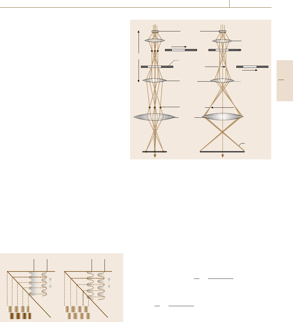
Figure 5.13 illustrates the electron optics of ordinary
TEM in the two modes. Essentially, in the imaging
mode, the image in the real space formed on the im-
age plane of the objective lens is projected onto the
fluorescence screen, whereas in the diffraction mode
the diffraction pattern formed on the back focal plane
is projected onto the screen just by changing the focal
length of the intermediate electromagnetic lens. Usu-
ally, for observations of inhomogeneities in samples, to
obtain an image arising from a specific diffraction an
(objective) aperture is inserted at the back focal plane
where a diffraction pattern is being formed. To ob-
tain a diffraction pattern from a specific area of the
sample, an aperture for selected area diffraction (SAD)
is inserted at the image plane of the objective lens.
Usually the objective aperture selects only the direct
beam, so the images obtained generally look bright
(contrasted against a gray background due to absorp-
tion) with varying contrast due to inhomogeneities, and
are therefore called bright-field (BF) images. Occa-
sionally, a diffracted beam can be selected to brighten
the images of the imperfections responsible for the
diffraction against the dark background, leading to
a dark-field (DF)image.
In most cases, a TEM image is an interference pat-
tern of the electron waves diffracted by a crystalline
sample. Therefore, no correct interpretation of a TEM
image is possible until one carefully compares images
acquired under various diffraction conditions. Although
the quantitatively precise interpretation of TEM images
requires the dynamical theory, the images in many cases
can be understood rather intuitively in the framework of
the kinematical theory. Nevertheless, in some important
cases, dynamical effects or multiple reflection effects
must be taken into account. As illustrated in Fig. 5.14,
a) b)
I
0
I
g
Wedge sample
Direct Diffrac-
ted
Direct Diffrac-
ted
I
0
I
g
s
–1
s
eff
≈ξ
g
–1
Fig. 5.14a,b Periodic exchange of electron energy be-
tween direct and diffracted waves.
(a) kinematical case
|ξ
g
|
−1
|s| and (b) dynamical case |ξ
g
|
−1
|s|≈0. Af-
ter [5.16]
a) b)
Specimen
Remove aperture
SAD aperture
Intermediate
image 1
Variable
focus
length
Fixed
focus
length
Second
intermediate
‘image’
Fixed
Objective lens
Objective
aperture (back
focal plane)
Remove aperture
Intermediate
lens
Projector
lens
Final image
Screen
Diffrac-
tion
pattern
Fig. 5.13a,b Electron optics of transmission electron microscope in
the diffraction mode A and in the imaging mode B. After [5.15,
p. 144]
a beam incident with a Bragg angle of θ
B
onto a set
of net planes is reflected to give rise to a diffraction
beam which may be reflected again by the reverse side
of the same net planes returning to the primary beam di-
rection. If the crystal is thick, this process is repeated
with the electron energy being interchanged periodi-
cally between the direct beam and the diffracted beam.
When only one diffraction g is excited, a detailed analy-
sis [5.16] shows that the intensity of the direct wave and
that of the diffracted wave emanating from a sample of
thickness t are given by
I
0
=cos
2
(πs
eff
t)
+
s
eff
ξ
g
2
−1
πt
ξ
g
2
sin
2
(πs
eff
t)
(
πs
eff
t
)
2
(5.10)
and
I
g
=
πt
ξ
g
2
sin
2
(πs
eff
t)
(πs
eff
t)
2
, (5.11)
respectively, where ξ
g
, the so-called extinction distance
(The terms extinction distance or extinction effects of-
ten used in textbooks originate from the fact that, due to
the diffraction effect, within the distance ξ
g
the primary
beam intensity decays, or is extinguished, more rapidly
Part B 5.1
220 Part B Chemical and Microstructural Analysis
than expected from the energy absorption effect), is de-
fined as
ξ
g
≡
πΩ cos θ
B
λF
g
, (5.12)
where Ω is the volume of the unit cell, θ
B
is the Bragg
angle, λ is the electron wavelength, and F
g
is the struc-
ture factor for g. The parameter s
eff
is
s
eff
≡
s
2
+ξ
−2
g
, (5.13)
where s denotes the deviation from the Bragg condition
in reciprocal space. Figure 5.14 shows schematically
how the two intensities vary with the thickness of
a wedge-shaped sample. When
ξ
g
−1
|
s
|
(Fig. 5.14a)
or t ξ
g
, we could apply the kinematical theory, in
which the thickness dependence is determined by s.
On the other hand, when
ξ
g
−1
|
s
|
≈0(Fig.5.14b)
or t >ξ
g
, the transmission intensity must be treated
rigorously by the dynamical theory, where s
eff
→ ξ
−1
g
and the two beams exchange their intensities, alternat-
ing with a period of ξ
g
, not s
−1
. One should note that
I
0
+I
g
=1 throughout the sample. For its resemblance
to the behavior of two coupled pendulums, this effect
that gives rise to thickness fringes is referred to as
Pendellösung, which forms the basis of similar fringe
contrasts not only in TEM but also in x-ray topography.
In imperfect crystals, the argument is modified by intro-
ducing an additional phase shift due to the presence of
defects. The consequence is described in Sect. 5.3.
The Pendellösung effect embodies the presence of
two dispersion branches at the zone boundary corres-
ponding to the Bragg diffraction at K = g.Itmaybe
regarded as a consequence of beating between the two
Bloch waves on the two branches. They have amplitudes
a)
b)
Branch 1 Branch 2
Atomic columns
Fig. 5.15a,b Bloch waves on two dispersion branches.
Waves
(a) and (b) are absorbed less and more, respectively
at different column positions as shown in Fig. 5.15:
The wave (a) has its amplitude in between the atomic
columns whereas the wave (b) along the columns. Since
the interaction of the waves with the atoms is weak in
(a) but strong in (b), the waves (a) and (b) are absorbed
by the crystal to a lesser and greater extent, respec-
tively. This causes the effects of anomalous absorption
(Kikuchi patterns in electron diffraction, Sect. 5.5.1)
or anomalous transmission (Electron channeling,
Sect. 5.5.1) for electrons and the Borrmann effect for
x-rays, Sect. 5.3.2) propagating in particular directions.
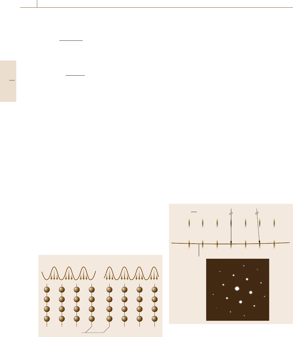
The Ewald sphere in the diffraction of TEM elec-
trons of energy ≈ 100 keV is large compared with the
reciprocal lattice parameter. The reciprocal lattice points
are broadened perpendicular to the sample surface due
to the small thickness of the sample in TEM. As a con-
sequence, if the thickness is smaller than ≈100 nm, the
electron diffractions practically occur in many g vectors,
asshowninFig.5.16. This makes it possible to form
an image by collecting many diffraction beams, includ-
ing those of large
|
g
|
values that contain information
of small-scale structures in the sample. This is the ba-
sis of high-resolution transmission electron microscopy
(HRTEM) which is now a standard installation in mod-
ern TEM microscopes owingto the technological progress
in the improvement of spherical aberration of the objec-
tive lens. Under a special defocusing condition, called
Ewald sphere
k
0
k
|k|=|k
0
|=
2π
λ
Fig. 5.16 Ewald construction of electron diffraction in
TEM. The reciprocal lattice points are elongated normal
to the surface of thin specimens, so that many diffractions
can be excited
Part B 5.1
Nanoscopic Architecture and Microstructure 5.1 Fundamentals 221
a) b)
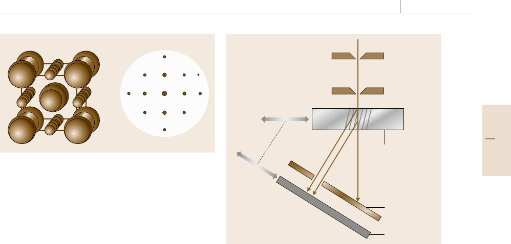
Fig. 5.17a,b The principle of high-resolution TEM. (a)
A perspective view of a schematic crystal along an axis
along which the electron beam is incident to obtain a sym-
metric diffraction pattern, as schematically shown in (b).
Diffracted beams with large wave numbers are collected to
form a high-resolution TEM image that represents, under
the Scherzer defocus condition, approximately the projec-
tion of the atomic columns viewed along the direct beam
the Scherzer defocus, the HRTEM images represent ap-
proximately the arrangement of atomic rows viewed
along the direction of the electron beam, as illustrated in
Fig. 5.17. HRTEM images depend sensitively on the de-
focus condition, the sample thickness, and the depth of
the object in the films. The true atomic arrangements can
be deduced only by careful comparison of experimen-
tal images taken under various defocusing conditions
other than the Scherzer defocus and theoretical images
simulated for model structures using the dynamical the-
ory. The routine resolution (point resolution) of HRTEM
is ≈0.2nm.
X-Ray Topography (XRT)
As with transmission electron microscopy, x-ray
diffraction may be used to image crystallographic
inhomogeneities in crystalline samples. A signifcant
difference from TEM, however, is the lack of good
lenses for x-rays so images cannot easily be magnified
as in OM and TEM. The best resolution is determined
by the particle size of the emulsion in x-ray films, typi-
cally around 2–3 μm, which may be reduced to ≈1 μm
by the use of synchrotron radiation. The simplest setup
for x-ray topography (XRT) is one devised by Lang
shown in Fig. 5.18. A version using reflected beams for
imaging (the Berg–Barrett method) is also used, par-
ticularly when the sample is not transparent to x-rays.
XRT images are obtained by recording diffracted beams
of a certain g vector, equivalent to dark-field images
in TEM. An advantage of XRT over TEM is that it
can examine rather bulky samples in a gaseous atmo-
X-ray beam
Translator
Sample crystal
Beam stopper
X-ray film
Fig. 5.18 Lang camera for transmission x-ray topography.
The crystal and the x-ray film are simultaneously trans-
lated to record a topographic image consisting of sample
sections
sphere. Owing to this fact. together with the higher
accuracy in the detection of strains, XRT is suitable for
studies of phenomena in which the stress state is of pri-
mary importance (e.g., fracture). A judicious choice of
diffraction geometry as well as x-ray wavelength and
sample thickness allows high topographic contrast. Ap-
plications of XRT are described in Sect. 5.3.2.
High-Angle Annular Dark-Field STEM
(HAADF-STEM)
In scanning transmission electron microscopy (STEM),
an electron beam focused to a small size is raster
scanned in parallel across a sample surface and a detec-
tor collects some signal arising from the interaction of
the electrons with the sample solid. The signal intensity,
which may vary over the sample position depending on
the crystal structure, orientation, composition, etc., is
used to construct two-dimensional maps of the material
properties in each pixel. The spatial resolution of STEM
is limited by the size of the focused probe beam. The
advantage of STEM is that it does not need imaging
lenses that inevitably have some chromatic aberration
and limit the resolution of TEM images, and the sam-
ple thickness may be relatively thick in comparison with
TEM samples. A demerit of STEM is the lower speed
of image acquisition (seconds to minutes for a single
image) due to the serial recording of the signal.
Part B 5.1
222 Part B Chemical and Microstructural Analysis
In bright-field (BF) STEM, the signal collected is
the directly transmitted electrons that are not diffracted
by the crystallographic sample. Similarly, dark-field
(DF) STEM images can be obtained by collecting only
diffracted electrons. Although the imaging principle of
STEM is different from that of TEM, the two micro-
scopic techniques could be viewed as equivalent if one
regards the electron detector in STEM as the objective
aperture in TEM, both of which are (not physically as
for the detector in STEM) placed at the back focal plane
of the objective lens.
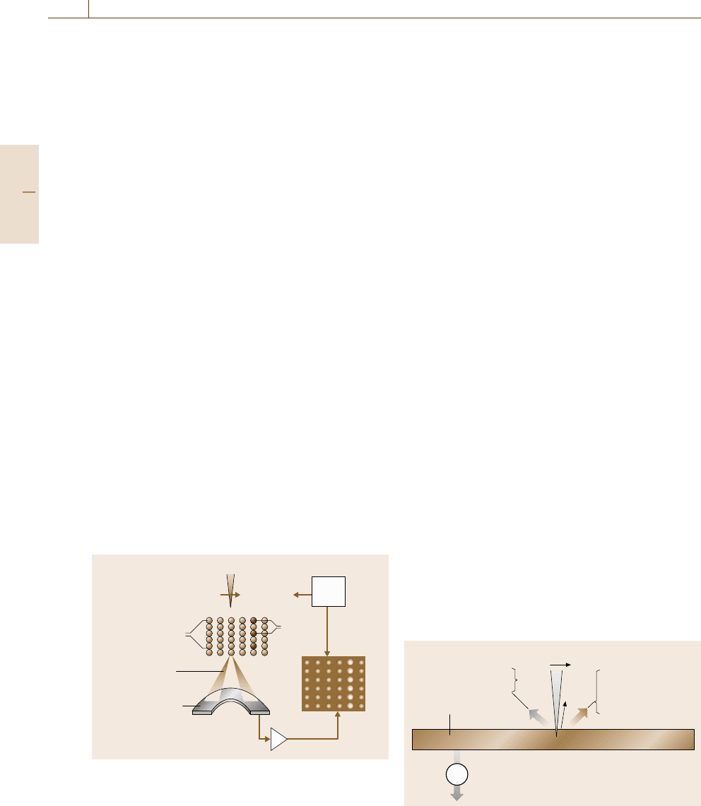
High-angle annular dark-field STEM (HAADF-
STEM) allows one to observe STEM images with
higher resolution and compositional information. As
shown in Fig. 5.19, HAADF-STEM images are formed
by collecting high-angle scattered electrons with an an-
nular dark-field detector placed at the back focal plane
of the objective lens. The image formation mecha-
nism is based on the fact that a fraction of electrons
incident on a crystalline sample along a channeling
direction are diffusely scattered by thermal vibrations
of atoms at relatively high angles ( 70 mrad) when
the beam scans over the atomic columns. Therefore, in
HAADF-STM images, the positions of atoms are ob-
served as bright contrasts depending strongly on the
average atomic number of the atoms in the column.
Owing to this feature, HAADF-STM, otherwise called
Z-contrast imaging, is a powerful technique for compo-
sition analysis especially for elements of large atomic
numbers. The spatial resolution in HAADF-STEM is
limited by the size of the focused probe beam as in or-
Focused electron beam
Convergent angle
≈ 10 mrad
Probe size & 0.2 nm
Beam scan
Scan
circuit
Raster scan
2-D
Map
Small Z
Large Z
Scattering angle
& 70 mrad
Annular detector
Collected current
Fig. 5.19 Setup of high-angle annular dark-field scanning
transmission electron microscopy (HAADF-STEM). Elec-
trons diffusely scattered by thermal vibrations of atoms
with relatively high angles are collected by an annular de-
tector to form a scan image
dinary STEM. Under good conditions, an atomic-level
spatial resolution can be achieved, although such sam-
ples must be thin enough (usually thinner than several
tens of nanometers) for beam broadening to be avoided.
The advantage of HAADF-STM over HRTEM is the in-
sensitivity to focusing conditions and sample thickness
variations, both of which very substantially affect the
phase sensitive contrast of HRTEM images.
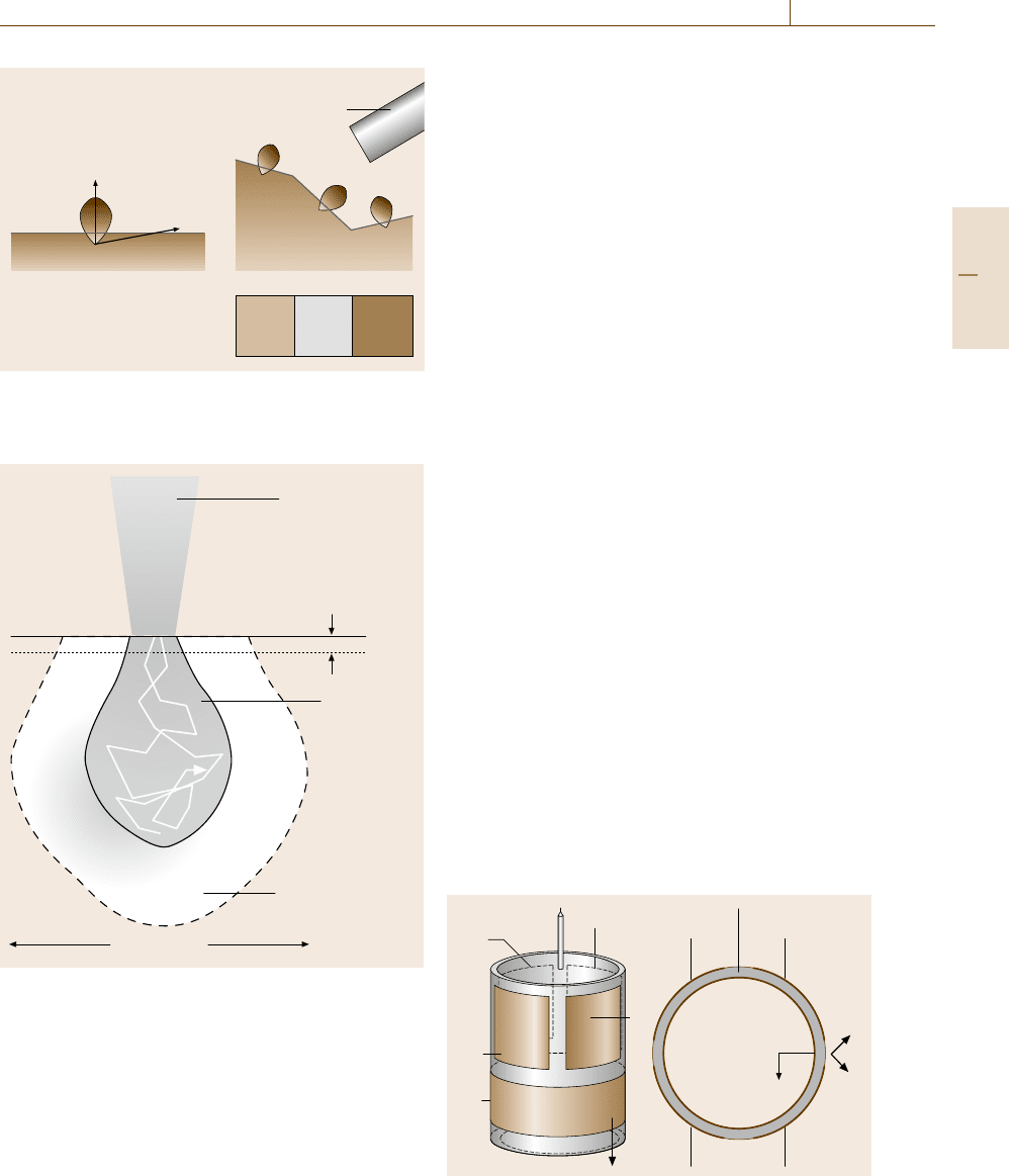
Scanning Electron Microscopy (SEM). The representa-
tive microscope of the scanning type is the scanning
electron microscope (SEM)[5.17], in which the scan-
ning probe is a finely focused electron beam. Fig-
ure 5.20 shows various forms of signals generated by
incidence of electrons onto solid samples. Some of the
incident electrons lose most of their initial energy and
are emitted from the surface with a low energy (≈afew
tens of eV). These electrons are called secondary elec-
trons, which can escape only from very shallow depths
of the solid due to their large absorption cross section
(Fig. 5.12). Without losing much energy, other electrons
are either reflected backward as back-scattered elec-
trons or absorbed into the solid as a drain current. On
the loss of electron energy, x-ray fluorescence or Auger
electron emission occur, which are very useful for elem-
ent analysis. In semiconductor samples, the electron
energy may be converted to a luminescence (cathodo-
luminescence, CL) or an electron-beam-induced current
(EBIC) when an electric field separating electron–hole
pairs is built up in the surface layer. Depending on the
detected signal, SEM has several operation modes. The
most common mode is secondary electron SEM (SEM-
SE), in which the difference in the escape probability of
secondary electrons depending on the direction relative
to the surface normal produces surface roughness con-
trast observed from an oblique angle when the electron
detector is placed as shown in Fig. 5.21.
Finely focused beam scan
X-ray fluorescence
Cathodoluminescence
Secondary electrons
Backward scattered
electrons
Auger electrons
Electron beam induced current
A
Sample
Fig. 5.20 Signals generated in scanning electron micro-
scopy
Part B 5.1
Nanoscopic Architecture and Microstructure 5.1 Fundamentals 223
Secondary
electron detector
Fig. 5.21 Escape probability of secondary electrons (SE)
with its maximum in the surface normal direction render-
ing the morphological contrasts in SEM-SE
Electron
probe beam
Escape depth of
secondary electrons
≤1nm
Spread range
of injected
electrons
≥
Generation
range of
secondary
electrons
Diffusion range
of minority carriers
(semiconductors)
≤ a few μm
≤1nm
Fig. 5.22 Factors governing the spatial resolution in SEM
The spatial resolution depends on what signal is
used and how large the signal is. As illustrated in
Fig. 5.22, incident electrons are spread by a random
walk on the nanometer range that increases in depth
with increasing acceleration voltage. For the primary
beam size to dominate the resolution in SEM-SE,we
should choose an accelerating voltage at a medium
value to reduce the lateral spreading of electrons. In
commercial SEM-SE operated at 5 keV, subnanometer
resolution is achievable by the use of a field emission
gun, the high brightness of which allows extremely fine
focusing of the probe beam. The resolution in SEM-SE
is determined by the spread range, while the resolution
in SEM-CL and SEM-EBIC is worsened by the dif-
fusion of the carriers generated by the electrons. The
samples for SEM observations must be more or less
electrically conductive to avoid charging effects. If they
are not metals or semiconductors, precoating the sam-
ples with Au films may work.
For samples which are too thin for the fast electrons
to excite secondary electrons for SEM-SE observations,
the use of low-energy electrons (< 1keV)orinactive
light He
+
ions for the probe beam enables studies for
such samples as single-walled carbon nanotubes.
Scanning Probe Microscopy. Since the advent of scan-
ning tunneling microscopy (STM)[5.18–20], the use of
extremely sharp tips controlled by a piezo-actuator as
showninFig.5.23 opened fascinating opportunities to
study materials on the nanometer scale. To date, many
schemes of scanning probe (tip) microscopy (SPM)
have been devised, though some of them are still under
development at present.
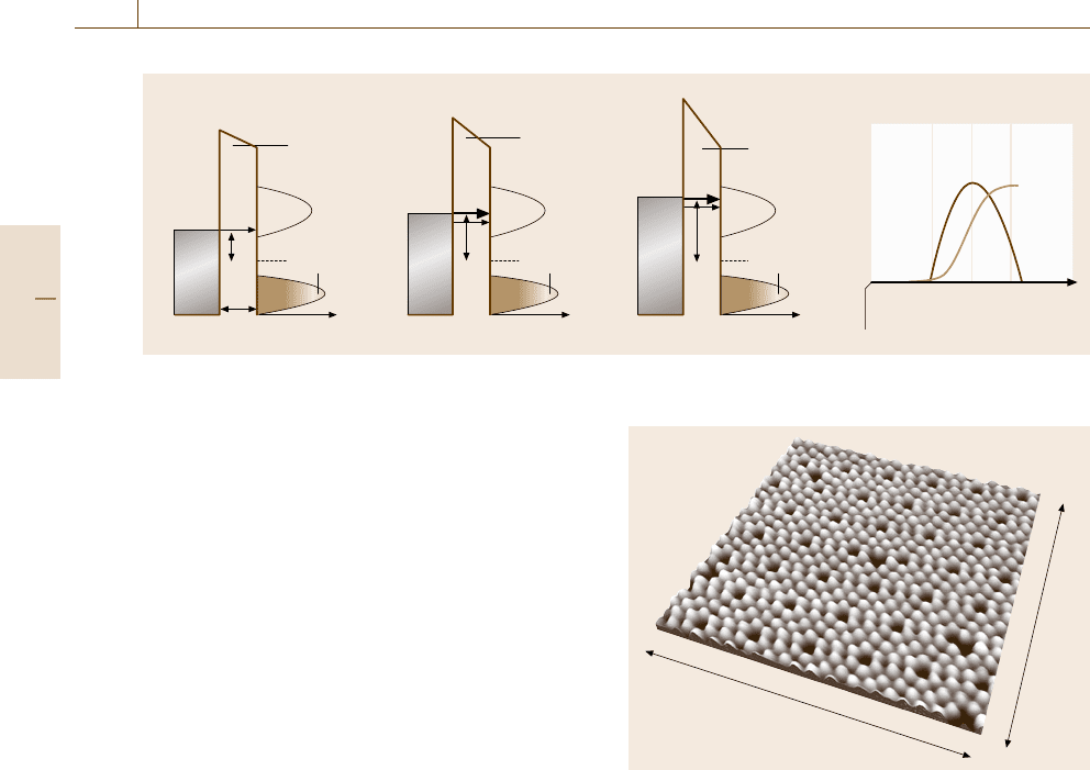
Scanning Tunneling Microscopy (STM). The STM is
based on the fact that a quantum mechanical tunnel-
ing current flows between two electrically conductive
solids closely spaced within a distance of ≈1 nm under
an electric bias voltage, with a very sensitive depen-
dence on the separation. Figure 5.24a–c illustrates the
situation for a combination of metallic tip and a semi-
conductor sample. If the probe tip, usually an electro-
chemically etched tungsten needle, is sharp enough, the
tunneling current is confined to a very narrow region
Tip Piezo-actuator
–V
x
–V
y
+V
y
+V
x
+V
z
–V
x
–V
y
+V
y
+V
x
y
x
Fig. 5.23 Piezo-actuator (tube scanner) for tip scanning
Part B 5.1
224 Part B Chemical and Microstructural Analysis
a) b) c) d)
a) b) c)
E
F
(Tip)
E
F
(Sample)
LDOS
Metal tip
Vacuum
gap
Sample
E
F
(Tip)
E
F
(Sample)
LDOS
Vacuum
gap
Sample
V
b
z
V
b
E
F
(Tip)
E
F
(Sample)
LDOS
Vacuum
gap
Sample
V
b
V
b
Metal tip Metal tip
E
F
(Sample)
V
b
dI
t
/dV
b
I
t
LDOS
Fig. 5.24a–d Vacuum tunneling between a metallic tip and a semiconducting sample, also illustrating the principle of
scanning tunneling spectroscopy
(< 0.1 nm) beneath the tip. Scanning a sample surface
with such a sharp tip and recording as a signal the volt-
age applied to the piezo-actuator that acts to keep the
tip–sample distance (more precisely the tunneling cur-
rent) constant, we can obtain a two-dimensional image
of the surface topography, as shown in Fig. 5.25.
STM images generally reflect very strongly the lo-
cal density of states (LDOS) of surface electrons on
which the tunneling current is also dependent. This fact
provides a unique method, scanning tunneling spec-
troscopy (STS), for the assessment of local electronic
properties of the samples. Figure 5.24 illustrates the
principle of STS, which is based on the fact that most of
the external bias voltage is applied across the vacuum
gap and that electron tunneling occurs from electronic
filled states to empty states conserving energy. The tun-
neling current I
t
varies with the bias voltage V
b
as in
Fig. 5.24d with its derivative with respect to V
b
approx-
imately representing the LDOS.
In principle, STM experiments could be conducted
in ambient environments as long as the current is con-
fined beneath the tip, but in most cases clean surfaces
are investigated in ultra-high vacuum to obtain re-
producible results. Preferably, the surface should be
atomically flat with steps in atomic heights; otherwise
in rough surfaces, the tip shape is convoluted with the
image giving a spurious surface morphology.
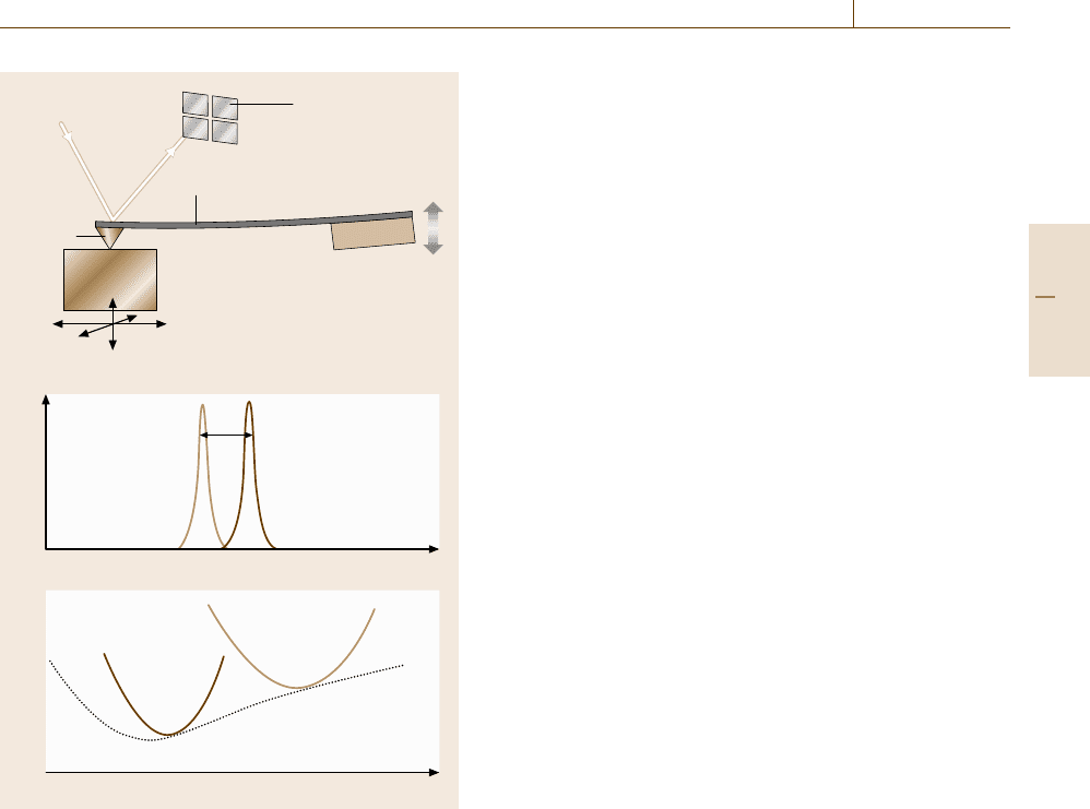
Atomic Force Microscopy (AFM). Atomic force micro-
scopy (AFM) uses a sharp probe tip mounted on
a cantilever, as shown in Fig. 5.26 [5.21, 22]. When the
sample and the tip are close enough, the sample exerts
a short-range force on the cantilever, an attractive force
originating from the van der Waals interaction, a re-
pulsive force due to the Pauli exclusion principle, and
a variable force of chemical origin. The force may also
15nm
18nm
Fig. 5.25 STM image of Si(111)–7 × 7 surface
be long-ranged, arising from a Coulombic interaction.
The simplest AFM with the tip in mechanical contact
with the sample surface detects a force-induced devia-
tion of the cantilever by an optical or electronic method.
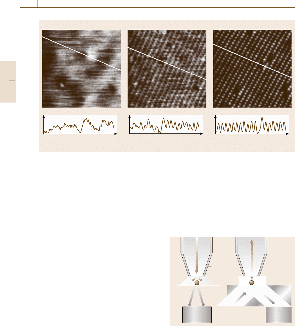
Recently, noncontact AFM has made great progress in
imaging solid surfaces at atomic resolution comparable
with STM. The common technique used for the de-
tection of atomic force is to measure the shift of the
resonance frequency of the cantilever that is caused by
a nonlinear force operating between the sample and
the tip (Fig. 5.26). In the current state-of-the-art instru-
ments, the lateral and vertical resolutions are 10 pm
and one to several pm, respectively. Figure 5.27 shows
a set of noncontact AFM images of a GaAs surface.
An atomic resolution is achieved when the closest dis-
tance z between the sample and the cantilever tip is
shorter than ≈ 0.1 nm (b and c). The blurred contrast
in (a), obtained at a slighty large closest approach, is
considered to indicate the presence of charged defects
beneath the sample surface.
Part B 5.1
Nanoscopic Architecture and Microstructure 5.1 Fundamentals 225
a)
b)
c)
X-Y-Z
Piezo-actuator
Laser beam
Position-sensitive
detector
Cantilever
Probe tip
Sample
Oscillation amplitude
Oscillation frequency
Frequency shift
2
Tip–sample distance
Tip–sample
interaction
2
1
Potential felt
by the cantilever
1
Fig. 5.26a–c The principle of noncontact atomic force mi-
croscopy (AFM). (a) The sample exerts a force on the
probe tip on top of a cantilever whose deflection is de-
tected, in this case, by an optical lever method. The
cantilever is forced to oscillate at the resonance frequency
(b) which changes with the tip–sample distance due to the
nonlinear interaction between the tip and the sample (c)
Scanning Near-Field Optical Microscopy (SNOM).
Scanning near-field optical microscopy (SNOM)[5.23]
overcomes the diffraction-imposed resolution limit of
OM by exploiting an evanescent field that is gener-
ated and/or detected by a probe tip that is brought
very close to the sample. Usually, the tip is made of
metal-coated optical fiber with a tiny aperture at the
apex. The tip–sample distance may be controlled by
the same technique used in STM and AFM. There are
many SNOM schemes, only two of which are illus-
trated in Fig. 5.28.InFig.5.28a, the light guided by an
optical fiber illuminates the sample in a region that is
highly localized by the aperture, and the light scattered
or emitted by the object is collected by the probe itself
or detected as a far-field light by a photosensor. In the
setup in Fig. 5.28b, the sample on an optically flat glass
is illuminated with an evanescent wave of a total inter-
nal reflecting light. The probe collects secondary light,
or a photodetector senses a change to the total reflected
light intensity caused by the presence of the tip in close
vicinity to the object. More recently, attempts at aper-
tureless SNOM using a metallic tip illuminated with
a macroscopic light to exploit the metal–tip-enhanced
optical field have been reported. In any case, the spatial
resolution at present is limited to tens of nanometers.
SNOM is a rapidly growing technique because of the
wide applicability to materials, regardless of sample
properties such as electrical conductivity, and the flexi-
ble test environments. Interested readers should refer to
most contemporary articles for the latest progress.
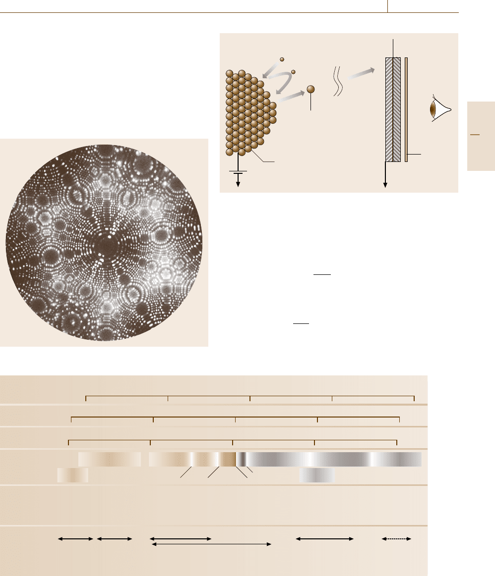
Field Ion Microscopy (FIM). The field ion microscope
(FIM)[5.24] is a type of microscope based on a prin-
ciple completely different from those described so far.
In the basic setup, illustrated in Fig. 5.29, the sample is
a metallic needle the apex of which is atomically sharp-
ened with an end radius of 50–100 nm so that an electric
field applied to the sample is concentrated on the atomic
step edges. The sample faces a phosphor screen placed
at a distance of ≈ 5 cm from the needle tip. To ob-
tain images, a small amount (≈ 10
−3
Pa) of an inert
gas, usually helium, is introduced into the ultra-high-
vacuum chamber in which the sample and the screen
are accommodated, and a positive (with respect to the
screen) bias voltage is then applied to the sample. The
inert gas atoms polarized by the electric field are elec-
trostatically attracted to the tip and migrate further to
the step edges where a high electric field is concen-
trated. When the bias voltage is high enough (a few
tens of V/nm), an electron in the inert gas atom tun-
nels quantum mechanically to the tip resulting in the
formation of a positively charged ion at the step edges.
The ion formed is immediately repelled by the strong
electric field present between the sample and the screen,
and starts to be accelerated towards the screen along the
direction of the electric field. Since the electric field em-
anates radially from the tip apex, the distribution of the
ion impinging spots on the screen, as shown in Fig. 5.30,
represents a highly magnified image of the atoms at the
step edges on the sample tip. Usually, a multichannel
plate is placed in front of the phosphor screen for sig-
nal enhancement. The sample may be cooled to a low
temperature to suppress thermal atomic motion on the
Part B 5.1
226 Part B Chemical and Microstructural Analysis
11.5 nm 11.5 nm 11.5 nm
12.2 Hz
c)b)a)
4.57 Hz1.9 Hz
z ~ 0.4 nm
Δ Δ Δv = –31Hz
z ~ 0.10 nm
v = –62Hz
z ~ 0.08 nm
v = –70Hz
Fig. 5.27a–c Noncontact AFM images of a p-GaAs(110) surface. z denotes the closest distance between the sample and
the tip, and Δν the shift of the cantilever resonance frequency. p-GaAs(110) N
A
=1.4×10
19
cm
−3
(after [5.25])
surface. FIM is useful for three-dimensional microanal-
ysis of element distribution if combined with an atom
probe method (Sect. 5.5.3).
5.1.3 Spectroscopy
Optical Spectroscopy
The physical property of primary importance in optical
spectroscopy is the energy of the photons. Figure 5.31
summarizes the main optical spectroscopic methods ar-
ranged according to the range of photon energies, and
the corresponding wavelengths and frequencies. Al-
though electromagnetic waves in general range from
radio frequency (RF)wavestoγ -rays, we first con-
fine ourselves in traditional optical spectroscopy, which
is usually limited to a range from infrared to ultra-
violet light (It should be noted that, owing to the
development of more intense light sources and more
sensitive light detectors, the techniques now mostly
applied to this range are being extended, based on es-
sentially the same principle, to regions down to THz
waves and up to x-rays. For recent development in
the range of extreme violet (30–250 eV) to soft x-rays
(250 eV–several keV) see [5.26]). The interaction of
light in this range of photon energies with matter
has different origins depending on which quasiparti-
cles (quanta) are excited: electronic, vibrational, or
both coupled (vibronic). In the bottom of Fig. 5.31,
the quanta that can be studied are shown. In this
section, we touch only on matters relevant to this
chapter.
Infrared Absorption Spectroscopy (IRAS)
Fourier transform (FT) spectroscopy has advantages
over spectroscopic measurements using a dispersive
Optical fiber
Photo-
detector
Photo-
detector
Metal
coat
a) b)
Fig. 5.28a,b Two representative setups of scanning near-
field optical microscopy (SNOM) using evanescent waves
(a) from an optical fiber tip and (b) from the surface of
a glass plate internally total reflecting light
Part B 5.1
Nanoscopic Architecture and Microstructure 5.1 Fundamentals 227
monochromator (e.g., a grating monochromator), in
which spectral signals are detected sequentially with
a single detector, under certain conditions. For FT mea-
surements we use, instead of a dispersive monochroma-
tor, an interferometer such as a Michelson-type device
shown in Fig. 5.32. The output of the interferometer
fed with light of wavelength λ and intensity I
0
λ
is vari-
able depending on Δx, the displacement of the movable
Fig. 5.30 FIM Image of a W tip (Courtesy of Dr. K. Hono)
Frequency
Wavelength
Photon
Energy
Spectroscopic
methods
Quanta
studied
1GHz 1THz 1PHz 1EHz 1ZHz
1m 1mm 1μm 1nm 1pm
1μeV 1 meV 1eV 1keV 1MeV
RF
Microwave Far-IR
Visible Soft x-rays
UV hard x-rays γ-rays
NMR ESR FT-IR
IRAS
Absorption
Reflection
PL
Raman
Absorption
UPS
XAFS
XPS
PAC
MB
PAS
Nuclear spin Electronic spin
Rotation phonon
Valence electron
Core electron
Valence electron
core electron
nuclear spin
Near-IRInfrared
Fig. 5.31 The energy of photons used for optical spectroscopic measurements of various quanta
Imaging gas Multichannel plate
Phosphor
screen
Ionized atom
He
He
+
M
+
Sample tip
Fig. 5.29 The principle of field ion microscopy (FIM). Inert imag-
ing gas atoms arriving at the field-concentrated atoms at step edges
are ionized and repelled towards a phosphor screen to project the
atomic image at high resolution
mirror, through
I
λ
(Δx) = I
0
λ
sin
2π
2Δx
λ
. (5.14)
If the movable mirror is displaced at a constant ve-
locity v,thenΔx = vt at time t, and hence
I
λ
(t) = I
0
λ
sin
4πv
λ
t
= I
0
λ
sin
(
ω
λ
t
)
. (5.15)
Equation (5.15) indicates that light of intensity I
0
λ
is sinusoidally modulated at a frequency given by
Part B 5.1
