Venables J. Introduction to Surface and Thin Film Processes
Подождите немного. Документ загружается.

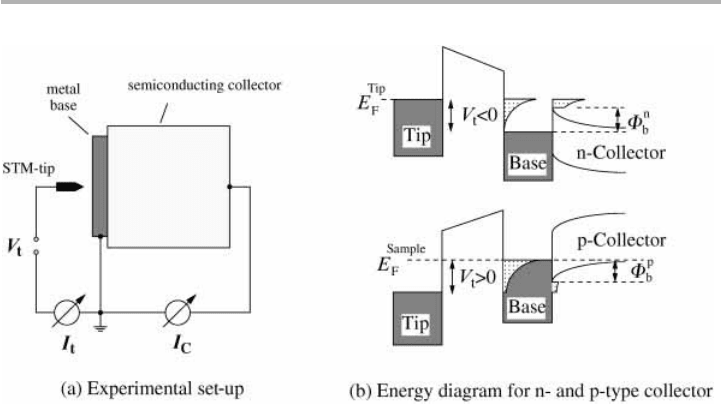
arrangement is shown in figure 8.6. BEEM can be understood as a hot electron triode,
in which the tunneling current (I
t
) into the metal serves as the source for the collected
current (I
c
) in the semiconductor. BEEM images can then be obtained by scanning the
tip, and compared with STM images of the same area, as shown for a thin metallic
CoSi
2
layer on Si(111) by von Känel et al. (1995). The application of STM and BEEM
to study silicides is reviewed by Bennett & von Känel (1999).
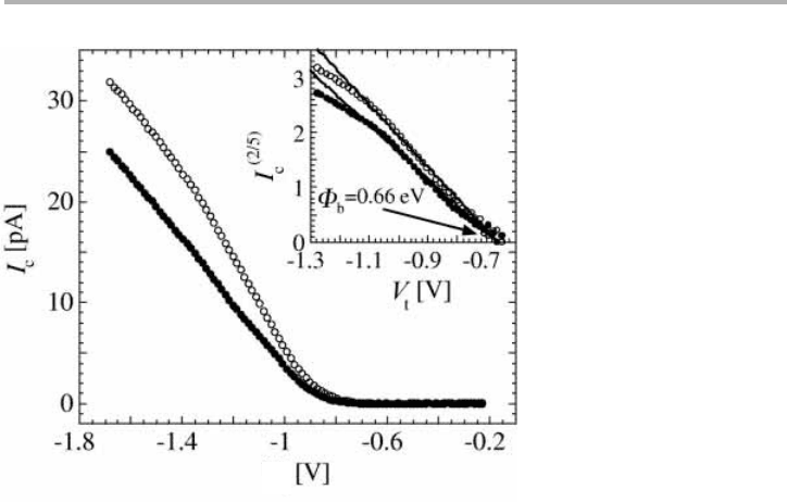
The corresponding spectroscopy (BEES) is possible, also spatially resolved at the
nanometer scale, and has become a very powerful means of determining local values
of the Schottky barrier height, as indicated in figure 8.7. Here I
c
is plotted against the
tip voltage V
t
for constant I
t
, and goes to zero as 2V
t
approaches
f
B
. These
f
B
values
are at least as good as those produced by large area electrical methods: a quite remark-
able achievement (Meyer & von Känel (1997).
It is a current research topic to understand the contrast mechanisms in both the
microscopy and spectroscopy. If the metal base electrode is featureless on the lateral
scale of interest, then BEEM contrast is thought to arise largely through effects occur-
ring at the metal–semiconductor interface, though differences in experimental arrange-
ments may have lead to inconsistencies between different groups. It is notable that
transmission through the base layer as a function of thickness offers a direct measure-
ment of the inelastic mean free path (imfp) for low energy electrons, well below the
minimum in the imfp curves discussed earlier in section 3.3.4. For example, Ventrice et
al. (1996) show that for Au films on Si(100) had
l
i
⬃ 13 nm at room temperature and
15 nm at 77 K, for an injected energy of around 1 eV above the Fermi level. It is thus
reasonable to use base electrodes with thickness up to tens of nanometers in these
techniques.
8.1 Metals and oxides in contact with semiconductors 267
Figure 8.6. (a) Schematic set-up of a BEEM experiment, indicating tunneling and collector
currents I
t
and I
c
and the tip voltage V
t
; (b) energy level diagrams for forward BEEM at an
n-type (top) and p-type collector (bottom) (after von Känel et al. 1995, reproduced with
permission).
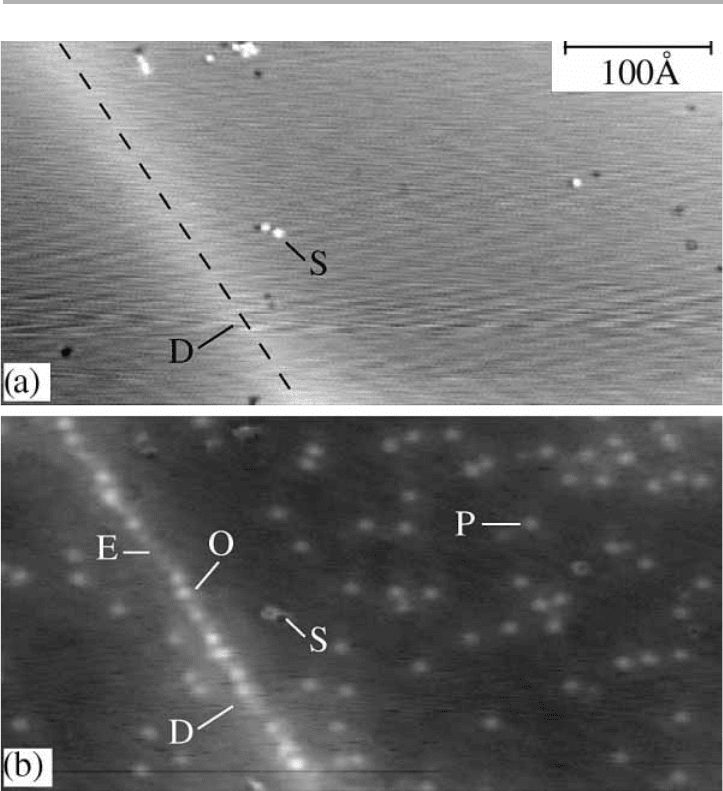
One of the possibilities of BEEM is to identify the defects responsible for surface
states. The images of misfit dislocations in the CoSi
2
/Si(111) interface can be seen at
high resolution to consist of a ‘string of pearls’ as shown in figure 8.8(b), rather than
a continuous line image which one might expect from a dislocation line. In the same
images there are also isolated point defects in the vicinity of the interface, and a sensi-
tivity of below 10
12
cm
22
is claimed (Meyer & von Känel, 1997); the hypothesis is that
it is point defects trapped in the vicinity of dislocations, rather than the dislocations
themselves, which are electrically active.
This sensitivity level is particularly inviting in relation to the SiO
2
/Si and related
interfaces. One of the main reasons why the various MOS and CMOS silicon device
technologies work is the low density of surface states at the Si-SiO
2
interface, where
values below 10
12
cm
22
(i.e. ⬃ 10
23
ML, or 10
10
on 1 mm
2
, or 10
4
on 1 mm
2
), can be con-
sistently achieved. However, it is extremely difficult to deduce what these defects actu-
ally are; the technologist is primarily interested in getting rid of them, and often the
only means of assessing them are the same electrical properties which one is trying to
optimize: a sure recipe for a black art.
Recently, it has been shown that BEEM can address such problems. Using a base
electrode of thin granular Pt, electrons can be injected into, and can be trapped in, a
25 nm thick insulating film of SiO
2
on Si. Trapping of very few (⬃ 10) electrons results
in a decrease of the BEEM current which can then be readily measured (Kaczer et al.
1996). A complementary (broad area) tool is electron spin resonance (ESR), which is
268 8 Surface processes in thin film devices
Figure 8.7. Ballistic electron emission spectra I
c
(V
t
) normalized to the tunneling current, taken
on top of (open circles) or next to (filled circles) an interfacial point defect. I
c
is higher on the
defect for V
t
close to the barrier height
f
B
. The inset shows the 2/5 power of I
c
, yielding a
value of
f
B
50.66 6 0.01 eV (after Meyer & von Känel 1997, reproduced with permisison).
V
t
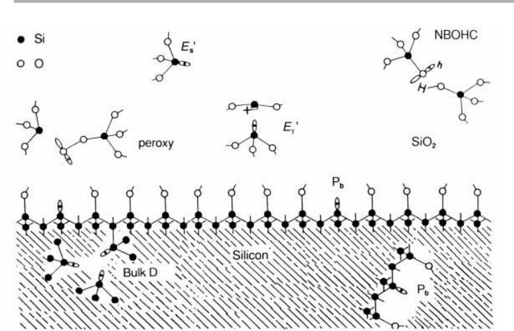
very good for detecting unpaired electrons; these are typically the centers which give
rise to electron traps in SiO
2
, some of which are indicated in figure 8.9. These centers,
for example the P
b
center, which is an electron trapped on a Si dangling bond, are differ-
ent in detail on surfaces of different orientation (Helms & Poindexter, 1994). Another
sensitive wide beam technique is called Total reflection X-ray Fluorescence (TXRF),
which, by using glancing incidence X-rays, can detect below 10
10
(cm
22
) metal atoms on
flat surfaces. It is now highly valued for examining the cleanliness of silicon wafers in
production plant environments (Schroder 1998, section 10.4).
8.1 Metals and oxides in contact with semiconductors 269
Figure 8.8. (a) STM topography image of a 2.8 nm thick CoSi
2
film on Si(111), showing a
0.06 nm high line due to the strain field of an interface dislocation (dashed line);
(b) corresponding BEEM image showing interfacial point defects, S and P, and those trapped
in the core of the interface dislocation D, which comprises empty (E) and occupied (O) regions
(after Meyer & von Känel 1997, reproduced with permisison).
8.2 Semiconductor heterojunctions and devices
8.2.1 Origins of Schottky barrier heights
There has been much discussion of the origin of Schottky barrier heights, and other
related phenomena at metal–semiconductor and semiconductor–semiconductor inter-
faces. As often in physics, there are two limiting cases which can be addressed analyti-
cally, with reality either somewhere in between, or involving other elements not present
in either. The story starts with a half-page paper by Schottky (1938), and continues
with the opposing model of Bardeen (1947). The question to be answered is: what
determines the energy levels in the semiconductor?
In the Schottky model, we bring together the metal and the semiconductor, and
assume there is no electric field in the space between them. This means that we can form
the barrier as the difference between the work function of the metal
f
M
, and the elec-
tron affinity of the semiconductor
x
S
: i.e
f
B
5
f
M
2
x
S
. (8.7)
Equation (8.7) can be simply tested: pick any semiconductor, deposit a series of metals
on it, and measure the barrier height
f
B
. This should scale directly with the metal work
function
f
M
. The test has been done many times (see e.g. Brillson 1982, Rhoderick &
Williams, 1988 chapter 2, Lüth 1993/5 chapter 8) and the variation with metal work-
function is usually much weaker than this model implies. In the case of Mönch’s work
270 8 Surface processes in thin film devices
Figure 8.9. Paramagnetic point defects which have been observed in SiO
2
/Si structures by
electron spin resonance. The NBOHC configuration is the non-bridging-oxygen hole center
(after Helms & Poindexter 1994, reproduced with permission).

on Si(111)231 cited by Lüth, changing metals to give
f
M
varying from 2 to 5.5 eV
increases
f
B
modestly from 0.3 to 0.9 eV.
The opposite Bardeen model assumes that surface states are sufficient to pin the
Fermi level in the semiconductor, and notes that this energy level is placed at
f
0
above
the valence band edge. The top of the conduction band, which forms the barrier, is at
(E
g
2
f
0
) above the Fermi level; thus
f
B
5E
g
2
f
0
, (8.8)
and the barrier height shouldn’t vary at all with the work function of the metal. This
is also rarely satisfied in experiment, and we must consider that these two models con-
tinue to be discussed because they are simple limiting cases. Once one begins to think
in terms of the detailed mechanisms of what happens when two surfaces are put
together to form the interface, then the basis of both models falls apart. For example,
the two surfaces in vacuum may well be reconstructed, and this reconstruction will
change, and may be eliminated in the resulting metal–semiconductor interface. Also
the interfaces may well react chemically, and/or form a complex microstructure: do
such ‘metallurgical’ effects have no influence on the result?
For many years these types of uncertainty lead to a whole series of tabulations of
data, and empirical models which were all more or less specific to particular systems.
This discussion was often played out at conferences, such as PCSI, Physics and
Chemistry of Semiconductor Interfaces, or ICFSI, International Conference on the
Formation of Semiconductor Interfaces, both still going at number 25 (January 1998,
published in J. Vac. Sci. Tech.) and number 6 (June 1997, published in Applied Surface
Science) respectively. Short of absorbing in detail a historical survey, such as those
written by Brillson (1982, 1992, 1994) or Henisch (1984), and to a lesser extent by
Rhoderick & Williams (1988) or Sutton & Balluffi (1995), the question for the ‘inter-
ested reader’ is: what can one extract of reasonable generality from this field?
The model which has most appeal for me is that introduced in 1965 by Heine, and
developed by Flores & Tejedor (1979) and by Tersoff (1984, 1985, 1986). There is also
an interestingly simple free electron model introduced by Jaros (1988). This topic is
reviewed by Tersoff (1987) in the volume by Capasso & Margaritondo (1987), and by
Mönch (1993, 1994). Termed MIGS, this refers not to a Russian fighter plane, but to
metal-induced gap states: i.e. to states which are present in the band gap of the semi-
conductor, and are populated due to the proximity of the metal. This leads to the result
that the Fermi level is pinned at an energy close to the middle of the gap, a similar result
to the Bardeen model, but for different reasons. It further emphasizes the role of the
‘interface dipole’ and seeks to minimize this quantity. As such this becomes a (more or
less) quantitative statement of the underlying point that nature doesn’t like long range
fields, which I have been stressing from section 1.5 onwards. The bones of this argu-
ment are summarized without attribution in a useful introductory text by Jaros (1989).
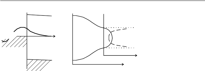
The ingredients of this model can be seen in figure 8.10. We know that there are for-
bidden energy regions in a bulk semiconductor, with an energy gap of width E
g
5
E
C
2E
V
. However, solution of the Schrödinger equation in a periodic potential does
not say that these gap states cannot exist, it merely says that they can’t propagate in an
8.2 Semiconductor heterojunctions and devices 271
infinite medium. Mathematically this means that the k-vector has to have an imaginary
component iq, which ensures decay of the wavefunction; we have seen this as a condi-
tion for a surface state in section 1.5. This decay is slower nearer to the band edges, and
it is most rapid close to mid-gap.
Although this argument does depend in detail on the 3D reciprocal space geometry
of the particular crystal, the 1D model illustrated here, and worked through by Lüth
and by Mönch, gives the essential result. Thus the wavefunctions at these energies
decay into the semiconductor, and must be matched to the traveling-wave solutions in
the metal; this spill-over of charge creates an interface dipole, which is minimized if the
Fermi level is around mid-gap. We have already seen, in section 6.1, that an ML array
of relatively tiny electric dipoles can create quite large changes in electrostatic poten-
tial across the dipole sheet.
8.2.2 Semiconductor heterostructures and band offsets
The above points can be brought out even more forcefully by considering semiconduc-
tor heterostructures, as shown in figure 8.11. We bring together two semiconductors
and ask how the bands will line up. If the semiconductors are similar, but the align-
ment is as in figure 8.11(a), electrons will spill over from right to left; this creates, or is
the result of creating, a substantial interface dipole. However, in the more symmetric
alignment of different semiconductors shown in figure 8.11(b), the electrons in the con-
duction band spill from right to left, whereas the sense is reversed in the valence band.
The resulting charge distribution is much more compensated, i.e. the interface dipole
is a lot smaller, and may even disappear. Simple, that’s the answer!
Considered in terms of the Fermi energy, this problem is rather difficult to pose: we
want the Fermi levels to line up, but at low temperature there are no states at E
F
, so the
problem appears to be undefined. In terms of the interface dipole, however, the
problem appears concrete, even if it is still just a bit elusive. As Tersoff points out, if a
reference level can be found, then the problem is trivial, it has already been solved: this
272 8 Surface processes in thin film devices
Figure 8.10. Elements of the MIGS model: (a) energy levels and wavefunction
c
(z) of states in
the gap close to a metal–semiconductor interface; (b) band diagram including the density of
states (DOS, dashed line) of the MIGS, which peak near the band edges. Note that the length
scale along z in panel (a) is much shorter than the scale d or L in figure 8.4, so that the bands
are shown to be only gently sloping (adapted from Lüth 1993/5).
(a)
E
F
E
V
z()
E
C
z()
ψ( ) ~ ez
–qz
z
(b)
k
iq
E
E
Valence
()
E k
E()
Conduction
k
DOS
C
V

is really what was going on in the Bardeen and Schottky models, but the reference levels
were assumed. Comparable models exist for semiconductor heterostructures. For
example the ionization potential model (often called the electron affinity rule) is the
exact analogue of the Schottky model, where the vacuum potential is the reference
level, whereas the reference level in the case of metals is the Fermi energy. In Tersoff’s
model, the reference point is the branching point energy E
B
, often called the charge
neutrality level, E
n
. It is difficult to pin down the exact definition of this quantity, but
it corresponds to the energy where these states change over (branch) from being valence
band-like to conduction band-like, as in figure 8.10(b), and so usually the energy lies
near to mid-gap.
The electrostatic linear response model presented by Tersoff is instructive, as it shows
why semiconductors are close to the metallic limit. In terms of a polarizability
a
, where
a
5«21, he finds that the valence band offset (VBO) at the interface, DE
V
, is given by
DE
V
5[
a
/(11
a
)]DE
V
n
1[1/(11
a
)]DE
V
0
, (8.9)
where the first quantity DE
V
n
is the difference between the charge neutrality levels, and
the second DE
V
0
is the difference between the ionization energy levels of the materials
in contact. Since for representative semiconductors,
a
⬃ 10, we can see that the first
term on the right hand side of (8.9) dominates, unless DE
V
0
..DE
V
n
. The response (to
the lack of highly accurate ab initio calculations) has often been to make correlations
which are expected to be true if the basic model is on the right track. If metal–semi-
conductor and semiconductor–semiconductor band alignments are similar in origin,
then (E
F
2E
V
) for the metal should parallel (E
B
2E
V
) for the semiconductor, and this
equals the (negative of the) barrier height for a p-type metal-semiconductor contact
f
BP
, since the relevant acceptor states are close to E
V
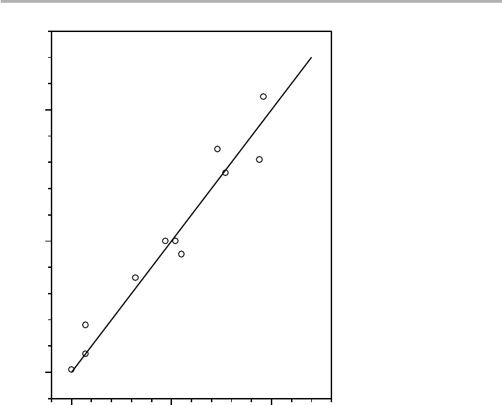
. This correlation, shown in figure
8.12, is perhaps the most successful prediction of the MIGS model.
The challenge for quantum mechanical calculations is that barrier heights and band
offsets are of order 0.3–1.0 eV, and can be measured to 6 0.02 eV precision. As can be
seen in figure 8.12 and in table 8.1, predictions in the late 1980s were good to
⬃ 60.1–0.15 eV. Some calculations have improved to a secure 6 0.1 eV, but claims to
be much better are suspect. In particular, it is not easy to ensure that charge neutrality
8.2 Semiconductor heterojunctions and devices 273
Figure 8.11. Band lineups at semiconductor–semiconductor interfaces, which result in (a) a
strong interface dipole, (b) almost no interface dipole (after Tersoff 1987, redrawn with
permission).
+ + +
+
-
- - -
(a)
+ + +
+
-
- - -
(b)
is maintained across the interface to the required accuracy. One important model of
semiconductor interfaces which builds in this requirement is the ‘model solid’ approach
originated by Van de Walle & Martin (1986, 1987), further developed by Van de Walle
(1989), and reviewed by Franciosi & Van de Walle (1996) and Peressi et al. (1998) as
discussed in the next section.
8.2.3 Opto-electronic devices and ‘band-gap engineering’
Several books (e.g. Butcher et al. 1994, Kelly 1995, Davies 1998) and many conference
articles make it clear that artificially tailored semiconducting heterostructures now
form the leading edge of device technology, and indeed have done so for the past 20
years. By alternating thin layers of, for example, GaAs with (AlGa)As, one can produce
structures with remarkable opto-electronic properties, such as the multiple quantum
well (MQW) laser, and many others. They are fabricated by techniques such as MBE
or MOCVD (see section 2.5) and can be patterned using optical or electron-based
lithography techniques to form real devices (see e.g Kelly 1995, chapters 2 and 3).
274 8 Surface processes in thin film devices
Figure 8.12. Correlation of the p-type Schottky barrier height for Au contacts
f
BP
with the
calculated position of the charge neutrality level (E
B
2E
V
) for several 3–5 and 2–6
semiconductors (after Tersoff 1987, replotted with permission).
0.0 0.5 1.0
0.0
0.5
1.0
Neutrality level
E
B
(eV)
Schottky height,
φ
BP
(eV)
These devices come in various geometries. Many devices use a material structured in
one dimension, perpendicular to the layers, so that the electrons are confined in this
direction and move (freely) in the other direction; this is the basis of the 2D-electron
gas (2DEG) which is used for studying the quantum Hall effect (QHE) and many other
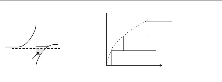
effects. As can be seen in the n-type case illustrated in figure 8.13, the 2DEG exists in
a thin layer where the conduction band of the narrower gap material dips below E
F
;
there are equivalent cases for p-type material. There are also 1D wires (1DEG) and
zero-D dots (0DEG).
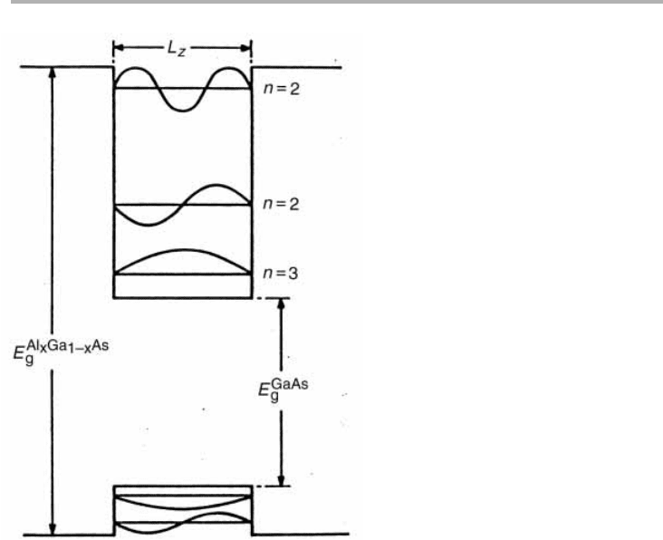
In a QW heterostructure, the electrons and holes are confined in a thin film of the
narrower band gap material, e.g. GaAs, with E
g
51.42 eV at room temperature or
1.52 eV at 0 K, surrounded by an alloy of (AlGa)As, as illustrated in figure 8.14 (the
band gap of AlAs is 2.15 eV at room temperature, see table 8.1). A key quantity is the
valence band offset, DE
V
, or the conduction band offset DE
C
, i.e. (DE
g
2DE
V
). The
energy levels in the well are determined by how the band gap difference DE
g
is parti-
tioned between DE
V
and DE
C
. The quantity Q
C
5DE
C
/DE
g
, the proportion of the gap
difference which appears in the conduction band, is often quoted in data tables, but
DFT and other theoretical models typically give DE
V
with best accuracy.
Although the quantization of the energy levels in the z-direction leads to the 2DEG,
electrons and holes can move in the x and y directions parallel to the interface; so what
is shown in diagrams such as figures 8.13(a) or 8.14 is not a unique level, but the onset
energy of a subband. Within a subband, the 2D density of states is a step function as
shown in figure 8.13(b). For GaAs and similar materials, there are also light and heavy
holes, related to spin-orbit splitting in the valence band, and the material, in contrast
to Si, has a direct band gap. Thus the optical properties of the well are now determined
by the electron and hole masses (three parameters), the well width L
z
,andQ
C
. Duggan
(1987) has given a useful introduction to the determination of optical properties, typ-
ically pursued via optical absorption or photoluminescence (PL) experiments;
another useful starting point is Kelly (1995, chapter 10). As shown in figure 8.15, the
optical absorption (transmission) spectrum shows peaks which can be identified with
light and heavy hole transitions. Note, in passing, that PL experiments only work at
low temperatures, as the transitions are too broad at room temperature, and the
8.2 Semiconductor heterojunctions and devices 275
Figure 8.13. A semiconductor heterostructure giving rise to a 2D-electron gas at zero bias in
n-type material. The energy levels shown in (a) are the onset energies of subbands whose
density of states, N(E), is indicated in (b).
(a)
(b)
E
F
∆E
C
E
C
()z
1st
subband
1st subband
2nd
2nd
3rd
2DEG
NE()
E
3D Envelope ~E
1/2
number of parameters involved causes quite a bit of difficulty for data analysis.
Nevertheless, several parameters can be determined (or assumed in order to get better
values of other parameters), the early work leading to Q
C
values typically in the range
0.6–0.8 for GaAs/AlGaAs heterostructures, and subsequently refined towards the
lower end of this range (Yu et al. 1992, Davies 1998).
In the same volume (Capasso and Margaritondo 1987) there are extensive tabula-
tions of early experimental valence band offsets DE
V
, obtained largely by photoemis-
sion, but also by other techniques including extensions of C–V profiling and DLTS.
Raman scattering has also found a useful niche (Menéndez et al. 1986, Menéndez &
Pinczuk 1988) to measure inter-subband transitions for electrons, and hence DE
C
.
Later compilations and comments are given by Yu et al. (1992), Butcher et al. (1994)
and Franciosi & Van de Walle (1996). Technology moved ahead in the 1990s, e.g. via
the infrared devices based on resonant tunneling via minibands (Capasso & Cho 1994),
but the science had more or less stabilized by the late 1980s. Table 8.1 gives some rep-
resentative DE
V
values for low strain interfaces.
However, it has become clear that pictures such as figures 8.10 and 8.11 are only a
first step, and that too simple pictures may give a misleading impression. Valence band
276 8 Surface processes in thin film devices
Figure 8.14. Simple energy levels in a quantum well, consisting of a narrower band gap
material (GaAs) surrounded by a higher band gap material (Al
x
Ga
12x
As). Note, however, that
the well wavefunctions must in practice spread into the surrounding layers, and the real band
structure modifies this picture (from Duggan 1987, reproduced with permission).
