Venables J. Introduction to Surface and Thin Film Processes
Подождите немного. Документ загружается.


good enough for magnetic field sensors, and read/record heads using GMR multilay-
ers are already commercially available.
In the above example, the nonmagnetic spacer layers (of Cu) were sufficiently thick
to ensure that the magnetism of the Co and NiFe layers are not coupled directly via
the conduction electrons. This is in contrast to the much thinner spacer layers discussed
in section 6.3.4 and illustrated in figure 6.24. At intermediate thicknesses, this spin-
dependent coupling leads to complex magnetization curves, and the transfer of spin
‘information’ from one part of a device to another, which can be used in spin valves or
spin transistors (Parkin et al. 1991, Johnson 1993, 1996, Parkin 1994, Monsma et al.
1995). The next stage may be to make use of spin polarized currents induced by mag-
netic elements into the substrate itself, and then to use these currents as the injector for
a hot electron device (Gregg et al. 1996). The acronym for this UK-based development,
SPICE (spin polarized injection current emitter), may have something to do with the
existence of a popular all-female vocal group of the same name at around the same
time. We shall see what becomes of both.
Another possible way forward, not involving magnetic coupling through the sub-
strate, is to use magnetic wires grown on insulators; these wires have anisotropic mag-
netic properties, as well as being a more favorable geometry for CPP GMR
measurements. NaCl(110) is a substrate with a high surface energy, and self-organizes
into facets on (001) planes at 45° to the substrate plane. By deposition at a shallow
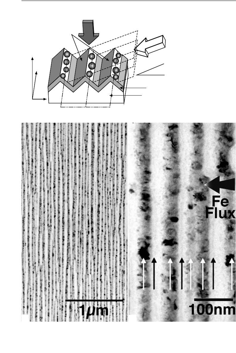
angle, narrow wires will be produced at the tops of the ridges shown in figure 8.18(a),
and these wires can then be capped to prevent oxidation, etc. In a series of experiments,
Sugawara et al. (1997) first deposited a thin SiO layer on either NaCl(110) or (111), fol-
lowed by Fe deposition at a shallow angle, followed by a further SiO layer.
This procedure allowed them to produce isolated islands aligned in one dimension,
continuous parallel wires, or isolated Fe dots of various sizes. They could then remove
the SiO/Fe/SiO assembly by dissolution of the substrate for TEM examination, and to
make particle and wire density observations, exactly as described here in section 5.3, as
shown in figure 8.18(b). The new feature is of course the ability to perform magnetic
and magneto-optical (Kerr) measurements before this stage, similar to that shown here
in figure 6.18, and hence explore magnetic anisotropy, dipole couplings and the para-
magnetic to ferromagnetic transition as a function of particle size (Sugawara &
Scheinfein 1997). There are a large range of parameters to explore, just within this one
system, if anyone wants to take these results to the next stage of implementation as a
working device.
Another system which clearly shows promise as a magneto-optical device is based
on the nucleation of Co dots on Au(111), at the position of the surface vacancies
which occur at the intersection of the (2331) herringbone reconstruction, first
observed by Voigtländer et al. (1991) and described here in section 5.5.3. A strong
Kerr effect signal from ML deposits in these dots has been observed by Takashita et
al. (1996), and Fruchart et al. (1999) have constructed well ordered Co pillars in
Co/Au (111) multilayers, with improved magnetic properties. Whether or not this
system will end up in a real device is not clear: are we ready to use surface reconstruc-
tions and surface point defects so directly in a manufacturing process? Whatever the
8.3 Conduction processes in thin film devices 287

288 8 Surface processes in thin film devices
Figure 8.18. (a) Shadow deposition at glancing angle onto ridged substrates to produce Fe
dots and, at higher coverage, nanowires; TEM pictures at lower (b) and higher (c)
magnification, showing the length and width of the Fe wires in the SiO/Fe/SiO assembly (from
Sugawara et al. 1997, reproduced with permission).
(100)
(010)
NaCl (110)
substrate
[110]
[001]
[110]
a-SiO
SiO deposition
20º
Fe flux
Fe dots
(a)
(b)
(c)

answer, these surface processes can be responsible for observed structures with lateral
length scales in the 10 nm range.
8.4 Chemical routes to manufacturing
Although this book, including this chapter, has been written largely from the perspec-
tive of materials physics, materials-oriented chemistry plays an enormous role in device
development. Chemists are also being drawn into the field of combinatorial materials
discovery, a practically based mix of combinatorial chemistry and thin film deposition
techniques, used to search for new compounds and compositions. Such developments
are discussed briefly in this section.
8.4.1 Synthetic chemistry and manufacturing: the case of Si–Ge–C
The growth of Ge and SiGe alloys on Si(001) was considered in some detail in section
7.3.3. It is the simplest example of strained layer growth, and we described how the low
mismatch alloys can be grown as layers suitable for heterostructures, or the strain can
induce islands to form, which may (or may not) have potential as quantum dots. But
do we want islands, or would layers be better? The answer, of course, depends on the
application envisaged, but in general layers are preferable. So let’s try mixing in another
element, which relieves the strain and so promotes layer growth. This is the motivation
behind research on the Si–Ge–C system; by mixing in the right amount of carbon one
can hope to compensate for the strain introduced by Ge.
But how to do it? CVD is the most widely used manufacturing technique, starting
from silane (SiH
4
) and germane (GeH
4
), so mix in some methane (CH
4
) and see what
happens. But some knowledge of thermochemistry is required, and this tells us that
methane is much more stable than both silane and than germane, which means that
CH
4
does not want to break up. Moreover, the solubility of C in Si or Ge is very low
(⬃ 1310
26
% in equilibrium at the Si melting point, and even lower in Ge), so the
carbon which does form is likely to be in the form of SiC, which is not what we want;
in practice up to 1–2% has been incorporated at SiGe CVD process temperatures
⬃ 700 °C. Somehow we have to trick the system, thermodynamically and kinetically.
This has been done by creating custom-built molecular precursors to use as the source
material.
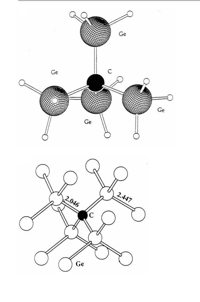
One group in Arizona (Kouvetakis et al. 1998a) has been developing compounds
with an inbuilt tetrahedral arrangement involving one C atom surrounded by four SiH
3
or GeH
3
ligands, as illustrated in figure 8.19(a). These are sizable van der Waals mole-
cules, which are liquids at room temperature and evaporate easily. They are also reac-
tive, in that they lose hydrogen easily, and hence can incorporate the tetrahedral units
Si
4
C and Ge
4
C into a growing film.
These molecules are crowded, and have bond lengths very different from normal, as
indicated in the cluster calculation for Ge
n
C shown in figure 8.19(b). This is because
the small C atom is in the middle, and the much larger Si and especially Ge atoms are
8.4 Chemical routes to manufacturing 289

290 8 Surface processes in thin film devices
Figure 8.19. (a) The precursor molecule (GeH
3
)
3
C, with Ge–C and other bond lengths
determined by gas phase electron diffraction; (b) structure of substitutional C in Ge and the
associated Ge–C and Ge–Ge bond lengths in a calculated (Ge)
n
C cluster (after Kouvetakis et
al. 1998a,b, reproduced with permission).
(a)
(b)

competing for space around it. However, this processing route suppresses the segrega-
tion of the C atoms, because they are always surrounded by Si or Ge, and Kouvetakis
et al. (1998b) have been successful in incorporating 5–6%C into films grown at 470°C,
which have relatively few defects (and no SiC precipitates) as seen by TEM. Starting
molecules with carbon on the outside would not be nearly as effective in this respect;
in other words, by using these special molecules and relatively low processing temper-
atures, carbon has been tricked to remain in solution.
Whether this work represents a real breakthrough or just a very interesting develop-
ment depends on the next stage – will the clever molecules be incorporated into actual
manufacturing processes or not? The role of relatively small contract research firms in
smoothing the path to manufacturing is interesting; such processes will certainly not
be incorporated into large scale Fab lines overnight. Increasingly, it is the equipment
manufacturers who incorporate new processes such as this one, in order to be able to
persuade the large scale producer (of e.g. computer chips) to adopt such technologies
when they reinvest the next few US$ billion.
3
8.4.2 Chemical routes to opto-electronics and/or nano-magnetics
Optoelectronics, the integration of light sensitive devices with micro-electronics, is
another huge field in which surfaces and thin films play a major role. One of the main
interests in the growth of III–V and II–VI compounds is related to the ability to inte-
grate such devices with silicon in the form of ‘band gap engineering’ as discussed in
sections 7.3.4 and 8.2.3. Quantum dots are a hot topic touched on in section 8.2.4,
where the intent is that uniform size and spacing can be achieved via self-organization.
But, as always in technology, one has always to bear in mind that the most effective
solution to the original challenge or problem, might come from a completely different
route. One such possibility is the assembly and self-organization of ordered arrays of
colloidal particles prepared by more or less traditional wet chemistry methods – a flask
full of goo, a drying oven and a spray-gun may be all that is needed; I exaggerate, of
course, but not by much. Such techniques are not specific to optoelectronics; magnetic
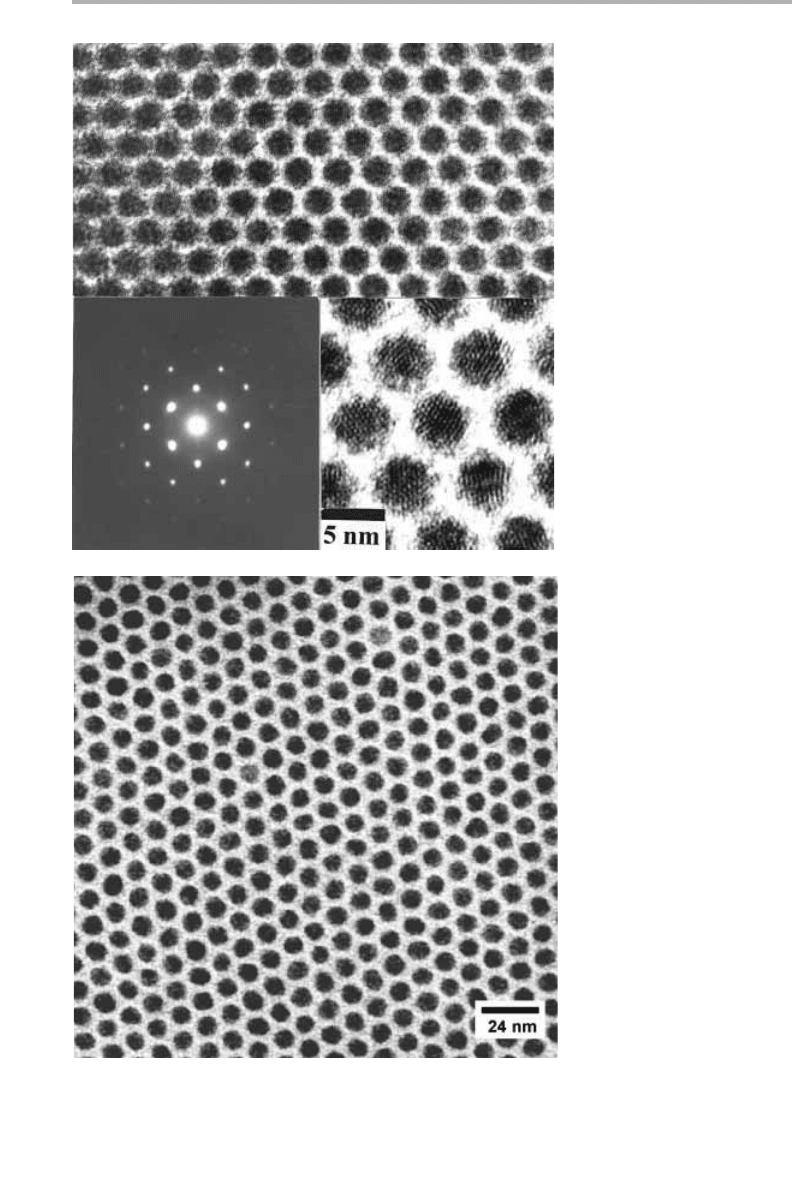
particles can just as well be prepared and arranged in remarkably uniform arrays, as
shown in figure 8.20.
Here the idea is to prepare II–VI materials such as CdSe in solutions containing
additives which adsorb on the surface of colloidal crystals in the size range 5–10 nm,
thus preventing further growth. These colloids, coated with self-assembled monolayers
(SAMs), form a stable dispersion in solution, which can be made to crystallize out by
gentle evaporation of the lighter component in the solution (e.g. octane from octanol
at 80 °C). Further warming removes all but a few ML of the additives, to the extent that
3D colloidal superlattice crystals can be grown with sizes up to 50 mm (Murray et al.
1995, Heath 1995, Collier et al. 1998).
The size distribution is amazingly narrow, as shown in figure 8.20, and can be further
controlled by manipulation of the supersaturation as a function of time during growth.
8.4 Chemical routes to manufacturing 291
3
Financiers should note that the US billion is used here which is only 10
9
, rather than the UK 10
12
.

292 8 Surface processes in thin film devices
Figure 8.20. (a) 3D Optical superlattice formed from colloidal crystals of CdSe, spacing
6.5 nm, diameter 5 nm (similar to Murray et al. 1995); (b) 2D magnetic superlattice of Ag
coated Co particles, spacing 13 nm, diameter 8 nm formed by colloidal techniques (after
Murray 1999, both figures reproduced with permission). In both these cases the 2D hexagonal
lattice extends over much larger distances than can be effectively portrayed here.
(a)
(b)

Other clever tricks are to cap these dots with a compatible material such as CdS having
a higher refractive index or to introduce relevant dye sensitizers onto the surface of the
dots. This latter technique has been a key ingredient in the color photographic pro-
cesses using AgBr crystals for a long time. By the former means the confinement of the
exciton wavefunction can be increased, and so produce stronger photoluminescence,
quantum yields .50% having been demonstrated (Peng et al. 1997, Schlamp et al.
1997). However, until now the overall electro-luminescent energy efficiency has been
low, and the devices are not yet stable enough for production (Peng et al. 1997,
Alivisatos 1998, Collier et al. 1998).
A single electron transistor which functions at T54.2 K has been demonstrated,
simply by sprinkling individual colloidal dots of CdSe across the gate region of an FET
(Klein et al. 1997). As a way forward, you might take this demonstration ‘with a pinch
of salt’, but it is certainly spectacular. One of the arguments in favor of these colloidal
crystals is their intrinsic cheapness, yet if there is no way of getting current in or out,
or if they only work at low temperature, then we have just an intriguing demonstration,
not yet an innovation. Another impressive demonstration is an FET which works at
room temperature, made by dropping a single carbon nanotube across the source-drain
gap (Tans et al. 1998a), and the observation of associated Coulomb blockade phenom-
ena (Tans et al. 1998b).
8.4.3 Nanotubes and the future of flat panel TV
A further example centers around chemical routes to the production of field emission
sources for computer or TV screens. As discussed in section 6.2.2, various carbides and
nitrides have been researched over the years, but have never really been quite stable
enough to make a serious impression on the market. Yet the conventional TV tube is
the last remaining example of the vacuum triode in production; is it too destined for
oblivion? If field emission could be made to work reliably in the planar geometry
shown in figure 6.13(b), then maybe it could be saved!
These thoughts have gained impetus from the discovery of both multiple and single-
walled carbon nanotubes, cylindrical intermediates between planar graphite and the
closed cage fullerenes (Iijima 1991, Ebbesen & Ajayan 1992, Ajayan & Ebbesen 1997,
Bernholc et al. 1997). The tubes grow as long filaments sticking out from the substrate,
and emit electrons from the ends. Filaments can be produced in bundles or matrix
arrays (Collins & Zettl 1997), which differ in detail depending on the production
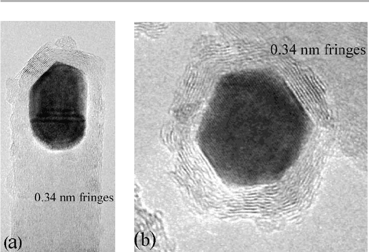
method. Using a plasma arc discharge, Terrones et al. (1998) have produced filaments
containing a transition metal carbide particle near the end. The carbide particle cata-
lytically converts C-containing compounds into tubes, almost as if it were knitting a
sock, as shown in figure 8.21. Several different refractory carbides have been so encap-
sulated, and progress to date is reviewed by Terrones et al. (1999).
Nanotubes can join up in helical (chiral) as well as cylindrical geometries, p-n junc-
tions along the length have been demonstrated where the chirality changes, and they
also can be doped, or made, with various B–N–C mixtures. The case of BN has led to
some exquisitely delicate analytical microscopy, combining pictures analogous to
8.4 Chemical routes to manufacturing 293

figure 8.21 with compositional analysis via EELS on the nanometer scale (Golberg et
al. 1996, 1997). With this number of variables to explore, it seems only a matter of time
before practical displays can be devised to rival those already demonstrated for the
Spindt cathode and DLC geometries. But of course that does not mean that such a
display will necessarily be successful in the marketplace, where it has to compete with
all other flat display technologies as discussed earlier in section 6.2.2, and/or find its
own particular niche. The advantage is the high intrinsic brightness, which may make
it suitable for projection onto a large screen; the list of potential disadvantages will dis-
tinguish optimists from pessimists.
Note that in the above two examples the distinction between surfaces, thin films and
molecules has all but disappeared: the molecule is all surface and is the thin film. What
we are seeing here is an important stage in the development of single molecule elec-
tronics. The next stage is again the transition to manufacturing, which may well be a
rocky road, and test to the limit who is serious. As they say on TV: ‘don’t go away’, or
equivalently ‘watch this space’!
8.4.4 Combinatorial materials development and analysis
The combination of step-wise thin film deposition processes with analysis on a micro-
scopic scale is coming to be known as combinatorial materials development. This series
of techniques uses automated deposition and annealing sequences to produce a series
of different compositions, thicknesses and/or doping levels in a matrix pattern of dots
294 8 Surface processes in thin film devices
Figure 8.21. High resolution TEM images of TaC particles in nanotubes where (a) the TaC
particles are encapsulated at tips, and (b) graphite fringes suggest epitaxial growth on the
particles (from Terrones et al. 1998, reproduced with permission).

distributed in x and y.Different patterns can then be set up in several areas on the same
chip, and then analyzed by a microscopic technique to screen for the ‘best’ properties.
Typically, such techniques will be useful when one has to span a large range of param-
eters, and when theoretical models are of limited use. Stepper motors controlling stage
movements and multiple deposition shutters, with a resolution of a few micrometers
are now available more or less routinely (if expensively), which means that many thou-
sands of different samples can be screened in a single experiment.
An example is the search for improved red phosphor materials to be used in flat panel
displays (Danielson et al. 1997). The starting point materials were polycrystalline ternary
or quaternary oxide layers acting as hosts for ‘activator’ rare earth ions such as Eu or Ce.
Some 25000 individual compositions deposited onto a 3-inch wafer were sampled,
leading to a single best composition of Y
0.845
Al
0.070
La
0.060
Eu
0.025
VO
4
. This composition
was found to be as good as the existing commercial phosphors. It is clearly just a ques-
tion of time before superior thin film materials are found using such techniques, which
originated in the pharmaceutical industry as a means of accelerated drug discovery.
The next stage may well be to combine such approaches with patterned substrates,
so that different areas explore different surface treatments or different growth regimes.
A start in this direction, with emphasis on molecular recognition of metal and semi-
conductor nanocrystals, has been made by Vossmeyer et al. (1998), and patterned
arrays of bio-macromolecules have also been demonstrated. Flexible patterned sub-
strates are also being produced via soft lithography, micro-contact printing and related
techniques (Xia & Whitesides 1998). Such approaches involving microarrays of DNA
are centrally involved in the future of the human genome project (DeRisi et al. 1997).
The huge interest in microbiology means that such experiments, including seletively
tagging the colloidal nanoparticles described in the section 8.4.2, are achieving wide-
spread recognition in the materials community (Mirkin et al. 1996, 1999), even if, or
perhaps because, most of the rest of us are very early on the learning curve. But we can
all recognize the implied potential of the field.
All this suggests that we should consider creating patterned nests for microbes, so that
we can then sit back and let them do our work for us. Indeed Richard Feynman was first
with this suggestion in a famous lecture in 1959 entitled ‘There’s plenty of room at the
bottom’, republished as Feynman (1992) in a new Journal of Microelectromechanical
Systems. I’ll bet that H.G. Wells had the basic idea well before that – is there anything
really new? But this is getting dangerously close to futurology, the proper business of
the twenty-first century, not the twentieth. As this chapter is finalized, in December
1999, the decoding of chromosome 22 made headline news, special millennium issues
of the journals arrived, and I started to read articles entitled ‘The Net Century’, etc. A
few words on such topics and the educational/training implications in the short final
chapter, and I’m done. The twenty-first century is essentially yours: good luck!
Further reading for chapter 8
Davies, J.H. (1998) The Physics of Low-dimensional Semiconductors: an Introduction
(Cambridge University Press).
Further reading for chapter 8 295

Jaros, M. (1989) Physics and Applications of Semiconductor Microstructures (Oxford
University Press).
Ferry, D.K. & S.M. Goodnick (1997) Transport in Nanostructures (Cambridge
University Press), chapters 1–4.
Kelly, M.J. (1995) Low-dimensional Semiconductors (Oxford University Press).
Lüth, H. (1993/5) Surfaces and Interfaces of Solid Surfaces (2nd/3rd Edns, Springer)
chapters 7 and 8.
Rossiter, P.L. (1987) The Electrical Resistivity of Metals and Alloys (Cambridge
University Press).
Sutton, A.P. & R.W. Balluffi (1995) Interfaces in Crystalline Materials (Oxford
University Press) chapter 11.
Schroder, D.K. (1998) Semiconductor Material and Device Characterization (John
Wiley).
Sze, S.M. (1981) Physics of Semiconductor Devices (2nd Edn, John Wiley) chapter 5.
Tinkham, M. (1996) Introduction to Superconductivity (2nd Edn, McGraw-Hill).
296 8 Surface processes in thin film devices
