Venables J. Introduction to Surface and Thin Film Processes
Подождите немного. Документ загружается.


Kelly, M.J. (1995) Low-dimensional Semiconductors (Oxford University Press) chapters
1–3.
Liu, W.K. & M.B. Santos (Eds.) (1999) Thin Films: Heteroepitaxial Systems (World
Scientific).
Lüth, H. (1993/5) Surfaces and Interfaces of Solid Surfaces (2nd/3rd Edn, Springer)
chapter 6.
Mönch, W. (1993) Semiconductor Surfaces and Interfaces (Springer) chapters 7–18.
Pettifor, D.G. (1995) Bonding and Structure of Molecules and Solids (Oxford University
Press) chapters 3 and 7.
Sutton, A.P. (1994) Electronic Structure of Materials (Oxford University Press) chap-
ters 6 and 11.
Sutton, A.P. & R.W. Balluffi (1995) Interfaces in Crystalline Materials (Oxford
University Press) chapter 3.
Tsao, J.Y. (1993) Materials Fundamentals of Molecular Beam Epitaxy (Academic).
Yu, P.Y. & M. Cardona (1996) Fundamentals of Semiconductors: Physics and Materials
Properties (Springer) chapter 2.
Zangwill, A. (1988) Physics at Surfaces (Cambridge University Press) chapter 4.
Problems and projects for chapter 7
Problem 7.1. Band structures of Si, Ge and GaAs
Look up the calculated band structures of bulk Si, Ge and GaAs, and explain the
meaning of the following terms in relation to these three solids:
(a) the existence of a direct versus an indirect band gap, and the position of the con-
duction band minimum;
(b) spin-orbit splitting and the differences between light and heavy holes;
(c) the removal of degeneracy by stress in compressed thin films, e.g. of Ge on Si(001).
Project 7.2. Band structures in tight binding models
Tight-binding pseudopotential models of tetrahedral semiconductors such as Si or Ge
treat the valence s- and p-electrons as moving in the potential field of the nuclei plus
closed shell electrons. Consult selected references for section 7.1, and show one of more
of the following.
(a) That eight electrons are required to describe the system, resulting in the need to
diagonalize an 838 matrix to solve for the band structure as a function of the wave
vector k.
(b) That a possible approach to this problem is to use sp
3
hybrid states as the basis set,
formed by linear combinations of 1 s- and 3 p-electrons as in equation (7.1). Find
the relations between the overlap (or hopping) integrals expressed in the s, p
x
,p
y
,
p
z
system and the sp
3
system. What is the potential advantage of the sp
3
basis?
(c) That you can construct and solve for the energy bands of Si and or Ge using one
Problems and projects for chapter 7 257

or other of these basis sets, and particular values of the matrix elements, using a
matrix diagonalization package, display your results graphically, and compare
your results to the literature.
(d) That the simplest model of band structure associated with the 231 reconstruction
on Si or Ge(001) involves fixing the atoms below the surface plane in their bulk
positions, and constructing a matrix as a function of wavevectors, k
x
, k
y
in the
plane of the surface, and k
z
perpendicular to the surface, again involving an 838
matrix, but now with some of the matrix elements set equal to zero. What is needed
in addition to calculate the equilibrium position of the surface atoms and the
resulting surface band structure and surface states?
Problem 7.3. Removal of long range fields in polar crystals via surface
reconstruction
Draw the planar structure of GaAs to scale, viewed perpendicular to [111], and
(a) identify the planes containing Ga and those containing As, and the [111] versus the
[1
¯
1
¯
1
¯
] directions.
If both Ga and As assume the sp
3
configuration,
(b) use Gauss’s law to work out the average internal electric field along [111]. Note that
a suitable choice of unit cell for the Gaussian surface may convince you that all the
long range field is due to the surface layers.
(c) Show that removal of one quarter of the Ga atoms on the (111) A-face (as in figure
7.4) plus the same numbers of As atoms from the (1
¯
1
¯
1
¯
) B face removes this inter-
nal field.
Project 7.4. Adatoms, surface vibrations, roughening and melting
transitions on Si and Ge
The melting temperature and latent heat of melting of Si and Ge, Fe and Ag are listed
by Honig & Kramer (1969) as in table 7.4.
(a) From these data evaluate the entropy of melting for the four elements, using
Appendix C to express the results in units of k/atom.
(b) Do a literature search to find out whether any of the low index surfaces of these
258 7 Semiconductor surfaces and interfaces
Table 7.4. Melting temperatures and enthalpies of metals and semiconductors
Si Ge Fe Ag
Atomic mass (u) 28.1 72.6 55.8 107.9
T
m
(K) 1685 6 3.0 1210.4 1809 1234
DH
m
(kcal/mole) 12.0 6 1.0 8.83 3.3 6 0.1 2.7 6 0.1

elements are known actually to undergo roughening or melting transitions, and if
so under what conditions.
(c) The surface energy of Si(111) has been measured as ⬃10% less than Si(001) at
600 K, but experiments at T51300 K seem to suggest that their free energies are
roughly equal (Bermond et al. 1995). Using the tables in the text, what can you
deduce about the difference in surface excess entropies between the two faces?
Estimate the surface excess entropy involved (in k/atom units), and compare
with the melting entropy, in the following situations, using equations from section
4.2 as appropriate.
(d) We have a certain concentration of ad-dimers on Si(001). Evaluate the configura-
tional entropy at T51300 K, assuming that the concentration shown in figure 7.10
corresponds to ad-dimers. What is the additional entropy if these ad-dimers are
moving around as a 2D gas?
(e) We have asymmetric dimers on Si or Ge(001), each of which can be either up or
down with equal probability. Show that this answer must also represent an upper
limit to the entropy due to a single step moving freely across the surface. This is a
(very rough) approximation to the entropy involved in the roughening transition,
discussed in more detail by Desjonquères & Spanjaard (1996, chapter 2).
(f) The amplitude of z-motion of the surface atoms is increased from say 0.01 to 0.05
nm when the p232 or c432 ordered dimer phases on Si(001) disorder into to the
‘231’ (Shkrebtii et al.1995). Is this entropy the same as in (e) or are they additive?
Problems and projects for chapter 7 259

8 Surface processes in thin film
devices
This chapter discusses surface and near-surface processes that are important in the
context of the production and use of various types of thin film device. In section 8.1
the role of band bending at semiconductor surfaces is considered along with the impor-
tance, and the perfection, of oxide layers and metal contacts on silicon surfaces.
Section 8.2 describes models which have been developed to understand electronic and
optical devices based on metal–semiconductor and semiconductor–semiconductor
interfaces. Then section 8.3 describes conduction processes in both non-magnetic and
magnetic materials, and discusses some of the trends which are emerging in new tech-
nologies based on thin films with nanometer length scales. The final section 8.4 dis-
cusses chemical routes to manufacturing, including novel forms of synthesis and
materials development. The treatment in this chapter is rather broad; my aim is to
relate the material back to topics discussed in previous chapters, so that, in conjunc-
tion with the further reading and references given, emerging technologies may be better
understood as they appear.
8.1 Metals and oxides in contact with semiconductors
This section covers various models of metals in contact with semiconductors, and the
oxide layers on semiconductors. Such topics are important for MOS (metal–oxide–
semiconductor) and the widely used CMOS (complementary-MOS) devices. Models
in this field have been extremely contentious, so sometimes one has felt that little
progress has been made. However, recent developments and some new experimental
techniques have shed light on what is happening.
8.1.1 Band bending and rectifying contacts at semiconductor surfaces
Band bending can occur just below free semiconductor surfaces, and when metals or
oxides come into contact with semiconductors. Models of this effect are given in many
places; the major effect is caused by the presence of surface states in the band gap,
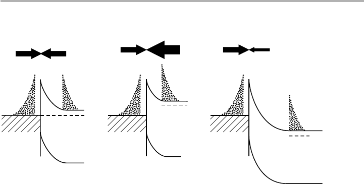
which pins the Fermi level and induces band bending. As indicated in figure 8.1 for an
n-type semiconductor, the bands bend upwards towards the interface. This bending is
associated with a dipole layer beneath the surface corresponding to the depletion
260

region, where the n-type impurities are ionized, and the surface states are negatively
charged. For a p-type semiconductor, band bending is reversed and surface states are
charged positively, as indicated earlier in figure 1.23(a). If the semiconductor is in
contact with a metal, the Fermi level is fixed by the metal, so that band bending or band
flattening can be induced depending on changes from the previous surface state distri-
bution.
The main electrical effects of this band bending arise from the asymmetry in the
current flow under bias, as shown in figure 8.1. In the conduction band, the electron
energy distribution corresponds to the tail of the Fermi function, so that at the
Schottky barrier height
f
B
, the number of electrons above the barrier scales as
exp[2(q
f
B
/kT)], where q is the (effective, positive) electron charge. In the equilibrium
case, when the Fermi levels are equal on both sides of the junction, the energy distri-
butions above the barrier must be the same, and the current flow has to be zero, as indi-
cated in figure 8.1(a). However, under bias voltage V, there is current flow. Using the
formulae for thermionic emission over the barrier (see section 6.2), we have a current
density J, given by
J5J
sm
2J
ms
5A*T
2
exp[2(q
f
B
/kT)]{exp(qV/kT)21}, (8.1)
where the ‘Richardson constant’, A* for the barrier, depends on the details of band
structures and interface chemistry. The rectifying character of the contact is deter-
mined by the asymmetry with respect to 6V, shown schematically in figures 8.1(b) and
(c). For forward bias (positive V) the current J
sm
can increase without limit, but under
reverse bias, the current is limited to a low constant value J
ms
by the Schottky barrier
height
f
B
. For higher reverse bias, catastrophic breakdown can occur.
This topic has a very long history, starting with the discovery of rectifying proper-
ties by Braun in 1874, and the use of ‘cats’ whiskers’ as detectors in the early days of
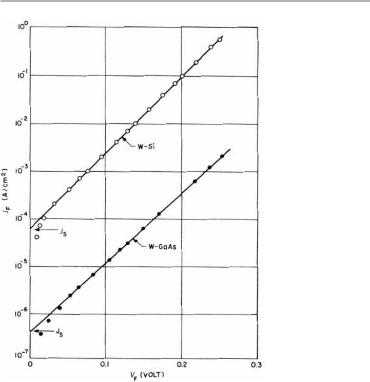
radio (Mönch 1990, 1994). The two classical means of checking (8.1) are given by Sze
(1981). Figure 8.2 is a log–log plot of the forward bias current density J
F
as a function
8.1 Metals and oxides in contact with semiconductors 261
Figure 8.1. Band bending at the surface of an n-type semiconductor under different biassing
conditions: (a) thermal equilibrium; (b) forward bias; (c) reverse bias.
(a)
(b) (c)
E
F
E
F
E
C
E
V
E
J
ms
J
sm
J
sm
J
sm
J
ms
J
ms
F

of V
F
, which gives a straight line whose slope is q/kT (Crowell et al. 1965). If q turns
out not to be equal to e, the charge on the electron, then so be it. Device engineers
replace q by q/n, where n is referred to as an ‘ideality factor’, with typical values of n5
1.02 to 1.04; i.e. the approximation that q5e is pretty good, but ‘non-ideality’ can be
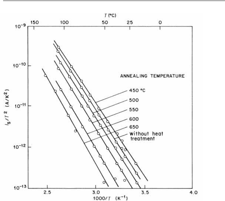
used to cover several types of disagreement with this simple model. An Arrhenius plot
of the reverse barrier current I
S
, as (log I
S
/T
2
) versus T
2
1
shown in figure 8.3, shows
that both A* and
f
B
for the important Al–Si diodes depend on processing conditions
(Chino 1973). This sensitivity to cookery has plagued the field for a long time; both
recipes and theories have on occasion become so complex as to be completely unbe-
lievable. But, before discussing these points, the next topic is the width of the depletion
region.
262 8 Surface processes in thin film devices
Figure 8.2. Logarithmic plot of forward current density J
F
versus forward voltage V
F
of
W–Si and W–GaAs diodes (from Crowell et al. 1965, after Sze 1981, reproduced with
permission).

8.1.2 Simple models of the depletion region
Models of the depletion region are well developed in the literature, and to dwell on
these here would take us too far from the topic of ‘surface processes’. The important
point to determine is the length scale over which (electron or hole) depletion is
observed, and to establish the connection with electrical and optical properties. The
key concept is screening, which was introduced briefly in section 1.5, and the closely
related values of the (relative) dielectric constant
«
. Screening is very effective in metals,
with screening lengths ⬃ (2k
F
)
21
, and moderately strong, but dependent on the doping
level, in semiconductors. It is weak in insulators, where for example it depends on ionic
defects in crystals such as NaCl, and photographic materials including AgBr. In
metals, Lindhard screening is required to describe the resulting Friedel oscillations (see
section 6.1), but in semiconductors and insulators, classical Thomas–Fermi screening
provides a sufficient description.
Consider a potential V(z) away from the surface, where the zero of V is in the bulk
8.1 Metals and oxides in contact with semiconductors 263
Figure 8.3. Arrhenius plot of the barrier current (I
S
/T
2
) of Al–Si Schottky barrier diodes
under reverse bias for different processing conditions (from Chino 1973, after Sze 1981,
reproduced with permission).

of the crystal, and an associated charge density
r
(z). This charge density may consist
of both ionized donors and acceptors, whose values are N
D
1
and N
A
2
respectively, and
the electron and hole density, n(z) and p(z), whose values are n
b
and p
b
in the bulk. In
the bulk, the charges have to be compensated, so that N
D
1
– N
A
2
5n
b
2 p
b
. The elec-
tron and hole charge distribution is biased in the presence of V(z), which is different
from zero near the surface, and gives
r
(z)51q[n
b
(exp(2qV(z)/kT)21) 2p
b
(exp(1qV(z)/kT) 21)]. (8.2)
Note that the positive sign arises because the donor and acceptor distributions stay the
same, while the electron and/or hole distribution responds to V(z); care is needed with
signs throughout this argument, which takes the electron to have q52e.
Equation (8.2) needs to be solved self-consistently, which is done within classical
electrostatics using the Poisson equation
d
2
V(z)/dz
2
52
r
(z)/
««
0
. (8.3)
This can be solved numerically, but is typically expressed within one of two limiting
approximations, for either n- or p-type semiconductors, i.e. when N
D
..N
A
or vice
versa. In the weak space charge approximation, we make a linear approximation to the
exponentials in (8.2) which gives
r
(z)5(n
b
or p
b
)q
2
V/(
««
0
kT), (8.4)
where we use n
b
or p
b
for n- or p-type doping. This results in V(z)5V
s
exp (2z/L), where
V
s
is the potential at the surface; the screening length L is given by
(Lq)
2
5(
««
0
kT)/(n
b
or p
b
). (8.5)
In the other limit we acknowledge that if V
s
is large compared to kT, then
r
(z) will
approximate to a step function, such that all the charges are ionized up to a depth d
below the surface, i.e.
r
(z)5q(N
D
or N
A
) for 0,z,d. Integrating (8.3) twice then gives
a quadratic dependence:
V(z)52q(N
D
or N
A
)(d2z)
2
/(2««
0
), (8.6)
for 0,z,d, with V(z)50 for z$d, which is known as the Schottky approximation, see
figures 8.4(b) and (c). A detailed discussion with examples is given by Lüth (1993/5,
chapter 7).
The key point is to realize how the screening length L and depletion length d depend
on the doping level in typical semiconductors. Inserting a set of values into (8.5), for
Si with
«
511.7 or Ge with
«
516, a low doping level n
b
510
20
m
23
(or equivalently 10
14
cm
23
) gives L5410 nm for Si and 480 nm for Ge. However, for a typical surface poten-
tial V
s
50.8 V, the depletion length d is greater than 3 mm; since d.L the Schottky
model is most appropriate. These lengths are very long relative to atomic dimensions;
although they will decrease as (n
b
or p
b
) increase, they are much greater than 10 nm, at
least until samples are heavily doped, and have properties approaching those of metals.
Thus it is not surprising that models of the electrical behaviour of semiconductors are
typically not unduly concerned with atomic scale or surface properties. On the other
264 8 Surface processes in thin film devices

hand, as devices get smaller, such effects can be pervasive throughout the whole device,
and the unwanted statistical distribution of impurities may well pose a limit to device
dimensions in future.
8.1.3 Techniques for analyzing semiconductor interfaces
Classical experiments to determine the depth of the depletion layer and the barrier
heights include C–V profiling, where the same types of arguments as used above show
that C
2
2
is linearly proportional to the bias voltage V, with an intercept which gives
f
B
,
and the photo-electron yield or photocurrent, where the square root of the yield versus
photon energy gives a straight line with intercept
f
B
(Sze 1981, Schroder 1998). By
biasing the sample with a d.c. offset, and using a.c. techniques for probing and detect-
ing, more subtle techniques including deep level transient spectroscopy (DLTS) have
been developed, and used to study the distribution of electrically active defects with
depth. An example related to point defects produced during InGaAs thin film growth
is given by Irving & Palmer (1992); but it is noticeable that deductions about the nature
of the defects responsible are at best rather indirect.
Semiconductor devices are very demanding in terms of analytical techniques, since
one would like to know the density and depth distribution of the dopants, and of other
impurities (Schroder 1998). Of the wide range of surface analytical techniques avail-
able, so far only secondary ion mass spectrometry (SIMS) has been widely applied;
although it is destructive, it does have the necessary sensitivity, and it specifically iden-
tifies the elements in question. The calculation in section 8.1.2 above can be used to
estimate the sensitivity needed: to detect 10
14
cm
23
dopants in a depletion layer of
thickness 400 nm, over 1 mm
2
sample area means detecting and quantifying 4310
7
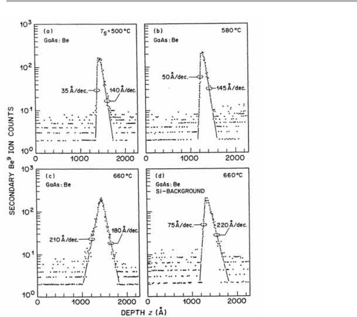
atoms. A determination of the depth distribution of (delta-doped) Be dopants in GaAs
by SIMS is shown in figure 8.5. Note that deductions about the effects of annealing
temperature and ‘knock-on’ effects during implantation have been made (reliably) from
profiles containing a maximum of only 200 counts/channel (Schubert 1994).
Although STM and related spectroscopies (STS) have revolutionized surface
imaging since the early 1980s, it is perhaps less clear whether similar advances in
8.1 Metals and oxides in contact with semiconductors 265
Figure 8.4. Depletion layer below an n-type semiconductor surface: (a) band bending showing
ionized donors above the Fermi level E
F
; (b) charge density
r
(z); and (c) potential variation
V(z) in the Schottky approximation.
(a)
(b)
(c)
E
F
+
+
+
+
o
o
oo
z
d
eN
D
Vz()
ρ()z
d
V
s
dLor
z

imaging buried interfaces, such as delta-doped layers, can be made. However, ex situ
TEM/HREM and diffraction are very powerful, and have been widely applied to semi-
conductor interfaces. There are several related techniques including Fresnel (out of
focus) imaging, which can image layers in profile with ML precision (Shih & Stobbs
1991). Convergent beam electron diffraction (CBED, see figure 3.1(d)) and convergent
beam imaging (CBIM) are powerful means of measuring small strains and distortions
in multilayers (Humphreys et al. 1988). In situ studies of reactions in UHV are very
demanding research projects, which have been pursued by relatively few groups; but
semiconductor interfaces have been prime targets for the application of these tech-
niques (Yagi 1993, Ross et al. 1994, Gibson et al. 1997, Collazo-Davila et al. 1998,
Marks et al. 1998).
One new STM-based technique has enabled some relevant device oriented studies to
be performed on a microscopic scale, as described below. This variant, known as bal-
listic energy emission microscopy (BEEM) was invented in the late 1980s (Kaiser & Bell
1988, Bell & Kaiser 1988). Reviews of this rapidly developing area have been given by
Prietsch (1995), by Bell & Kaiser (1996) and von Känel et al. (1997). The schematic
266 8 Surface processes in thin film devices
Figure 8.5. SIMS profile of Be delta-doped GaAs grown by MBE at: (a) 500, (b) 580 and
(c) 660°C; (d) inclusion of Si background doping reduces the segregation of Be to the surface
(after Schubert 1994, reproduced with permission).
