Shani G. Radiation Dosimetry: Instrumentation and Methods
Подождите немного. Документ загружается.

380 Radiation Dosimetry: Instrumentation and Methods
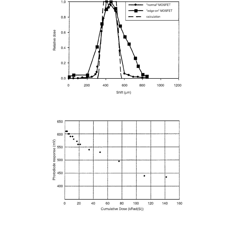
the photodiode response in terms of cumulative dose (Si)
to the 20-MeV electron field is shown in Figure 8.32. It
can be seen that after a dose of 50 krad, which is the
ionization dose expected within the BELLE SVD per
year in a worst-case scenario, the response is degraded
by ~15%.
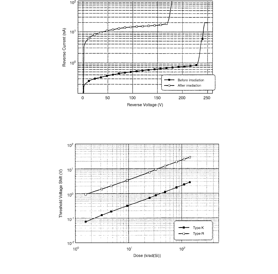
In Figure 8.33, the reverse current measured under full
depletion conditions before and after electron irradiation,
with
e
~ 10
12
e/cm
2
, is plotted as a function of reverse
voltage. Following irradiation, the reverse current
increased by a factor of ~13. The reverse current was
monitored as a function of time to determine the effects
of room temperature annealing. Over a period of two
months, the reverse current was seen to decrease by 35%
from the value measured 5 hrs after electron irradiation.
All measurements were made at a constant temperature
of 20°C.
The radiation damage of the detector is measured by
an increase in the reverse bias current per unit volume of
fully depleted detector, according to Equation 8.9:
(8.9)
where
is a current damage parameter which is depen-
dent on the type and energy of radiation
I
0
reverse current before irradiation
I reverse current after irradiation
Vol full depletion volume of the detector.
FIGURE 8.31 Comparison of transverse radiation dose profile across the 200-
m-wide microbeam measured by the MOSFET
detector in both ‘‘normal’’ and ‘‘edge-on’’ orientations. (From Reference [18]. With permission.)
FIGURE 8.32 Hamamatsu photodiode response to a 20-MeV electron field as a function of absorbed dose. (From Reference
[19]. With permission.)
II
0
Vol
--------------
p
p
Ch-08.fm Page 380 Friday, November 10, 2000 12:03 PM
Solid-State Dosimeters 381
To obtain calibration curves for the RADFET system
under high-energy electrons in terms of dose in Si, four
such devices were exposed to the 20-MeV electron field,
together with the Si photodiode and PIN dosimeter diodes.
The shift of the threshold voltage under a constant current
corresponding to the thermal stable point was measured.
All measurements were done during the 3-hour irradia-
tion. The spread in the change in threshold voltage (V
TH
)
as a function of the dose in silicon (D(Si)) was found to
be less than 3% for different RADFETs from the same
batch. Figure 8.34 shows the calibration curves for both
‘‘R’’ and ‘‘K’’ type RADFETS in the 20-MeV electron
field in terms of dose in Si. The analytical expression
derived from the calibration curves for the ‘‘K’’ type
RAFET is D 40.23 (V
TH
), where D is the dose
measured in krad(Si) and V
TH
is the voltage shift in volts.
For the ‘‘R’’-type RADFETs, D 1.81 (V
TH
).
III. P-TYPE SEMICONDUCTOR DOSIMETER
MOSFETs have a disadvantage of a response which is
dependent upon the incident photon energy, particularly
at low energies. In recent years,
p-FET dosimeters have
been developed with specially-grown thick-gate oxides
which have a large number of oxide traps. Sensitivities of
10 mV/rad(Si) have been achieved. The sensitivity to
radiation can be enhanced by applying a large positive
bias during radiation, which forces more of the positive
FIGURE 8.33 Detector reverse current measured before and after 20-MeV electron irradiation at a fluence.
e
9.2 10
11
cm
2
.
(From Reference [19]. With permission.)
FIGURE 8.34 Calibration curves for the RADFETs in terms of dose in Si. (From Reference [19]. With permission.)
Ch-08.fm Page 381 Friday, November 10, 2000 12:03 PM
382 Radiation Dosimetry: Instrumentation and Methods
oxide charge to the interface. The sensitivity to tempera-
ture can be minimized by operating the p-FET with a
current at the temperature-independent point. The main
limitation in using silicon semiconductor detectors is
effects caused by radiation damage. A nonlinear response
with dose rate has proved to be serious for n-type detectors
when pre-irradiated to 10 kGy or more in 20-MeV elec-
trons. A sensitivity drop after pre-irradiation is another
effect which is more pronounced for n-type detectors com-
pared to p-type detectors of the same resistivity. A third
effect of radiation damage is the sensitivity increase with
increasing temperature. [20]
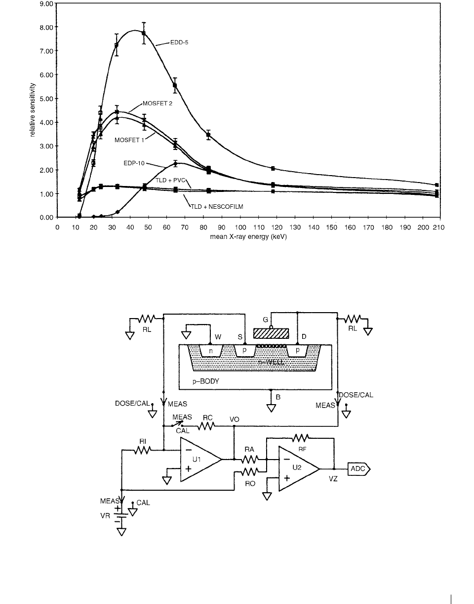
A Pantak HP-320 quasi-monoenergetic x-ray unit was
used by Edwards et al. [21] to determine the response
of two Thomson and Nielson TN-502RD MOSFETs, a
Scanditronix EDP-10 semiconductor (build-up cap 10 mm:
tissue equivalence), a BDD-5 semiconductor (build-up
cap 4.5 mm: tissue equivalence), and a LiF:Mg:Ti TLD
over the energy range 12–208 keV. The sensitivity of
each detector was normalized to the value produced by
exposure to 6-MV x-rays. The maximum relative sensi-
tivities of the two MOSFET detectors were 4.19
0.25
and 4.44 0.26, respectively, occurring at an incident
x-ray energy of 33 keV. The maximum relative sensitiv-
ity of the Scanditronix EDP-IO of 2.24 0.13 occurred
at 65 keV, and for the EDD-5, it was 7.72 0.45 at 48 keV.
The TLD produced a maximum relative sensitivity of 1.31
0.09 at 33 keV. Compared with available data based on
heteroenergetic x-ray sources, these measurements have
identified a more representative response for each detector
to low-energy x-rays.
Scanditronix
p-type semiconductor detectors were
investigated (Scanditronix, Uppsala, Sweden). These
included the EDD-5 and the EDP-IO, both connected to
a DPD-510 direct patient dosimeter. The 0.9-mm sensitive
volume of the EDD-5 detector is encapsulated by Perspex,
which provides an effective tissue-equivalent depth of
4.5 mm. This detector is designed primarily for critical
organ measurements outside the main beam. The 0.9-mm
3
sensitive volume of the EDP-IO detector is surrounded by
a 0.75-mm-thick stainless steel cap (providing a tissue-
equivalent depth of 10 mm) and is adhered to a Perspex
plate (1-mm thickness). This detector is designed for mea-
surements inside the main beam generated by 4–8 MV
linear accelerators.
A correction factor U
d
for each detector d was calcu-
lated to allow for the small difference between the SSD
to the center of its sensitive volume (J
d
) and the SSD to
a rigid surface:
(8.10)
The sensitivity
S
X,d
of a detector at each x-ray energy
relative to that produced by 6-MV x-rays was calculated
from:
(8.11)
where
R
x,d
is the detector response, b
d
is the response to
background radiation, k
x
is the kerma rate recorded by the
NE2550 Protection Level Secondary Standard with a beam
current of 1 mA and SSD of 1 m, and t
x
is the exposure time.
The corrected response per unit air-kerma rate was normal-
ized to the detector’s response per unit air kerma rate from a
6-MV linear accelerator by multiplying by two previously
determined calibration factors. The first factor L
d
converted
each detector’s response to the absolute dose rate, measured
at the maximum depth dose in a water phantom irradiated at
an SSD of 1 m with a 10-cm 10-cm field from a 6-MV
linear accelerator. The second factor
M
d
converted this to the
corresponding air-kerma rate and included any effects due to
attenuation within the detector and from backscatter.
The variation in relative sensitivity of each detector with
x-ray energy is illustrated in Figure 8.35. Relative to its
response to a 6-MV linear accelerator beam, the sensitivity
of each detector increased as the x-ray energy decreased
until it reached a maximum value, and then it decreased
with further decrease in x-ray energy.
On-chip p-FETs were developed by Buehler et al. [22]
to monitor the radiation dose of n-well CMOS ICs by
monitoring threshold voltage shifts due to radiation-
induced oxide and interface charge. The design employs
closed-geometry FETs and a zero-biased n-well to elimi-
nate leakage currents. The FETs are operated using a
constant current chosen to greatly reduce the FETs’ tem-
perature sensitivity. The dose sensitivity of these p-FETs
is about 2.6 mV/krad(Si) and the off-chip instrumenta-
tion resolves about 400 rad(Si)/bit. When operated with a
current at the temperature-independent point, it was found
that the pre-irradiation output voltage is about 1.5 V,
which depends only on design-independent silicon mate-
rial parameters. The temperature sensitivity is less than
63
V/°C over a 70°C temperature range centered about
the temperature insensitive point.
The schematic cross section of the device shown in
Figure 8.36 indicates that the n-well and source are sep-
arated so that they can operate at slightly different biases
required by the operational amplifier, U
l
. This allows all
the forced current to flow through the p-FET channel.
Drain-to-well leakage is shunted to ground. Grounding
the n-well is a departure from normal CMOS circuit oper-
ation, where the n-well is normally connected to VDD.
In operation, all terminals of the p-FET are operated
near ground except the drain, which operates near V0
1.5 V. During irradiation, the device is biased in the off state.
The two RL resistors are used to bleed off any charge
U
d
0.4
J
d
-------
2
S
x,d
L
d
M
d
R
x,d
b
d
()
k
x
t
x
A
x
F
x
U
x
-----------------------------------------
Ch-08.fm Page 382 Friday, November 10, 2000 12:03 PM
Solid-State Dosimeters 383
remaining on the p-FET. The instrumentation is calibrated
by positioning the switch to CAL, shown in Figure 8.36.
This replaces the p-FET with calibration resistor RC.
The threshold voltage is described by:
(8.12)
where D is the dose, VT
0
is the threshold voltage at T
0
and
D 0, VT
T
VT T | and .
The temperature and dose dependence of
(transconduc-
tance) is given by:
(8.13)
FIGURE 8.35 The relative sensitivity S
x
,
d
(response per unit air-kerma rate) normalized to that produced by 6-MV x-rays of two
MOSFET
p-type semiconductor diodes (EDP-10 and EDD-5) and two LiF:Mg:Ti TLD (one in PVC, one in Nescofilm™) to low-
energy quasi-monoenergetic x-rays (error bars are
1 SD). (From Reference [21]. With permission.)
FIGURE 8.36 p-FET total dose circuitry. (From Reference [22]. With permission.)
VT VT
0
VT
T
TT
0
()VT
D
D
TT
0
→
VT
D
VT
D
D 0→
0
T T
0
()
n
D
D
Ch-08.fm Page 383 Friday, November 10, 2000 12:03 PM
384 Radiation Dosimetry: Instrumentation and Methods
where
0
is
evaluated at T
0
and D 0,
D
,
n characterizes the mobility temperature dependence, and
T is the absolute temperature. , KP
C
0
. W
e
W DW and L
e
L DL are the effective
channel width and length, respectively,
is the zero field
channel mobility, C
0
is the gate oxide capacitance per unit
area.
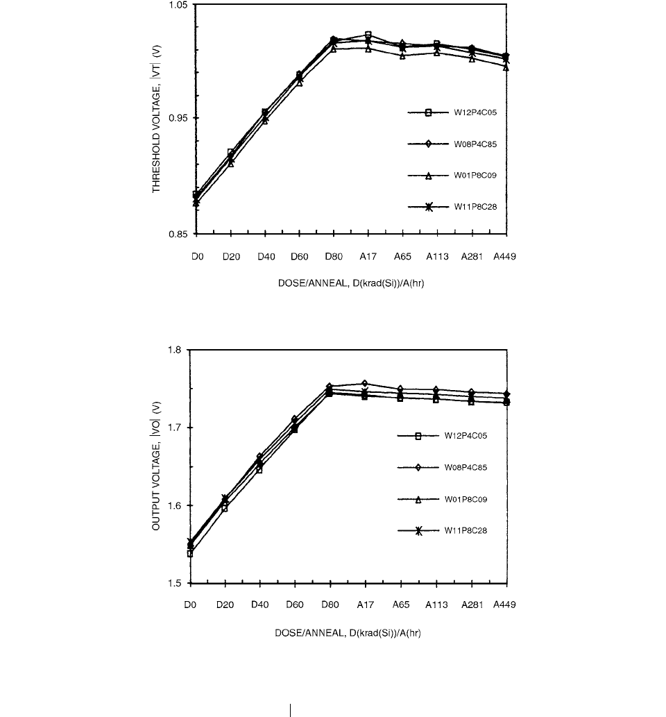
The VT values, plotted in Figure 8.37, show a high degree
of linearity during irradiation and a slight recovery with anneal.
The group average slope of the VT vs. dose curve during
irradiation is VT
D
1.698 0.038 mV/krad(Si). The shift
in VT with radiation is consistent with the build-up of positive
oxide charge and interface states. The slight recovery of VT
during room-temperature anneal is consistent with the slight
loss of oxide charge. The interface state density is stable, as
seen by the flat response of the mobility during anneal.
The output voltage for the four p-FET samples is
shown in Figure 8.38. This plot was obtained from data
sets. The data shows a nearly linear rise in V
0
with dose
and a slight annealing effect.
Brucker et al. [23] present the results of studies of
dose enhancement in dual and single dielectric pMOSFET
dosimeters for various package and die designs. Eight
different MOSFET designs and package types were inves-
tigated over a photon energy range from 14 to 1250 keV.
Packages filled with silicon grease, aluminum oxide, or
FIGURE 8.37 Four 1.2-
m CMOS p-FET threshold voltage dose/anneal responses. (From Reference [22]. With permission.)
FIGURE 8.38 Four 1.2-
m CMOS p-FET output voltage dose/anneal responses determined at the current, ID
m
. (From Reference
[22]. With permission.)
D
D 0→
KP W
e
L
e
Ch-08.fm Page 384 Friday, November 10, 2000 12:03 PM
Solid-State Dosimeters 385
paraffin eliminated the contribution of back scatter to the
enhanced dose. These modifications allowed measure-
ments of the usual dose enhancement at the aluminum or
polysilicon gate-silicon nitride (dual dielectric devices) or
silicon dioxide interfaces (single dielectric parts) and at the
silicon nitride–silicon dioxide interface. In addition to the
primary peak in the DEF (dose enhancement factor) curve
vs. energy at 45.7 keV, there is a second peak at about 215
keV. This peak might be due to enhancements at the inter-
faces of a MOSFET. These interface effects were small in
the single-insulator parts in standard ceramic packages and
significantly larger in the dual-insulator devices. The
effects were reduced by filling the packages with the mate-
rials as previously described. The geometry of the package,
the size of the air gap between the die’s surfaces, and the
lid of the package impacts the value of the DEF.
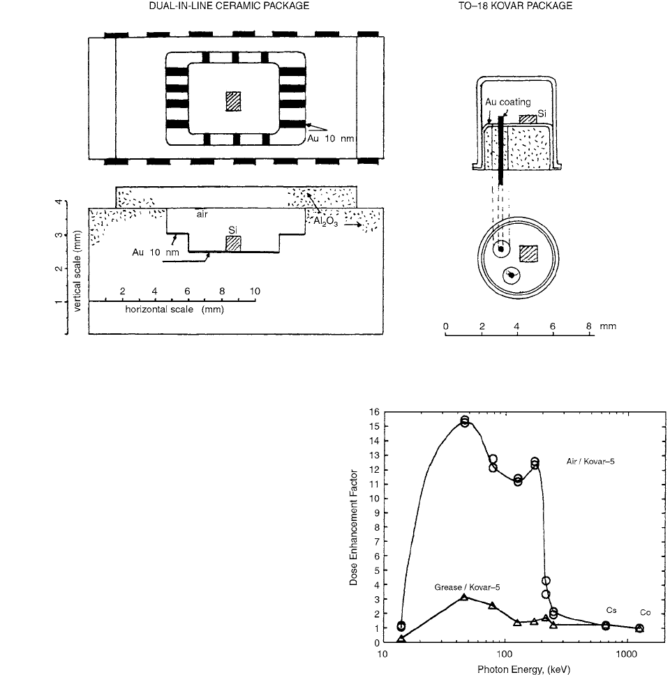
The three-dimensional models used by the code were
those in Figure 8.39. The figure shows a cross-sectional and
top view of the dual-in-line ceramic and TO-18L kovar can
packages. The gold coatings on the bonding pads and in
the well or cavity of the ceramic package are indicated. This
diagram actually represents the REM 501A part type. The
other REM devices did not have the coating in the cavity.
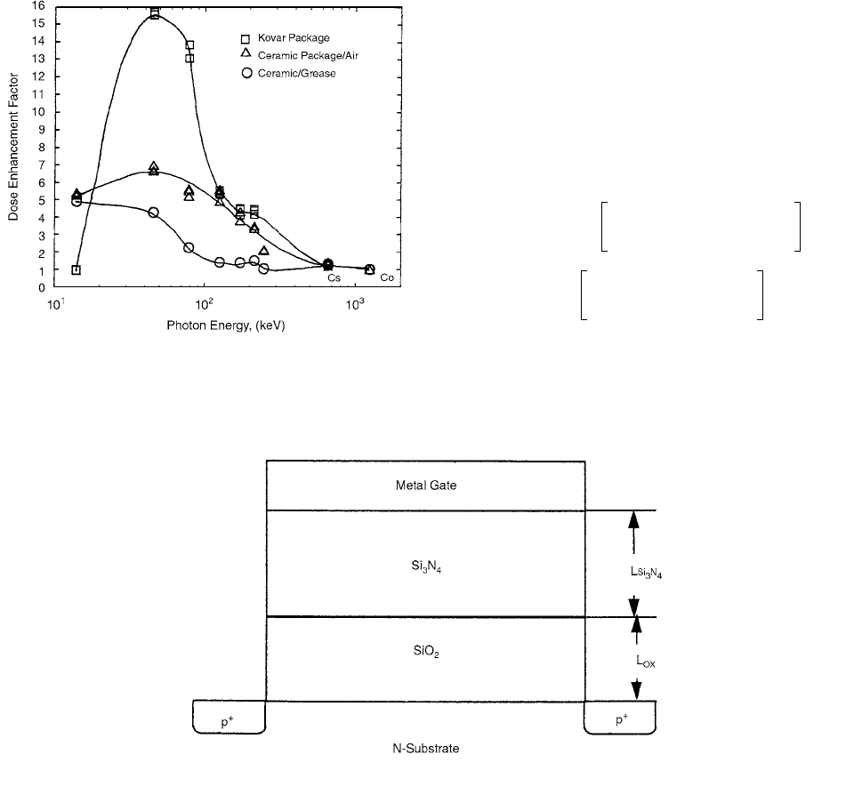
Figure 8.40 shows a comparison of results obtained with
air- and grease-filled TO-5 kovar cans containing #3 transis-
tors. Figure 8.41 contains plots that compare the DBF values
for Sandia #l parts in ceramic and kovar packages. Results
for air- and grease-filled ceramic packages are also shown.
A dose-rate-independent p-MOS dosimeter for space
applications was discussed by Schwank, et al. [24] A dual
dielectric p-MOS dosimeter (RADFET) has been designed
at Sandia. The RADFET consists of a thermally grown
oxide and a CVD deposited nitride. With a negatively
applied bias, holes generated in the SiO
2
transport to and
are trapped at the SiO
2
/Si
3
N
4
interface, producing a mea-
surable threshold-voltage shift. Because holes are trapped
away from the Si/SiO
2
interface, hole neutralization by
tunneling and interface-trap build-up are minimized, result-
ing in little fade or annealing of the RADFET output
response. RADFETs were irradiated at dose rates from
0.002 to 50 rad(Si)/s, with biases from 5 to 20 V.
FIGURE 8.39 Cross-sectional and top views of dual-in-line ceramic and TO-18L kovar can packages. (From Reference [23]. With
permission.)
FIGURE 8.40 Dose enhancement vs. energy for Sandia #3 in
TO-5 kovar cans with and without grease in package. (From
Reference [23]. With permission.)
Ch-08.fm Page 385 Friday, November 10, 2000 12:03 PM
386 Radiation Dosimetry: Instrumentation and Methods
RADFETs were also annealed for times up to 10
7
s at
temperatures up to 100°C. Within experimental uncertainty,
no difference in RADFET output response at a given bias
was observed over the dose rate range examined and for
25°C anneals. At an anneal temperature of 100°C, only a
20% decrease in RADFET output response was observed.
To monitor total dose, RADFETs were characterized
for the threshold-voltage shift, V
TH
, and the change in
source-to-drain voltage, V
DS
, necessary to maintain a
constant source-to-drain current, I
DS
.
The RADFETs were designed at Sandia and fabricated
at Micrel Semiconductor Corporation. The structure of the
RADFET is shown in Figure 8.42. The RADFETs used by
Schwank et al. consisted of a 60-nm thermal oxide grown
on a (100) n on n
expitaxial substrate, and a low-pressure
CVD 100-nm silicon nitride layer deposited on top of the
oxide. All RADFETs were p-channel transistors with
metal gates and were taken from the same wafer. The
wafer-to-wafer and lot-to-lot variation in RADFET
response is not known, so other wafers would have to be
calibrated independently. Transistors were packaged in
24-pin DIP packages.
p-MOS dosimeters with a single dielectric have been
fabricated using a variety of techniques. Most of these
measure the threshold-voltage shift induced by positive
charge trapping in the oxide. For thermal oxides, most of
the trapped charge occurs in the oxide near either the top
gate-Si/SiO
2
(negative gate bias during irradiation) or
bottom Si/SiO
2
(positive gate bias during irradiation)
interface. If holes are trapped near the top interface,
the measured threshold-voltage shift is very small, due
to a small charge moment arm. For this reason, standard
p-MOS dosimeters are normally operated with a positive
applied bias. Unfortunately, for positive applied biases,
interface traps will be generated at the Si/SiO
2
interface
and trapped holes can be neutralized by thermal emission
and tunneling processes. The time dependence of interface-
trap build-up and the neutralization of holes will result in
fade of the dosimeter’s output characteristics. [24]
The radiation-induced threshold voltage shift, V
TH
,
of Sandia’s dual dielectric RADFET is given by:
(8.14)
where
oX
and are the dielectric constants for SiO
2
(
3.9) and Si
3
N
4
(
7.5), respectively,
0
is the
permittivity of free space, L
oX
is the thickness of the oxide
layer, L
T
is the total dielectric thickness (SiO
2
Si
3
N
4
),
FIGURE 8.41 Illustrates effect of package and filling in reduc-
ing DBF for Sandia #l in TO-18L and ceramic FLTPAC. (From
Reference [23]. With permission.)
V
TH
L
ox
ox
0
------------
q
L
ox
-------
L
ox
x()n
h
x() xd
0
L
ox
L
T
L
ox
Si
3
N
4
0
---------------------
qn
h
x() xd
0
L
ox
Si
3
N
4
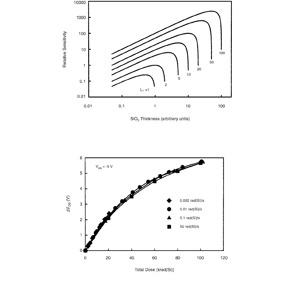
FIGURE 8.42 RADFET transistor structure. (From Reference [24]. With permission.)
Ch-08.fm Page 386 Friday, November 10, 2000 12:03 PM
Solid-State Dosimeters 387
and n
h
(X) is the distribution of trapped holes in the SiO
2
layer (or net positive charge if both electrons and holes
are trapped). x is measured relative to the metal gate/Si
3
N
4
interface.
Figure 8.43 is a plot of calculated relative radiation
sensitivity vs. SiO
2
thickness for several values of insula-
tor thickness (SiO
2
Si
3
N
4
).
At very low temperatures (~100°K), holes generated
in the SiO
2
will be immobile and the distribution of holes
throughout the SiO
2
is uniform. Under these conditions,
the radiation sensitivity is proportional to
(8.15)
The radiation response of the RADFETs for dose rates
from 0.002 to 50 rad(Si)/s is shown in Figure 8.44. This
figure is a plot of V
DS
for a constant source-to-drain
current (~4 mA) for RADFETs irradiated at room tem-
perature to 100 krad(Si) with a constant gate-to-source
bias, V
GS
, of 5 V.
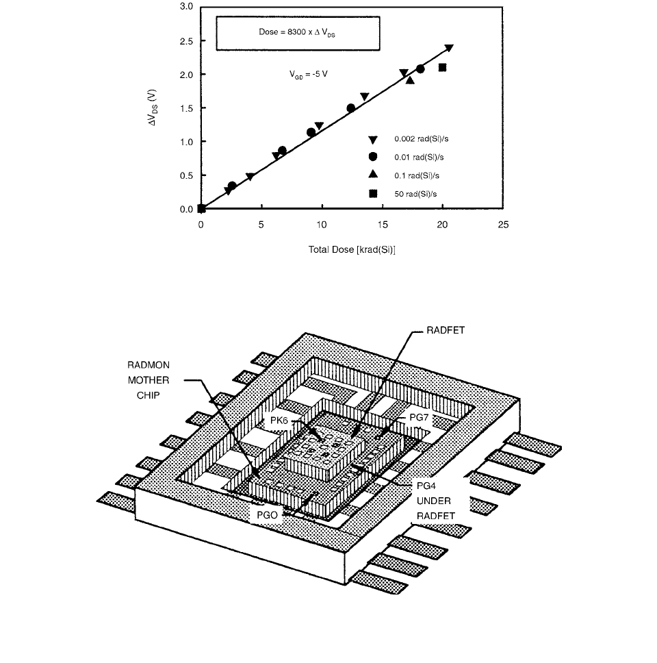
For low total dose levels, the output response of the
RADFETs is linear with total dose. Figure 8.45 is a plot
of V
DS
for RADFETs irradiated to 20 krad(Si) at dose
rates from 0.002 to 50 rad(Si)/s with V
GS
5 V. Over
this dose range, for all dose rates, the dose is given by
(8.16)
FIGURE 8.43 Relative RADFET sensitivity for the case where holes are trapped near the SiO
2
/Si
3
N
4
interface for oxide thicknesses
from 0.05 to 100 (arbitrary units) and total insulator thicknesses,
L
T
, from 1 to 100 (arbitrary units). (From Reference [24]. With
permission.)
FIGURE 8.44 V
DS
vs total dose for RADFET. (From Reference [24]. With permission.)
S
L
ox
2
2
ox
----------
L
ox
L
T
L
ox
()
Si
3
N
4
----------------------------------
Dose[rad(Si)] 8300 V
DS
Ch-08.fm Page 387 Friday, November 10, 2000 12:03 PM
388 Radiation Dosimetry: Instrumentation and Methods
where V
DS
is given in volts. At higher total doses, 20
krad(Si), the RADFET output response becomes sublinear
(see Figure 8.44) as the trapped charge in the insulator
begins to reduce the internal field in the oxide. As the oxide
electric field is lowered, the amount of electron-hole recom-
bination increases. The increase in electron-hole recombi-
nation will result in fewer trapped holes in the insulator. [24]
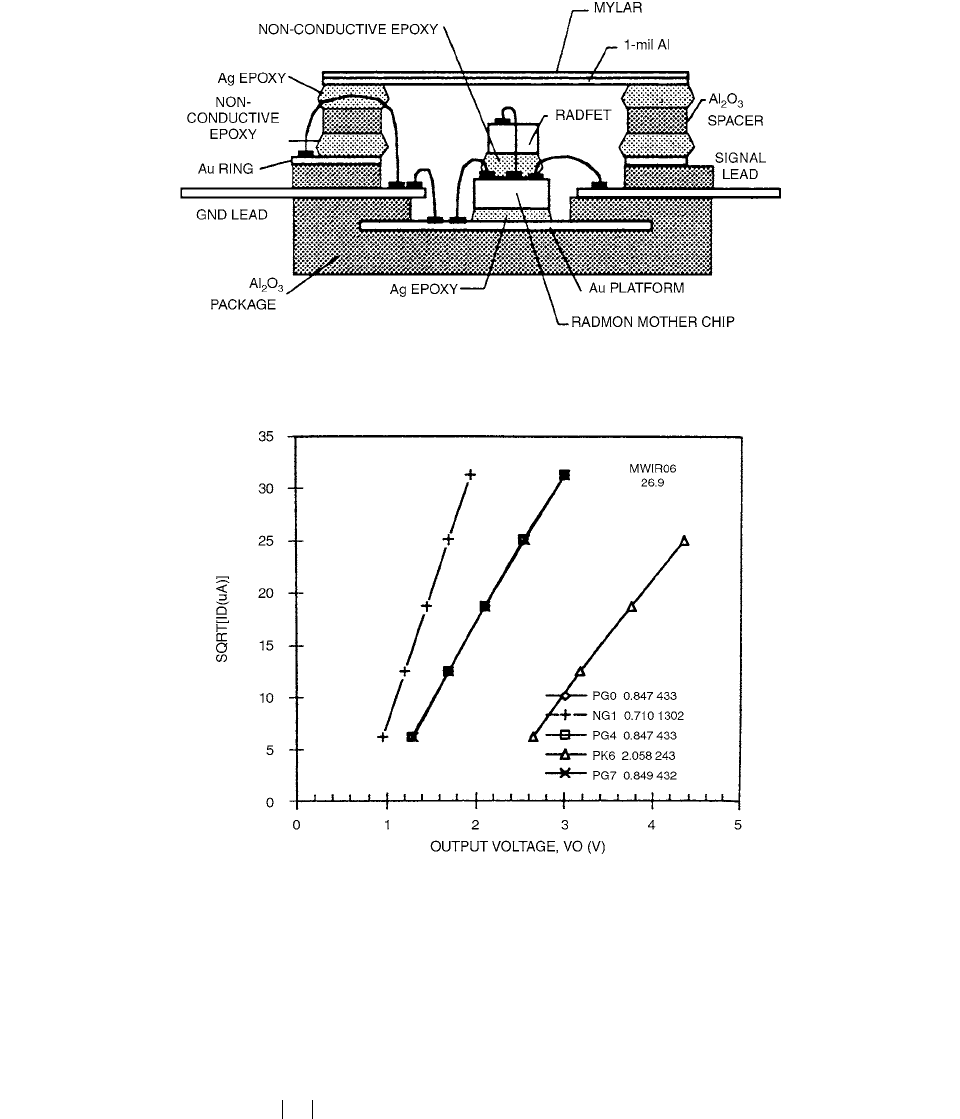
A stacked p-FET dosimeter consisting of a RADMON
mother chip with three p-FETs and multiplexer and an
attached RADFET has been developed by Buehler et al.
[25] for the STRV-2/MWIR detector. Calibration of the
dosimeter using an Am-241 source indicates that the
RADFET is about 20 times more sensitive to radiation
than the RADMON. This dosimeter is expected to mea-
sure radiation dose from rads to megarads.
The dosimeter, seen in Figure 8.46, consists of a thin-
oxide RADMON mother chip with three p-FETs, a multi-
plexer, and other devices. A thick-oxide RADFET is
attached to the mother chip. The device operates on the
principle that radiation passing through the gate oxide region
of the p-FET creates hole-electron pairs. Since the oxides
have mainly hole traps, radiation-induced positive charge is
trapped in the oxide. This build-up of positive charge
changes the threshold voltage of the device, which is inter-
preted in terms of radiation dose. A cross-section view is
shown in Figure 8.47.
FIGURE 8.45 V
DS
vs. total dose for RADFETs irradiated to 20 krad(Si) at dose rates from 0.002 to 50 rad(Si)/s with V
GS
5V.
(From Reference [24]. With permission.)
FIGURE 8.46 RADFET mounted on the RADMON mother chip in a 16-pin flat package. Three radiation sensitivities are achieved:
PK6 has highest sensitivity, PG0 and PG7 have moderate sensitivity, and PG4 has lowest sensitivity, being shielded by the RADFET.
(From Reference [25]. With permission.)
Ch-08.fm Page 388 Friday, November 10, 2000 12:03 PM
Solid-State Dosimeters 389
Room temperature current-voltage measurements are
shown in Figure 8.48 for the five FETs in this experiment.
These curves were modeled using the saturation drain
current expression:
(8.17)
where
VO is the FET output voltage,
KP W/L is
the transconductance, KP
C
0
, W is the channel width,
L is the channel length,
is the channel mobility, and C
0
is the gate oxide capacitance per unit area. The threshold
voltage, VT, is determined from the extrapolation of the
curves shown in Figure 8.48 to zero drain current using a
least-squares fitting technique. The
values were deter-
mined from the slope of the characteristics shown in
Figure 8.48.
Semiconductor detectors based on p-type silicon but
with different doping levels have been investigated by
Grusell and Rikner. [26] It was shown that a p-type detector
with a low doping level and high resistivity showed a non-
linear dose rate response if it were radiation-damaged in a
high-energy photon beam, which contains neutrons. By
increasing the doping level, it was shown that a detector
with a resistivity of 0.2 cm stayed linear after pre-irradi-
ation in radiation fields from high-energy electrons, pho-
tons, and protons. Other parameters did not show any
changes of clinical importance at the different doping levels.
FIGURE 8.47 Cross section of the MWIR dosimeter package showing the wire bonds that ground the Au ring and aluminum-coated
mylar lid
. (From Reference [25]. With permission.)
FIGURE 8.48 Typical current-voltage characteristics for the five FETs located on the MWIR. Note that the FET characteristics for
PG0, PG4, and PG7 overlap. The numbers in the key are
VT in volts and
in
A/V
2
. (From Reference [25]. With permission.)
ID
2
---
VO VT()
2
Ch-08.fm Page 389 Friday, November 10, 2000 12:03 PM