Shani G. Radiation Dosimetry: Instrumentation and Methods
Подождите немного. Документ загружается.

370 Radiation Dosimetry: Instrumentation and Methods
Using a diamond detector for the dosimetry of brachy-
therapy sources was investigated by Rustgi. [10] A high-
activity
192
Ir source was selected for this purpose. The
dosimetric characteristics measured included the photon
fluence anisotropy in air, transverse dose profiles in planes
parallel to the plane containing the HDR source, and iso-
dose distributions. The “in-air” anisotropy of the photon
fluence relative to seed orientation was measured at 5 and
10 cm from the source.
A type 60003 diamond detector manufactured by
PTW Freiburg was used by Rustgi. The radiation-sensitive
region of the diamond detector had a volume of 1.8 mm
3
.
The low-impurity diamond crystal of unknown shape had
a thickness of a 0.26 mm. The crystal was enclosed in a
plastic housing, with the surface of the crystal displaced
1 mm below the housing front surface. All measurements
were made with an external bias of 100 V, as recom-
mended by the manufacturer, to achieve near-total ion-pair
collection.
The EGS4 Monte Carlo code has been used by Mobit
and Sandison [11] to investigate the response of a PTW/
diamond detector irradiated in both clinical and monoener-
getic megavoltage electron beams ranging in energy from
5 to 20 MeV. The sensitive volume of the PTW/diamond
detector simulated has a thickness of 0.4 mm and a diam-
eter of 4.4 mm. The results show that the PTW/diamond
detector has a constant response (within 1.0%) in electron
beams if irradiated at depths closed to d
max
, and its
response is almost independent of irradiation depth or
incident electron energy (within 3%). The encapsulation
of the bare diamond detector with low-Z epoxy and poly-
styrene wall material does not affect its response in elec-
tron beams.
Figure 8.16 shows the schematic of the simulated
PTW/diamond detector (model T60003) designed to mea-
sure relative dose distributions in high-energy photon and
electron beams. The sensitive volume of the PTW/dia-
mond detector is a disk made from natural diamond (den-
sity 3.51 g/cm
3
) with a radius ranging from 1.0 to 2.2 mm
and a thickness ranging from 0.2 to 0.4 mm.
When the PTW/diamond detector is irradiated in a water
phantom at given point p, the absorbed dose to the water
phantom at this point D
w
(p), following the Spencer-Attix
cavity equation and the AAPM-TG21 protocol, is as fol-
lows:
(8.5)
where is the average absorbed dose in the sensitive
volume, of the PTW/diamond detector, is the Spencer-
Attrix mass collision stopping power ratio of water to
diamond (graphite), is the perturbation correction
factor due to the non-water equivalence of the encapsu-
lating wall material of the PTW/diamond detector, and
is the perturbation correction factor resulting from
the insertion of the diamond-sensitive volume into the water
medium, which can be considered as the perturbation due
to the departure of the wall-less (bare) detector from non-
ideal Bragg-Gray (Spencer-Attix) conditions. Here,
in the TG21 formulation is regarded as the product of two
perturbation correction factors, the electron fluence per-
turbation correction factor and the dose gradient pertur-
bation correction factor.
Since the sensitive volume of the PTW/diamond
detector is very small (6.1 mm
3
), one can assume that the
FIGURE 8.15 Response of diamond detector at photon energies of 4, 6, 15, and 25 MV ( , right axis). For comparison, the average
mass stopping power ratio of water/carbon and of water/air (left axis) is drawn in. (From Reference [9]. With permission.)
I
D
w
p() D
PTW
s
w,dia
SA
P
cav
PTW
P
wall
PTW
N
PTW
D
PTW
s
w,dia
SA
P
wall
PTW
P
cav
PTW
P
cav
PTW
Ch-08.fm Page 370 Friday, November 10, 2000 12:03 PM

Solid-State Dosimeters 371
absorbed dose in the water phantom at point p is equal to
the absorbed dose to the water phantom averaged over the
same volume as the cavity. This means D
w
(p) , and
Equation (8.5) can be written as
(8.6)
where is the average absorbed dose in water of the
same volume, as the wall-less diamond detector placed at
the same point p is the uniform water phantom.
The PTW/diamond detector response depends on
the average absorbed dose ratio of water to diamond
, and this ratio can be used to determine if the
PTW/diamond detector response depends on the depth of
irradiation or the incident electron beam energy. Table 8.2
shows the average absorbed dose ratio of water to the
sensitive volume of the PTW/diamond detector (
) for incident monoenergetic electron beams.
For wall-less detectors like TLDs, the deviation of the
absorbed dose at a point p in a uniform medium, from the
Spencer-Attix cavity equation, can be expressed as:
(8.7)
where is the perturbation correction factor,
is the average absorbed dose ratio of the
medium to cavity, and is the Spencer-Attix mass
collision stopping power ratio. However, for an encapsu-
lated diamond detector like the PTW/diamond detector,
the perturbation effects are from two different sources: (1) the
encapsulation and (2) the perturbation due to the sensitive
volume of the detector (air for ion chambers and dia-
mond for the PTW/diamond dosimeter) not acting as a
perfect Bragg-Gray cavity [Equation (8.7)]. The effect of
the encapsulation, denoted by , can be determined by
comparing the PTW/diamond response in a water phan-
tom to the response of a nonencapsulated diamond detec-
tor of identical sensitive volume (identical dimensions)
irradiated at the same depth with the same incident elec-
tron energies. [11]
TABLE 8.2
Monte Carlo–Determined Variation with Energy of the Average
Absorbed Dose Ratio of Water to the Sensitive Volume of the
PTW/Diamond Detector in Monoenergetic Electron Beams
E
O
(MeV) Depth (cm) E
d
(MeV)
5 1.2 2.2 1.145 0.002
10 2.7 4.1 1.146 0.002
15 3.6 6.7 1.149 0.002
20 5.4 7.0 1.148 0.002
The electron beam size is a square of dimension 10 cm at the phantom surface, and
the incident electron beam is assumed to be parallel and nondivergent. The mean
energy at depth (E
d
) was calculated following the IAEA method.
From Reference [11]. With permission.
FIGURE 8.16 Composition of the PTW/diamond detector (the simulated geometry).(From Reference [11]. With permission.)
D
w
/D
PTW
D
w
D
w
D
PTW
s
w,dia
SA
P
cav
PTW
P
wall
PTW
D
W
D
w
D
PTW
()
D
w
D
PTW
P
med,cav
D
med
D
cav
s
med,cav
SA
-------------------------
p
med,cav
D
med
D
cav
()
s
med,cav
SA
P
wall
PTW
Ch-08.fm Page 371 Friday, November 10, 2000 12:03 PM
372 Radiation Dosimetry: Instrumentation and Methods
II. MOSFET RADIATION DOSIMETER
MOSFET is a sandwich-type device consisting of a p-type
silicon semiconductor substrate separated from a metal
gate by an insulating oxide layer. The advantages of MOS-
FET devices include being a direct reading detector with
thin active area (25
m) and having a small size. The
signal can be permanently stored and is dose-rate inde-
pendent. Dose enhancement was observed for photon
energies below 40 keV, where the photoelectric effect is
dominant. With adequate filtration, uniform response was
reported for photon energies above 80 keV. The sensitivity
and linearity of MOSFET devices is greatly influenced by
the fabrication process and the voltage-controlled opera-
tion during and after irradiation.
When a metal-oxide-semiconductor (MOS) device is
irradiated, three mechanisms within the silicon dioxide
layer predominate: the build-up of trapped charge in the
oxide; the increase in the number of interface traps; and
the increase in the number of bulk oxide traps. Electron-
hole pairs are generated within the silicon dioxide by the
incident-ionizing radiation. Electrons, whose mobility in
SiO
2
at room temperature is about 4 orders of magnitude
greater than holes, quickly move toward the positively
biased contacts. Depending on the applied field and the
energy and kind of incident particle, some fraction of
electrons and holes will recombine. The holes that escape
initial recombination are relatively immobile and remain
behind, near their point of generation.
A negative bias applied to the FET gate causes a
positive charge to build-up in the silicon substrate. This
build-up of charge allows current to pass through the silicon
substrate from the source to the drain terminals. The gate
voltage necessary to allow conduction through the MOS-
FET is known as the threshold voltage.
When the MOSFET is exposed to ionizing, radiation,
electron hole pairs are formed in the oxide insulation layer.
The junction potential between the device layers, or an
applied positive potential to the gate, causes the electrons
to travel to the gate while the holes migrate to the oxide
silicon interface, where they are trapped. These trapped
positive charges cause a shift in the threshold voltage,
since a larger negative voltage must be applied to the gate
to overcome the electric field of the trapped charges to
achieve conduction. The threshold voltage shift is propor-
tional to the radiation dose deposited in the oxide layer,
and this relationship is the basis for using MOSFETs as
dosimeters. Irradiated MOSFETs have been stored under
zero bias condition for over ten years with approximately
1% loss of signal.
The efficiency of charge trapping or effective sensi-
tivity of the MOSFET depends on the thickness of the
oxide layer and the bias potential applied across the
layer during irradiation. For a given oxide layer thick-
ness, the sensitivity can be controlled by the bias potential
applied between the gate and substrate during irradiation,
since large electric fields applied across the oxide layer
result in more rapid separation of the electrons from the
holes.
Positive-ion diffusion toward the oxide-silicon inter-
face results in a negative shift of the threshold voltage,
while phonon-induced (thermal) release of trapped
charges, as well as charge annihilation by electrons tun-
neling from the silicon to the oxide layer (nonthermal),
results in annealing or a positive shift of threshold voltage.
These signal drifts become particularly apparent during
low dose rate, long-time irradiations. In order to obtain
meaningful dosimetric information from a MOSFET
dosimeter under low dose rate conditions, the drift effects
must be characterized and deconvoluted from the thresh-
old voltage data.
Prototype miniature dosimeter probes have been de-
signed, built, and characterized by Gladstone et al. [12],
employing a small, radiation-sensitive metal oxide semicon-
ductor field effect transistor (MOSFET) chip. It was used to
measure, in vivo, the total accumulated dose and dose rate
as a function of time after internal administration of long-
range beta particle radiolabeled antibodies and in external
high-energy photon and electron beams. The MOSFET
detector is mounted on a long narrow alumina substrate
to facilitate electrical connection. The basic MOSFET
probe design is shown in Figure. 8.17.
A plot of the sensitivity vs. bias voltage is shown in
Figure 8.18. A line is drawn through the data points, show-
ing that the sensitivity of the MOSFET detector varies
logarithmically with bias potential between 1.5 and 9 V.
The sensitivity does not change as a function of total
absorbed dose from 1 to 1000 cGy or dose rate from
0.195 cGy/h to 400 cGy/min.
Figure 8.19 is a plot of the threshold voltage vs. tem-
perature for our MOSFET probe. The threshold voltage
for this MOSFET type is linear with temperature, with a
slope of 7.4 mV/°C. This linear temperature shift is easily
characterized and corrected for by adding an offset to
account for the temperature of the MOSFET at the time the
threshold voltage is measured. If pre- and post-irradiation
measurements are made at the same temperature, no cor-
rection is needed.
The drift rate of the threshold voltage is observed
to be linear with ln (
t/t
0
) (t is time after irradiation and
t
0
is normalization time of 1 min) at times greater than
150 min, with the rate of drift increasing with increasing
temperature.
A direct-reading semiconductor dosimeter has been
investigated by Soubra et al. [13] as a radiation detector for
photon and electron therapy beams of various energies. The
operation of this device is based on the measurement of the
threshold voltage shift in a custom-built metal oxide–silicon
semiconductor field effect transistor (MOSFET). This volt-
age is a linear function of absorbed dose. The extent of the
Ch-08.fm Page 372 Friday, November 10, 2000 12:03 PM

Solid-State Dosimeters 373
linearity region is dependent on the voltage-controlled oper-
ation during irradiation. Operating two MOSFETS at two
different biases simultaneously during irradiation will result
in sensitivity (V/Gy) reproducibility better than 3% over
a range in dose of 100 Gy and at a dose per fraction greater
than 20 10
2
Gy. The modes of operation give this device
many advantages, such as continuous monitoring during
irradiation, immediate reading, and permanent storage of
total dose after irradiation.
The basic MOSFET structure is depicted in Figure 8.20.
The type shown is known as a p channel enhancement
MOSFET, which is built on a negatively doped (n-type)
silicon substrate. Two terminals of the MOSFET, called
the source (s) and the drain (d) are situated on top of a
positively doped (p-type) silicon region. The third termi-
nal shown is the gate (g). Underneath the gate is an insu-
lating silicon dioxide layer, and underneath this oxide
layer is the n silicon substrate. The region of the substrate
immediately below the oxide layer is known as the channel
region. When a sufficiently negative V
G
(gate voltage) is
applied (with reference to the substrate), a significant num-
ber of minority carriers (holes in this case) will be attracted
to the oxide-silicon surface from both the bulk of the silicon
and the source and drain regions. Once a sufficient number
of holes have accumulated there, a conduction channel is
formed, allowing an appreciable amount of current to flow
between the source and the drain (I
ds
). Figure 8.21 shows
how the magnitude of current varies with gate voltage.
FIGURE 8.17 Miniature MOSFET radiation detector probe design. The MOSFET chip is mounted on an alumina substrate. Gold
wire is used to electronically connect the MOSFET to the leads of the substrate. A cable is connected to the end of the substrate not
shown. The probe is inserted into a plastic flexineedle for protection before insertion into tissue. (From Reference [12]. With
permission.)
FIGURE 8.18 Sensitivity vs. bias voltage. The sensitivity
increases with increasing bias voltage.(From Reference [12]. With
permission.)
FIGURE 8.19 Threshold voltage vs. temperature. The magni-
tude of the threshold voltage decreases with increasing temper-
ature. (From Reference. [12] With permission.)
Ch-08.fm Page 373 Friday, November 10, 2000 12:03 PM

374 Radiation Dosimetry: Instrumentation and Methods
Threshold voltage (V
TH
) is defined as the gate voltage
needed to attain a predetermined current flow (I
ds
).
Typically commercial MOS transistors have 200- to
800-Å-thick gate oxides. To maximize the MOSFET sen-
sitivity to ionizing radiation, a relatively thick gate oxide
is preferred. However, there is a limitation to how thick a
gate oxide can be grown. Growth of extremely thick oxide
layers (l
m) requires growth times of more than 100 h
at temperatures of 1000°C. These oxidation times are not
feasible and, in addition, thick oxide will tend to be
highly stressed, leading to dislocations at the Si-SiO
2
interface, resulting in fast surface states and threshold
instability. [13]
The response of the single MOSFET detector (V
TH
) as
a function of accumulated dose will exhibit a nonlinear
region at high dose levels. The main reason for this phenom-
enon is the accumulation of the radiation-generated positive
charge (holes) in the oxide traps, which effectively reduces
the magnitude of the electric field produced by the positive
gate bias between the positive-charge region and the gate.
The MOSFET is approximately 200
m in diameter
and consists of a 0.5-
m Al electrode on top of a l-
m
SiO
2
and 300-
m Si substrate. Results for percentage
surface dose measured by Butson et al. [14] were within
2% compared to the Attix chamber and within 3% of
TLD extrapolation results for normally incident beams.
Percentage surface dose for 10 10-cm and 40 40-cm
field size for 6-MV x-ray at 100-cm SSD using the MOS-
FET was 16% and 42% of maximum, respectively. Factors
such as its small size, immediate retrieval of results, high
accuracy attainable from low applied doses, and recording
of its dose history make the MOSFET a suitable in vivo
dosimeter where surface and skin doses need to be deter-
mined.
Dose in the build-up region varies considerably with
changes in parameters such as beam energy, SSD, patient
geometry, angle of incidence, field size, and the use of
blocks, block trays, and wedges and boluses. Dose depos-
ited at the surface and in the build-up region has two main
contributors:
1. In-phantom scatter, where x-rays are incident on
the phantom and interact with electrons via
mainly the Compton effect and, to a lesser extent,
photoelectric and pair production at 6-MV x-ray
energy, which, in turn, deposit their energy along
their path; and
2. Electron contamination from electrons pro-
duced outside the phantom and incident on the
phantom to deposit their dose. These electrons
are produced by x-rays interacting with material
in and on the machine head, such as flattening
filters, ion chambers, collimators, block trays
and wedges, plus the air column between the
source and phantom. These electrons will be
referred to as electron contamination.
Skin dose measurements represent a greater technical chal-
lenge because of the small distances to superficial layers;
hence, any suitable detector should have minimal build-
up due to encapsulation.
The experimental configuration for the MOSFET con-
sisted of a scientific grade (stock item) n-type MOSFET
device from which Butson et al. have removed the nickel
casing, leaving the bare crystal intact and exposed, as
shown in Figure 8.22. This was easily achieved using
pliers to ease off the cap that was connected at three
positions around its base to the device’s main body. We
FIGURE 8.20 Schematic cross section of a p-channel MOSFET
showing the oxide (SiO
2
), the substrate (Si), the source, the gate,
and the drain. (From Reference [13]. With permission.)
FIGURE 8.21 Typical MOSFET source to drain current I
ds
vs.
gate voltage
V
gs
. The difference in the gate voltages V
gs
needed
to attain a predetermined current flow
I
ds
, before and after radi-
ation, is equal to the threshold voltage shift (
V
TH
). (From Ref-
erence [13]. With permission.)
Ch-08.fm Page 374 Friday, November 10, 2000 12:03 PM
Solid-State Dosimeters 375
refer to this state as the unencapsulated MOSFET. During
irradiation, the MOSFET was connected to a 6-V bias
voltage supplied by a DC battery with a circuit, as shown
in Figure 8.23.
The unencapsulated MOSFET has a few advantages over
the TLD:
1. Immediate retrieval. Dose can be ascertained
accurately within minutes after irradiation with
as low as 10 cGy of applied dose.
2. MOSFETs can be used again immediately.
They do not require an anneal process after
irradiation; TLDs do require such a process.
3. Inexpensive support equipment. MOSFETs
require only a small power source and voltmeter
for data retrieval.
4. MOSFETs retain their dose history. Informa-
tion is not lost during the retrieval process.
All of the above properties and their accuracy make the
unencapsulated MOSFET an ideal in vivo dosimeter for
surface and skin dose measurements.
Rosenfeld et al. [15] was concerned with the role of the
package of MOSFETs used in measurements of gamma
dose in mixed gamma-neutron fields, in high energy
bremsstrahlung, and in soft x-ray fields. It is shown that
a kovar cap should be avoided for dosimetry applications
in the presence of strong thermal neutron fluences. In
regions of strong electronic disequilibrium, the ‘‘bare’’ or
unencapsulated MOSFET is a unique tool for surface dose
measurements and Monte Carlo model validation. For
depths where electronic equilibrium exists (i.e.,
x depth
of D
max
), the MOSFET package is not critical. For low-
energy X-ray fields, the energy dependence of the dose
enhancement factor (DEF) will differ, depending upon
whether the irradiation is performed in free-air geometry
or on the surface of a phantom.
The study of the neutron response of MOSFET
dosimeters was initiated primarily for the dosimetry of
mixed gamma-neutron fields. It has previously been
shown that such MOSFETs are much less sensitive
(~100 times) to fast neutron tissue dose than to gamma
tissue dose. The investigations have been carried out in
TO-5 and TO-18 kovar packages exposed to 3-MeV
and 15-MeV fast neutron fields and cadmium filtered
FIGURE 8.22 Physical design of unencapsulated MOSFET. (From Reference [14]. With permission.)
FIGURE 8.23 MOSFET circuit diagram. (From Reference [14].
With permission.)
Ch-08.fm Page 375 Friday, November 10, 2000 12:03 PM
376 Radiation Dosimetry: Instrumentation and Methods
reactor beam spectra with an average neutron energy
of 1 MeV.
The MOSFET dosimeter is unique due to the small
size of its active dosimetric volume of SiO
2
. This makes
the MOSFET very attractive for dosimetry in regions of
electronic disequilibrium. Such fields occur in radiation
hardness testing on pulsed bremsstrahlung facilities (~10
9
Gy(Si)/s) and also on medical linear accelerators having
end energies in the range 6–25 MeV. Different approaches
are required for tissue dosimetry in soft x-ray spectra
compared to high-energy bremsstrahlung fields. The
appropriate MOSFET packaging will differ between these
cases.
The Ukrainian n-MOSFET with a 1-
m-thick oxide
layer and aluminum gate and encapsulated in a standard
kovar package has been investigated in the MOATA
research reactor thermal (TC-10) facility.
To study the role of different thermal neutron fluences
on the threshold shift while maintaining the gamma and
fast neutron fluences approximately constant, Rosenfeld
et al. surrounded the TO-18 packaged MOSFETs with
additional
6
LiF/epoxy encapsulation. Each of these lithi-
ated covers was cylindrical in shape and of uniform thick-
ness. To maintain constant gamma irradiation conditions,
MOSFETs were exposed at the same point in the irradi-
ation channel and for the same period of time but with
different thicknesses of
6
Li encapsulation. The change in
threshold voltage of the MOSFETs as a function of ther-
mal neutron fluence is shown in Figure 8.24.
The model of the MOSFET follows the geometry
shown in Figure 8.25. The gold-plated leads and kovar base
were represented as a homogeneous mixture of gold and
nickel. Similarly, the silicon oxide layer and aluminum gate
electrode were considered a homogeneous mixture of sil-
icon oxide and aluminum. These approximations are standard
techniques in MCNP modeling. The thickness of the SiO
2
layer was increased from its real value of 1
m to 450
m
in the model to get better statistics.
Figure 8.26 shows the role of MOSFET packaging on
the relative dose depth distribution in the phantom build-
up region for 6-MeV bremsstrahlung. The MOSFET
encapsulated in a TO-18 package showed a strong dose
enhancement phenomenon in the region of strong elec-
tronic disequilibrium. At the interface between the air and
the solid water, the encapsulated MOSFET yielded an
overestimation of the dose by four times relative to Attix
chamber measurements.
FIGURE 8.24 Change in MOSFET threshold voltage as a function of thermal neutron fluence (V
g
0 V, passive mode). (From
Reference [15]. With permission.)
FIGURE 8.25 Schematic diagram of the geometry used in the
Monte Carlo model of the MOSFET. (From Reference [15]. With
permission.)
Ch-08.fm Page 376 Friday, November 10, 2000 12:03 PM
Solid-State Dosimeters 377
The semi-encapsulated MOSFET showed a 2.5 times
overestimation of dose for the same comparison. The ‘‘bare’’
MOSFET, however, was in agreement with the Attix chamber
to more than 1% for the entire 15-mm build-up region.
Figure 8.27 illustrates the DEF for a thick-oxide
n-MOSFET in three different packages. The energy axis
shows the end energy of the x-ray spectrum, and the DEF
is normalized to the sensitivity observed for an end energy
of 6 MeV. All irradiations were performed with the beam
normally incident on the top surface of the MOSFET can
or die.
MOSFET integral dosimetry based on charge build-up
in the SiO
2
layer, when exposed to radiation was studied
by Rosenfeld et al. [16]. Microdosimetry using silicon
micro-volumes based on spectroscopy of charge in a p-n
junction, is a further step in the characterization of mixed
radiation environments. For that characterization LET
must be measured. That is the most serious problem
encountered in the data interpretation, i.e., the determina-
tion of the average chord length of the sensitive volume.
This quantity is required for the conversion of pulse height
spectrum to LET spectrum.
The n-MOSFET chip (p-Si substrate, doping level
1.35 10
15
cm
3
, drain surrounded by 60-
m length gate,
drain-active area 1.5 10
2
mm
2
) originally was used in
this study in a TO-18 package from which the cover was
removed. Either
210
Po or
241
Am α source was placed inside
the vacuum chamber, with the MOSFET chip located
immediately above it. The measurements were made in two
modes. In the first mode (Figure 8.28a), the source and gate
FIGURE 8.26 Depth dose distributions measured using a MOSFET in the build-up region of a solid water phantom irradiated with
a 10
10-cm
2
field from a 6-MeV bremsstrahlung source. (From Reference [15]. With permission.)
FIGURE 8.27 Dose enhancement factors for four differently packaged MOSFETs in free-air geometry. (From Reference [15]. With
permission.)
Ch-08.fm Page 377 Friday, November 10, 2000 12:03 PM
378 Radiation Dosimetry: Instrumentation and Methods
were grounded and a charge sensitive preamplifier (PA)
was connected to the n
-p drain junction reverse biased
at 18 V. In the second mode (Figure 8.28b), both the source
and the drain were connected to the PA and the gate was
grounded.
Dose response of various radiation detectors to syn-
chrotron radiation was studied by Korn et al. [17] Monoen-
ergetic x-rays from synchrotron radiation offer the unique
opportunity to study the dose response variation with pho-
ton energy of radiation detectors without the compounding
effect of the spectral distribution of x-rays from conven-
tional sources. The variation of dose response with photon
energies between 10 and 99.6 keV was studied for two TLD
materials (LiF:Mg,Ti and LiF:Mg,Cu,P), MOSFET semi-
conductors, radiographic film, and radiochromic film.
MOSFET detectors and the radiographic film were found
to over-respond to low-energy x-rays by a factor of up to 7
and 12, respectively, while the radiochromic film underes-
timated the dose by approximately a factor of 2 at 24 keV.
The TLDs showed a slight over-response with LiF:Mg,
Cu,P, demonstrating better tissue equivalence than LiF:Mg,Ti
(maximum deviation from water less than 25%).
The increasing recombination effects with decreasing
photon energy result in a reduced sensitivity. Other con-
tributing factors are the predominance of the photoelectric
effect in SiO
2
in comparison with tissue for photon ener-
gies less than 100 keV, a dose enhancement effect due to
the metal-SiO
2
interfaces used in the MOSFET devices,
and the packaging of the chip.
The MOSFET dosimeter system used in Kron’s study
was developed by the radiation physics group at the Univer-
sity of Wollongong (Australia). The n-MOSFET detectors,
which were obtained from the Ukraine, feature a 1-
m-thick
silicon oxide layer with an aluminum gate electrode of
0.5-
m thickness. For the experiments, the detector was
placed in a solid water plate of approximately 20 40 mm
2
and a thickness of 4 mm.
The gate of the MOSFETs was biased during irradi-
ation with 5 V. They were evaluated using a battery-operated
portable reader which was designed for measurements of
the threshold voltage in the range of 10 V to 10 V.
The stability of the threshold voltage assessment was within
2 mV.
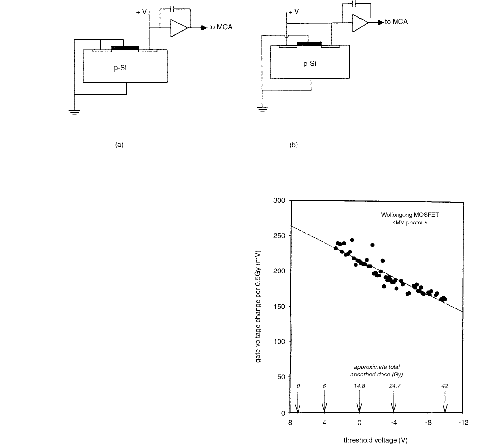
Figure 8.29 shows the reduction of dose response in the
Wollongong MOSFET, A, as a function of total gate voltage.
FIGURE 8.28 Connections for pulse-height measurement using the MOSFET (a) with only the drain connected to the PA and
(b) with source and drain both connected to the PA. (From Reference [16]. With permission.)
FIGURE 8.29 Variation of response with total absorbed dose
in MOSFET detector,
A, exposed to 4-MV photons from a med-
ical linear accelerator (Varian Clinac 600 C/4 MV). The change
required in gate voltage to compensate for the charge accumu-
lated due to 0.5 Gy absorbed dose was used as dose response.
It is shown as a function of total absorbed dose and the actual
MOSFET total gate voltage required to maintain a constant
current between source and drain. The bias applied during irra-
diation was 5 V. The broken line shows the best linear fit to the
experimental data (
r
2
0.877). (From Reference [17]. With
permission.)
Ch-08.fm Page 378 Friday, November 10, 2000 12:03 PM
Solid-State Dosimeters 379
The total gate voltage is related to the total absorbed dose
that is also indicated on the horizontal axis. The reduction
of dose response, expressed as gate voltage change per
absorbed dose, is a linear function of the total absorbed
dose. The detector response is reduced by approximately
3% for a gate voltage change of 1 V. This function was
used to correct the readings of the other Wollongong
MOSFET detectors.
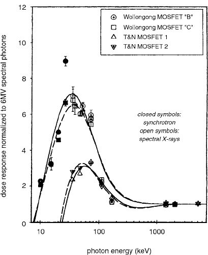
Figure 8.30 shows the variation of dose response with
photon energy relative to water for MOSFET detectors.
The two Wollongong-type detectors exhibit a maximum
of dose response relative to water around 35 keV. The
difference between the two detectors in the absolute dose
maximum of 7.1 and 6.5, respectively, approaches statis-
tical significance.
For comparison, the results obtained in spectral radia-
tion beams with the Thomson and Nielson [17] MOSFET
detectors are also plotted in Figure 8.30. The reduction of
dose response with total absorbed dose was found to be
less than 1% for a gate voltage change of 1 V, which is
considerably smaller than the one observed in the Wol-
longong MOSFETs. The dose response for different radi-
ation energies was corrected for this variation.
As can be seen in Figure 8.30, the Thomson and
Nielson detectors also exhibit a smaller variation of dose
response with photon energy, which is most likely due to
the use of a 2-mm resin on the detector. The over-response
was found to be on the order of a factor of 3, just above
an effective photon energy of 50 keV.
The sensitive element of a MOSFET detector is a
silicon oxide layer underneath the aluminum transistor
gate. The geometry of the sensing regions of the silicon
dioxide is slightly different for the two MOSFET devices
used by Rosenfeld et al. [18] In the case of the TOT500
p-MOSFET device, the gate oxide has a serpentine shape,
and in the case of the n-MOSFET device it was a rectan-
gular ribbon shape with an outer boundary dimension of
about 200 200
m
2
and a thickness of about 1
m for
both detectors.
The change in MOSFET threshold voltage, which is
proportional to the absorbed radiation dose, was measured
under constant current conditions. The n-channel MOSFET
chip was mounted inside a kovar package with the lid
removed. RADFET has a different topology than the
n-channel MOSFET and was mounted on a plastic board
under an epoxy bubble. Both MOSFET and RADFET
detectors were irradiated with a gale bias voltage of 5 V
to increase sensitivity and improve linearity of response.
The
n-MOSFET dosimeters were exposed in air, i.e.,
without any build-up material, to the microbeam in ‘‘normal’’
and ‘‘edge-on’’ orientations, and the p-MOSFET dosimeter
was placed in ‘‘edge-on’’ orientation only. The dose deliv-
ered to MOSFET per single irradiation shot in free-air
geometry was 17 monitor units (MU), which corresponds
to a maximum threshold voltage shift in the center of the
beam of about 150 mV. The results (Figure 8.31) prove that
the spatial resolution of a MOSFET dosimeter is indeed
affected by the orientation of the detector in the beam, the
resolution being superior for the ‘‘edge-on’’ mode. The
results demonstrate that the responses of
n-MOSFET and
RADFET in ‘‘edge-on’’ mode are almost independent of
package geometry and material for irradiation in free-air
geometry.
Electron fluence was calculated by Rosenfeld et al.
[19] from the dose measured in the water at a distance of
1 m from the virtual source. The fluence at the point of
irradiation was calculated using the inverse-square law.
The electron fluence and dose in Si was measured inde-
pendently using the Hamamatsu photodiode at the point
of irradiation from the relation
(8.8)
where,
I
d
photodiode current
w
Si
3.62 eV
t
ir
irradiation time
e 1.6 10
19
C
Si
density of Si
V
Si
sensitive volume of the photodiode (1 1
0.3 cm
3
).
A LINAC electron beam was used for monitoring of
the Hamamatsu photodiode response. The degradation of
FIGURE 8.30 Variation of the dose response with effective
radiation energy for MOSFET detector. The response is normal-
ized to 6-MV spectral x-rays. (From Reference [17]. With per-
mission.)
DSi()
I
d
w
Si
t
ir
e
Si
V
Si
----------------
Ch-08.fm Page 379 Friday, November 10, 2000 12:03 PM