Power electronic handbook
Подождите немного. Документ загружается.

438 S. Y. Hui and H. S. H. Chung
Circuits of Type 3–5 employ a switched mode front stage
circuit which pulls the dc link voltage to zero momentarily
whenever inverter switching is required. This soft-switching
approach does not cause extra voltage stress to the inverter
and hence the voltage rating of the power devices is only
1 per unit. As ZVS conditions can be created at any time,
there is virtually no restriction in the PWM strategies. There-
fore, well established PWM schemes developed in the last two
decades can be employed. In some ways, this approach is sim-
ilar to some dc-side commutation techniques proposed in the
past for thyristor inverters [46, 47], although these dc-side
commutation techniques were used for turning off thyristors
in the inverter bridge and were not primarily developed for
soft-switching.
Circuits of Type 6–8 retain the use of a constant dc link
voltage. They incorporate the use of the resonant components
and/or filter components into the inverter circuit operation.
This approach is particularly useful for inverter applications
in which output filters are required. Examples include unin-
terruptible power supplies (UPS) and inverters with output
filters for motor drives. The LC filter components can form
the auxiliary resonant circuits that create the soft-switching
conditions. However, these tend to have high power device
count and require complex control strategy.
V
S
L
C
S S
5
S
6
S
3
S
2
S
4
S
1
I
L
(a)
V
S
L
C
S
5
S
6
S
3
S
2
S
4
S
1
V
C
V
B
V
A
V
C
V
B
V
A
I
L
(b)
I
X
C
S
11
S
12
S
9
S
8
S
10
S
7
To
Load
(c)
L
S
5
S
6
S
3
S
2
S
4
S
1
3 phase
AC
C
r
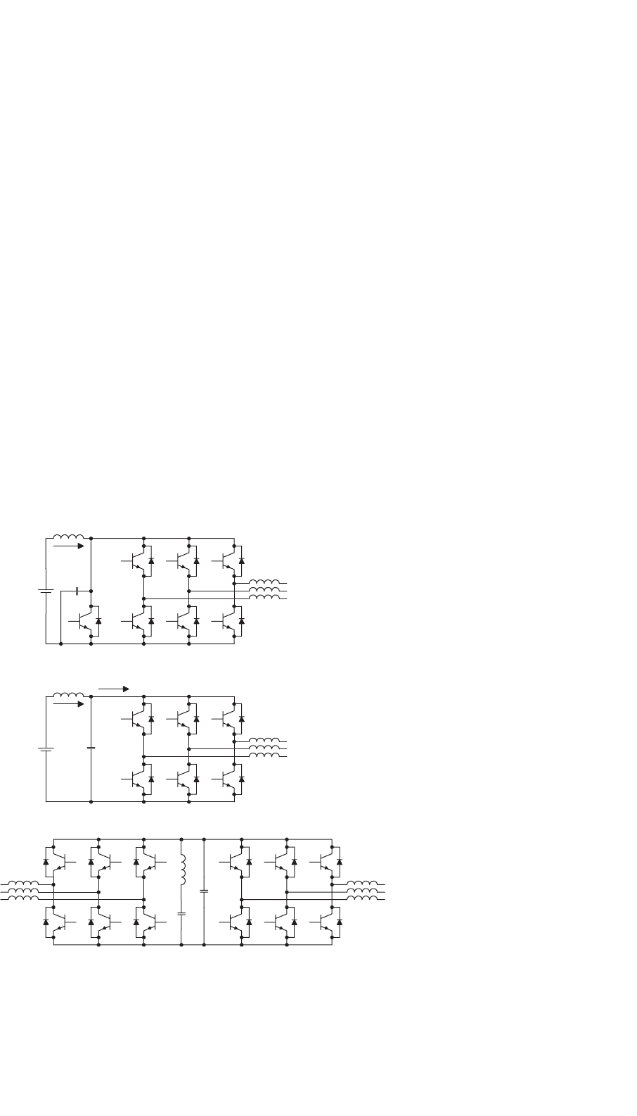
FIGURE 16.48 Resonant-link inverters.
16.14.1 Resonant (Pulsating) DC Link Inverter
Resonant DC link converter for DC–AC power conversion
was proposed in 1986 [42]. Instead of using a nominally con-
stant DC link voltage, a resonant circuit is added to cause
the DC link voltage to be pulsating at a high frequency.
This resonant circuit theoretically creates periodic zero-voltage
duration at which the inverter switches can be turned on or
off. Figure 16.48 shows the schematics of the pulsating link
inverter. Typical dc link voltage, inverter’s phase voltage and
the line voltages are shown in Fig. 16.49. Because the inverter
switching can only occur at zero voltage duration, integral
pulse density modulation (IPDM) has to be adopted in the
switching strategy.
Analysis of the resonant dc link converter can be simplified
by considering that the inverter system is highly inductive. The
equivalent circuit is shown in Fig. 16.50.
The link current I
x
may vary with the changing load condi-
tion, but can be considered constant during the short resonant
cycle. If switch S is turned on when the inductor current is I
Lo
,
the resonant dc link voltage can be expressed as
V
c
(
t
)
= V
s
+e
−αt
[
−V
s
cos
(
ωt
)
+ωLI
M
sin
(
ωt
)
]
(16.14)
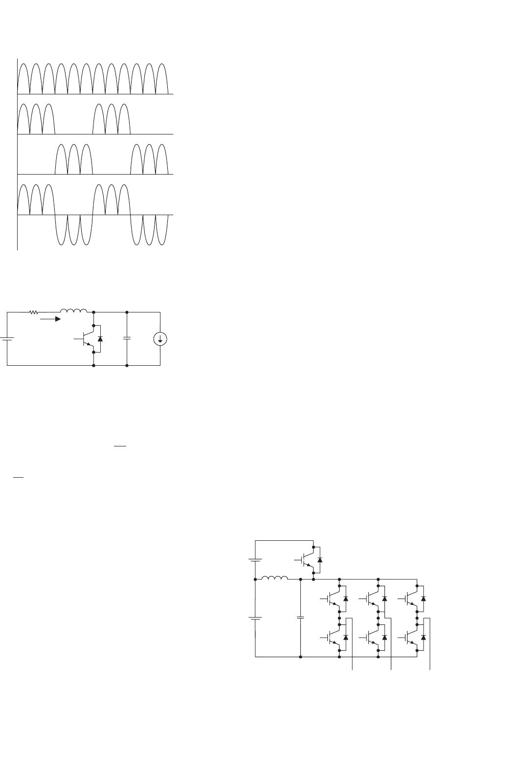
16 Resonant and Soft-switching Converters 439
V
0
V
A-B
V
B
V
A
FIGURE 16.49 Typical dc link voltage (V
0
), phase voltages (V
A
,V
B
),
and line voltage (V
AB
) of resonant link inverters.
V
S
R
L
+
V
C
−
S
I
X
I
L
FIGURE 16.50 Equivalent circuit of resonant link inverter.
and inductor current i
L
is
i
L
(
t
)
≈ I
x
+e
−αt
I
M
cos
(
ωt
)
+
V
s
ωL
sin
(
ωt
)
(16.15)
where α =
R
2L
(16.16)
ω
o
=
(
LC
)
−0.5
(16.17)
ω =
ω
2
o
−α
2
0.5
(16.18)
and I
M
= I
Lo
−I
x
(16.19)
The resistance in the inductor could affect the resonant
behavior because it dissipates some energy. In practice, (i
L
−I
x
)
has to be monitored when S is conducting. S can be turned
on when (i
L
− I
x
) equal to a desired value. The objective is to
ensure that the dc link voltage can be resonated to zero voltage
level in the next cycle.
The pulsating dc link inverter has the following advantages:
•
Reduction of switching loss.
• Snubberless operation.
• High switching frequency (> 18 kHz) operation becomes
possible, leading to the reduction of acoustic noise in
inverter equipment.
• Reduction of heatsink requirements and thus improve-
ment of power density.
This approach has the following limitations:
• The peak dc pulsating link voltage (2.0 per unit) is higher
than the nominal dc voltage value of a conventional
inverter. This implies that power devices and circuit com-
ponents of higher voltage ratings must be used. This
could be a serious drawback because power components
of higher voltage ratings are not only more expensive, but
usually have inferior switching performance than their
low-voltage counterparts.
•
Although voltage clamp can be used to reduce the peak
dc link voltage, the peak voltage value is still higher than
normal and the additional clamping circuit makes the
control more complicated.
• Integral pulse-density modulation has to be used. Many
well-established PWM techniques cannot be employed.
Despite these advantages, this resonant converter concept
has paved the way for other soft-switched converters to
develop.
16.14.2 Active-clamped Resonant DC Link
Inverter
In order to solve the high voltage requirement in the basic pul-
sating dc link inverters, active clamping techniques (Fig. 16.51)
have been proposed. The active clamp can reduce the per-
unit peak voltage from 2.0 to about 1.3–1.5 [44]. It has been
reported that operating frequency in the range of 60–100 kHz
has been achieved [48] with an energy efficiency of 97% for a
50 kVA drive system.
V
dc
L
r
C
r
V
cc
FIGURE 16.51 Active-clamp resonant link inverter.
440 S. Y. Hui and H. S. H. Chung
The design equations for active-clamped resonant link
inverter are
T
L
=
1
f
L
=2
L
r
C
r
cos
−1
1−k
+
k
2−k
k −1
(16.20)
where T
L
is the minimum link period, f
L
is the maximum link
frequency, and k is the clamping ratio. For the active-clamped
resonant inverter, k is typically 1.3–1.4 per unit.
The rate of rise of the current in the clamping device is
di
dt
=
k − 1
V
s
L
r
(16.21)
The peak clamping current required to ensure that the dc bus
return to zero volt is
I
sp
= V
s
k
2 −k
C
r
L
r
(16.22)
In summary, resonant (pulsating) dc link inverters offer
significant advantages such as:
• High switching frequency operation.
• Low dv/dt for power devices.
• ZVS with reduced switching loss.
• Suitable for 1–250 kW.
• Rugged operation with few failure mode.
16.14.3 Resonant DC Link Inverter with Low
Voltage Stress [49]
A resonant dc link inverter with low voltage stress is shown in
Fig. 16.52. It consists of a front-end resonant converter that can
pull the dc link voltage down just before any inverter switching.
This resonant dc circuit serves as an interface between the dc
power supply and the inverter. It essentially retains all the
C
r
L
r
T
1
C
dc
T
3
T
2
D
1
L
dc
I.M.
FIGURE 16.52 Resonant DC link inverter with low voltage stress.
advantages of the resonant (pulsating) dc link inverters. But it
offers extra advantages such as:
• No increase in the dc link voltage when compared with
conventional hard-switched inverter. That is, the dc link
voltage is 1.0 per unit.
• The zero voltage condition can be created at any time.
The ZVS is not restricted to the periodic zero-voltage
instants as in resonant dc link inverter.
• Well-established PWM techniques can be employed.
• Power devices of standard voltage ratings can be used.
The timing program and the six operating modes of this
resonant circuit are as shown in Figs. 16.53 and 16.54,
respectively.
I
Lr
V
C
r
t
V
S
I
3
I
on
I
2
I
1
I
0
t
5
t
4
t
3
t
2
t
1
t
0
M1 M2 M3 M4 M5
FIGURE 16.53 Timing diagram of resonant link inverter with mini-
mum voltage stress.
(1) Normal mode:
This is the standard PWM inverter mode. The resonant
inductor current i
Lr
(t) and the resonant voltage V
cr
(t) are
given by
i
Lr
(
t
)
= 0
v
Cr
(
t
)
= V
s
where V
s
is the nominal dc link voltage.
16 Resonant and Soft-switching Converters 441
C
r
L
r
T
1
C
dc
T
3
T
2
D
2
D
1
L
dc
I
o
V
dc
(b) mode 1
C
r
L
r
T
1
C
dc
T
3
T
2
D
2
D
1
L
dc
I
o
V
dc
(a) normal mode
C
r
L
r
T
1
C
dc
T
3
T
2
D
2
D
1
L
dc
I
o
V
dc
(c) mode 2
C
r
L
r
T
1
C
dc
T
3
T
2
D
2
D
1
L
dc
I
o
V
dc
(d) mode 3
C
r
L
r
T
1
C
dc
T
3
T
2
D
2
D
1
L
dc
I
o
V
dc
(e) mode 4
C
r
L
r
T
1
C
dc
T
3
T
2
D
2
D
1
L
dc
I
o
V
dc
(f) mode 5
FIGURE 16.54 Operating modes of resonant link inverter with minimum voltage stress.
(2) Mode 1 (initiating mode): (t
0
−t
1
)
At t
0
, mode 1 begins by switching on T2 and T3 on with
zero current. i
Lr
(t) increases linearly with a di/dt of V
s
/L
r
.If
i
Lr
(t) is equal to the initialized current I
i
, T1 is zero-voltage
turned off. If (I
s
−I
o
) < I
i
, then the initialization is ended
when i
Lr
(t) is equal to I
i
, where I
s
is the current flowing
into the dc inductor L
dc
.If(I
s
−I
o
) > I
i
, then this mode
continues until i
Lr
(t) is equal to (I
s
−I
o
). The equations in
this interval are
i
Lr
(
t
)
=
V
s
L
r
t
v
Cr
(
t
)
= V
s
i
Lr
(
t
1
)
=
V
s
L
r
t
1
= I
i
(3) Mode 2 (Resonant mode): (t
1
−t
2
)
After T1 is turned off under ZVS condition, resonance
between L
r
and C
r
occurs. V
cr
(t) decreases from V
s
to 0.
At t
2
, i
Lr
(t) reaches the peak value in this interval. The
equations are:
i
Lr
(
t
)
=
V
s
Z
r
sin
(
ω
r
t
)
+
[
I
1
+
(
I
o
−I
s
)
]
cos
(
ω
r
t
)
−
(
I
o
−I
s
)
V
Cr
(
t
)
=−V
s
cos
(
ω
r
t
)
−
[
I
1
+
(
I
o
−I
s
)
]
Z
r
sin
(
ω
r
t
)
i
Lr
(
t
2
)
= I
2
= I
Lr,peak
V
Cr
(
t
2
)
= 0
where
Z
r
=
L
r
C
r
and ω
r
=
1
√
L
r
C
r
442 S. Y. Hui and H. S. H. Chung
(4) Mode 3 (Freewheeling mode): (t
2
−t
3
)
The resonant inductor current flows through two freewheel-
ing paths (T2-Lr-D2 and T3-D1-Lr). This duration is the zero
voltage period created for ZVS of the inverter, and should be
longer than the minimum on and off times of the inverter’s
power switches.
i
Lr
(
t
)
= I
2
v
Cr
(
t
)
= 0
(5) Mode 4 (Resonant mode): (t
3
−t
4
)
This mode begins when T2 and T3 are switched off under
ZVS. The second half of the resonance between L
r
and C
r
starts again. The capacitor voltage V
cr
(t) increases back from
0toV
s
and is clamped to V
s
. The relevant equations in this
mode are
i
Lr
(
t
)
=
[
I
2
−
(
I
on
−I
s
)
]
cos
(
ω
r
t
)
−
(
I
on
−I
s
)
V
Cr
(
t
)
=
[
I
2
−
(
I
on
−I
s
)
]
Z
r
sin
(
ω
r
t
)
i
Lr
(
t
4
)
= I
3
V
Cr
(
t
4
)
= V
s
where I
on
is the load current after the switching state.
(6) Mode 5 (Discharging mode): (t
4
−t
5
)
In this period, T1 is switched on under ZV condition because
V
cr
(t) = V
s
. The inductor current decreases linearly. This
mode finishes when i
Lr
(t) becomes zero.
i
Lr
(
t
)
=−
V
s
L
r
t +I
3
v
Cr
(
t
)
= V
s
i
Lr
(
t
5
)
= 0
16.14.4 Quasi-resonant Soft-switched
Inverter [50]
(A) Circuit Operation
Consider an inverter fed by a dc voltage source vs a front-stage
interface circuit shown in Fig. 16.55, can be added between the
dc voltage source and the inverter. The front-stage circuit con-
sists of a quasi-resonant circuit in which the first half of the
resonance cycle is set to occur to create the zero-voltage con-
dition whenever inverter switching is needed. After inverter
switching has been completed, the second half of the reso-
nance cycle takes place so that the dc link voltage is set back to
its normal level. To avoid excessive losses in the resonant cir-
cuit, a small capacitor C
r1
is normally used to provide the dc
link voltage whilst the large smoothing dc link capacitor C
1
is
isolated from the resonant circuit just before the zero-voltage
DC
source
L
s
S
b
C
1
S
r1
S
r2
C
r2
C
r1
L
r
to
inverter
D
b
+
−
FIGURE 16.55 Quasi-resonant circuit for soft-switched inverter.
300
−200
−100
0
100
200
t
0
t
5
t
4
t
3
t
2
t
1
V
cr1
V
cr2
Time
Voltage(V)
FIGURE 16.56 Typical waveforms for V
cr1
and V
cr2
.
duration. This method avoids the requirement for pulling the
dc voltage of the bulk capacitor to zero.
The period for this mode is from t
0
to t
1
in Fig. 16.56. In this
mode, switch S
b
is turned on and switches S
r1
and S
r2
are
turned off. The inverter in Fig. 16.55 works like a conventional
dc link inverter. In this mode, V
cr1
= V
c1
. The voltage across
switch S
b
is zero. Before an inverter switching takes place, when
switch S
r1
is triggered at t
1
to discharge C
r1
. This operating
mode ends at t
2
when V
cr1
approaches zero. The equivalent
circuit in this mode is shown in Fig. 16.57a. The switch S
b
must
be turned off at zero voltage when switch S
r1
is triggered. After
S
r1
is triggered, C
r1
will be discharged via the loop C
r1
, C
r2
, L
r
,
and S
r1
. Under conditions of V
cr2
≤ 0 and C
r1
≤ C
r2
, the
energy stored in C
r1
will be transferred to C
r2
and V
cr1
falls to
zero in the first half of the resonant cycle in the equivalent
circuit of Fig. 16.57a. V
cr1
will be clamped to zero by the
freewheel diodes in the inverter bridge and will not become
negative. Thus, V
cr1
can be pulled down to zero for zero-
voltage switching. When the current in inductor L
r
becomes
zero, switch S
r1
can be turned off at zero current.
Inverter switching can take place in the period from t
2
to
t
3
in which V
cr1
remains zero. This period must be longer
than the turn-on and turn-off times of the switches. When
inverter switching has been completed, it is necessary to reset
the voltage of capacitor C
r1
. The equivalent circuit in this
mode is shown in Fig. 16.57b. The current in inductor L
r
reaches zero at t
3
. Due to the voltage in V
cr2
and the presence
16 Resonant and Soft-switching Converters 443
Vs
L
s
L
r
S
r1
C
r1
I
o
D
r
(a) Mode 2
C
r2
Vs
L
s
L
r
S
r1
C
r1
I
o
D
r
(b) Mode 4
C
r2
Vs
L
s
L
r
S
r2
I
o
(c) Mode 5
C
r2
FIGURE 16.57 Equivalent circuits of the quasi-resonant circuit for
different modes.
of diode D
r
, this current then flows in the opposite direction.
C
r1
will be recharged via L
r
, C
r2
, C
r1
, and D
r
. The diode D
r
turns off when the current in L
r
becomes zero. V
cr1
will not
go beyond 1 per unit because C
r1
is clamped to supply volt-
age by diode D
b
. The switch S
b
can be turned on again at
zero-voltage condition when V
cr1
returns to normal dc supply
voltage. After D
r
turns off, V
cr2
may not be zero. Some pos-
itive residual capacitor voltage remains in C
2
at t
4
, as shown
in Fig. 16.56. In case V
cr2
is positive, V
cr1
cannot be pulled
down to zero again in the next switching cycle. Therefore,
S
r2
should be triggered after t
4
to reverse the residual volt-
age in C
r2
. At time t
5
,Sr
2
turns off at zero-current condition
and V
cr2
is now reversed to negative. The equivalent circuit
in this mode is shown in Fig. 16.57c. When V
cr2
≤ 0 and
C
r1
≤ C
r2
, V
cr1
can be pulled down to zero again before the
next inverter switching. The operation can then be repeated in
next switching cycle.
(B) Design Considerations
(1) C
r1
and C
r2
The criterion for getting zero capacitor voltages V
cr1
is:
(C
r1
−C
r2
)V
s
+2C
r2
V
o2
−Iπ
L
r
C
e
≤ 0 (16.23)
where
• V
o1
is the initial voltage of C
r1
;
• V
o2
is the initial voltage of C
r2
;
• i
L0
is the initial current of inductor L
r
;
• I = I
o
−I
s
, which is the difference between load current
and supply current. It is assumed to be a constant within
a resonant cycle;
• R
r
is the equivalent resistance in the resonant circuit.
• C
e
=
C
r1
C
r2
C
r1
+C
r2
When I ≥ 0, the above criterion is always true under
conditions of:
C
r1
≤ C
r2
, V
o2
≤ 0
The criterion for recharging voltage V
cr1
to 1 per unit dc link
voltage is:
2C
r2
C
r1
+C
r2
V
o2
−
I
C
r1
+C
r2
π
L
r
C
e
≥ V
s
(16.24)
(2) Inductor L
r
The inductor L
r
should be small so that the dc link voltage can
be decreased to zero quickly. However, a small L
r
could result
in large peak resonant current and therefore requirement of
power devices with large current pulse ratings. An increase in
the inductance of L
r
can limit the peak current in the quasi-
resonant circuit. Because the resonant frequency depends on
both the inductor and the capacitor, therefore, the selection
of L
r
can be considered together with the capacitors C
r1
and
C
r2
and with other factors such as the current ratings of power
devices, the zero-voltage duration and the switching frequency
required in the soft-switching circuit.
(3) Triggering instants of the switches
The correct triggering instants for the switches are essential
for the successful operation of this soft-switched inverter. For
the inverter switches, the triggering instants are determined
from a PWM modulation. Let T
s
be the time at which the
inverter switches change states. To get the zero-voltage inverter
switching, switch S
r1
should be turned on half resonant cycle
before the inverter switching instant. The turn-on instant of
S
r1
, which is t
1
in Fig. 16.56, can be written as:
t
1
= T
s
−
π
ω
(16.25)
where ω =
ω
2
0
−α
2
, α =
R
r
2L
r
, ω
0
=
1
L
r
C
e
. The switch S
b
is turned off at t
1
.
444 S. Y. Hui and H. S. H. Chung
S
r1
may be turned off during its zero current period when
diode D
r
is conducting. For easy implementation, its turn-off
time can be selected as T
s
+ π/ω. Because the dc link voltage
can be pulled down to zero in less than half resonant cycle,
T
s
should occur between t
2
and t
3
.
At time t
3
(the exact instant depends on the I), the diode
D
r
turns on in the second half of the resonant cycle to recharge
C
r1
.Att
4
, V
cr1
reaches 1 per unit and diode D
b
clamps V
cr1
to
1 per unit. The switch S
b
can be turned on again at t
4
, which
is half resonant cycle after the start of t
3
:
t
4
≈ t
3
+
π
ω
(16.26)
As t
3
cannot be determined accurately, a voltage sensor in
principle can be used to provide information for t
4
so that S
b
can be turned on to reconnect C
1
to the inverter. In practice,
however, S
b
can be turned on a few microseconds (longer than
T
s
+π/ω) after t
2
without using a voltage sensor (because it is
not critical for S
b
to be on exactly at the moment V
cr
reaches
the nominal voltage). As for switch S
r2
, it can be turned on a
few microseconds after t
4
. It will be turned off half of resonant
cycle (π
√
L
r
C
r2
)intheL
r
−C
r2
circuit later. In practice, the
timing of S
r1
,S
r2
, and S
b
can be adjusted in a simple tuning
procedure for a given set of parameters. Figure 16.58 shows
the measured gating signals of S
r1
,S
r2
, and S
b
with the dc link
voltage V
cr1
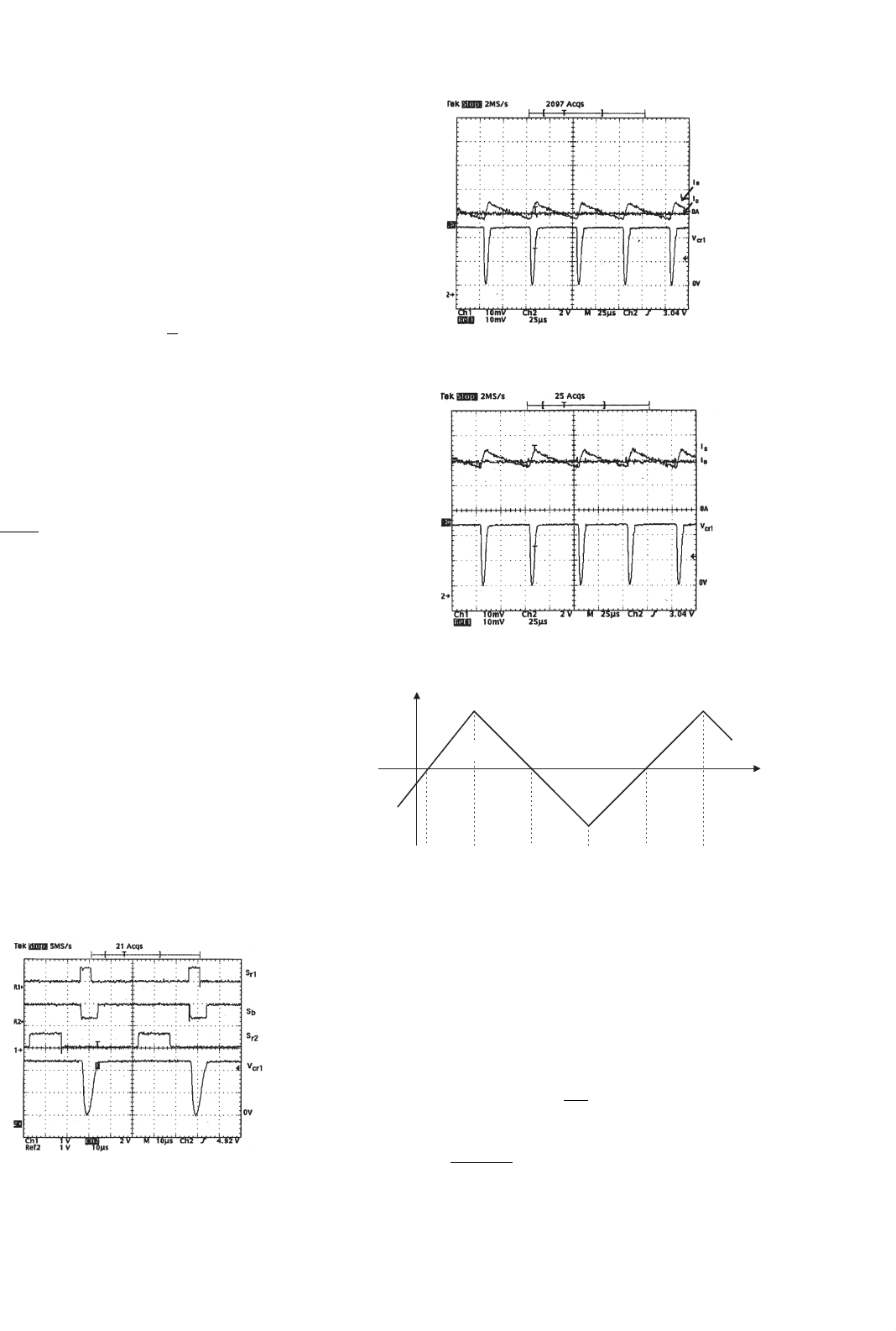
in a 20 kHz switching inverter. Figures 16.59 and
16.60 show the measured waveforms of I
s
, I
o
, and V
cr1
under
no load condition and loaded condition, respectively.
(C) Control of Quasi-resonant Soft-switched Inverter Using
Digital Time Control (DTC) [51]
Based on the zero-average-current error (ZACE) control con-
cept, a digital time control method has been developed for a
current-controlled quasi-resonant soft-switched inverter. The
basic ZACE concept is shown in Fig. 16.61. The current error
is obtained from the difference of a reference current and the
sensed current. The idea is to make the areas of each transition
(A1 and A2) equal. If the switching frequency is significantly
greater than the fundamental frequency of the reference signal,
FIGURE 16.58 Gating signals for S
r1
,S
r2
, and S
b
with V
cr1
.
FIGURE 16.59 Typical I
s
, I
o
, and V
cr1
under no-load condition.
FIGURE 16.60 Typical I
s
, I
o
, and V
cr1
under loaded condition.
time, s
error
current,
A
t
n
t
n+1
t
n+5
t
n+4
t
n+3
t
n+2
A
1
A
2
FIGURE 16.61 Zero-average-current error (ZACE) control concept.
the rising and falling current segments can be assumed to be
linear. The following simplified equation can be established.
t
n+1
= t
n+1
−t
n
(16.27)
The control algorithm for the inverter is
t
n+3
= t
n+2
+D
T
sw
2
−
(
t
n+2
−t
n
)
(16.28)
where D =
t
n+2
t
n+2
−t
n
and T
sw
= t
n+4
−t
n
.
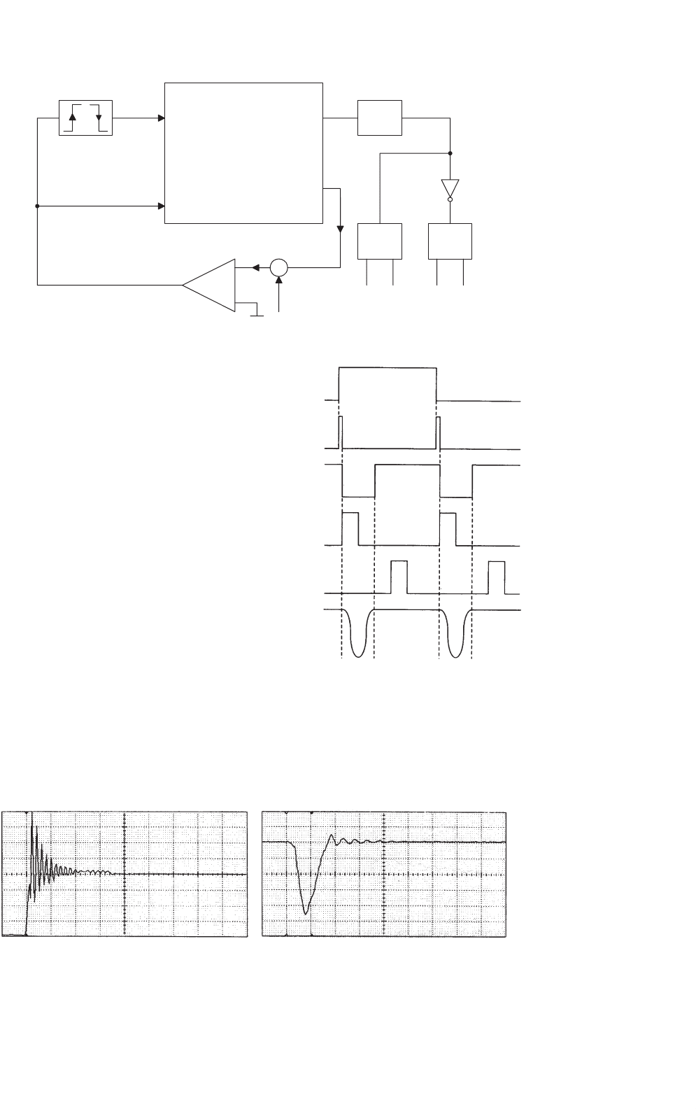
16 Resonant and Soft-switching Converters 445
QRC
delay
turn-on
delay
turn-on
delay
Σ
IRQ
edge
edge
detector
−
+
i
err
i
sign
i
ref
Q
comparator
current
error
hi/lo detect
reference
sine wave
switch
control
digital signal
processor AD-2181
S
1
sensed
output
current
I
O
S
2
S
3
S
4
interrupt
−
+
FIGURE 16.62 Implementation of DTC.
The schematic of a digital signal processor (DSP) based
controller for the DTC method is shown in Fig. 16.62. The
duty cycle can be approximated from the reference sine wave
by level shifting and scaling it between 0 and 1. The time
t
n+2
– t
n
is the sum of t
n+1
and t
n+2
. These data pro-
vide information for the calculation of the next switching time
t
n+1
.
The switches are triggered by the changing edge of the switch
control Q. Approximate delays are added to the individual
switching signals for both the inverter switches and the quasi-
resonant switches. Typical gating waveforms are shown in
Fig. 16.63. The use of the quasi-resonant soft-switched inverter
is a very effective way in suppressing switching transient and
EMI emission. Figures 16.64a,b show the inverter switch volt-
age waveforms of a standard hard-switched inverter and a
quasi-resonant soft-switched inverter, respectively. It is clear
that the soft-switched waveform has much less transient than
the hard-switched waveform.
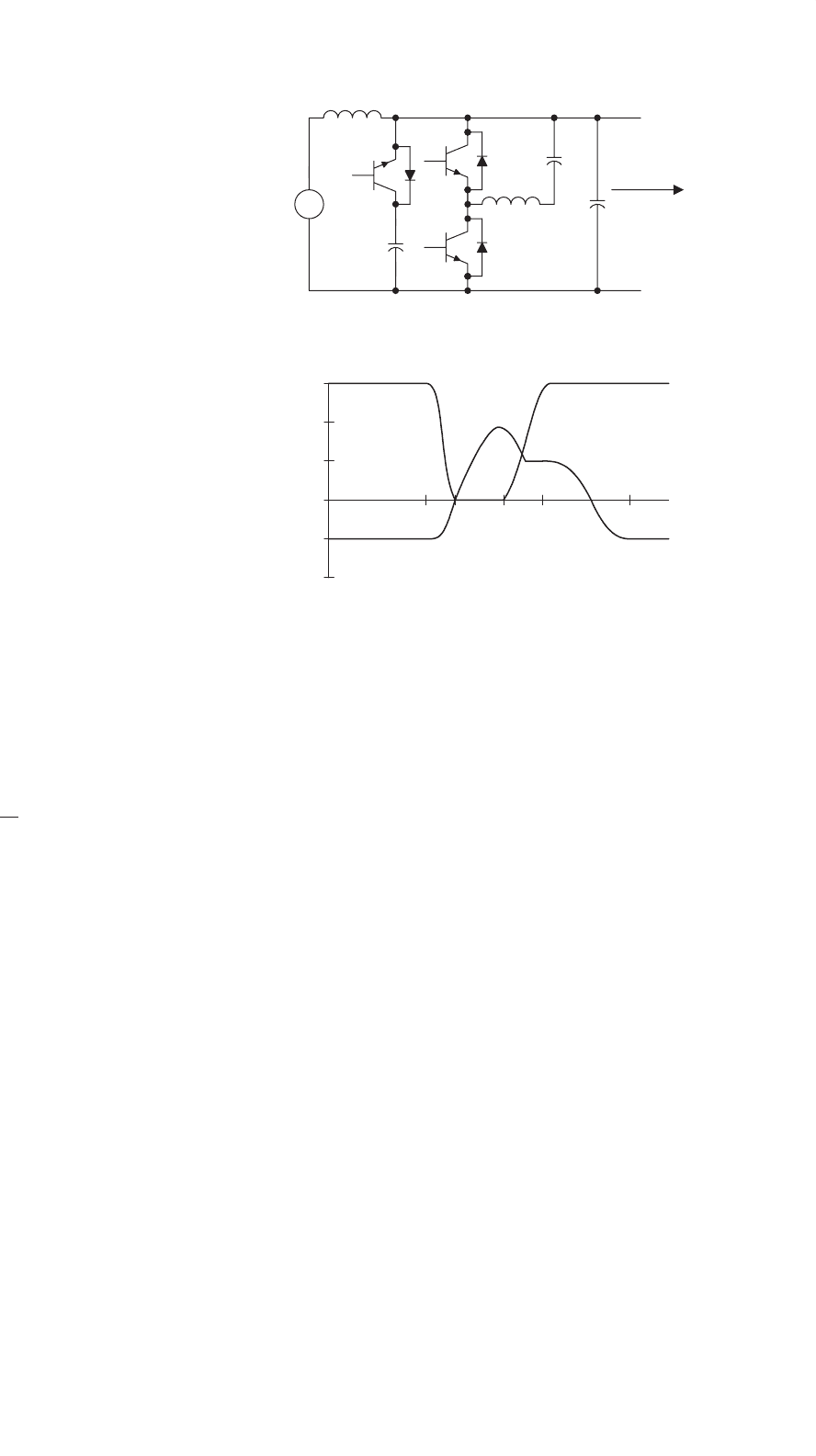
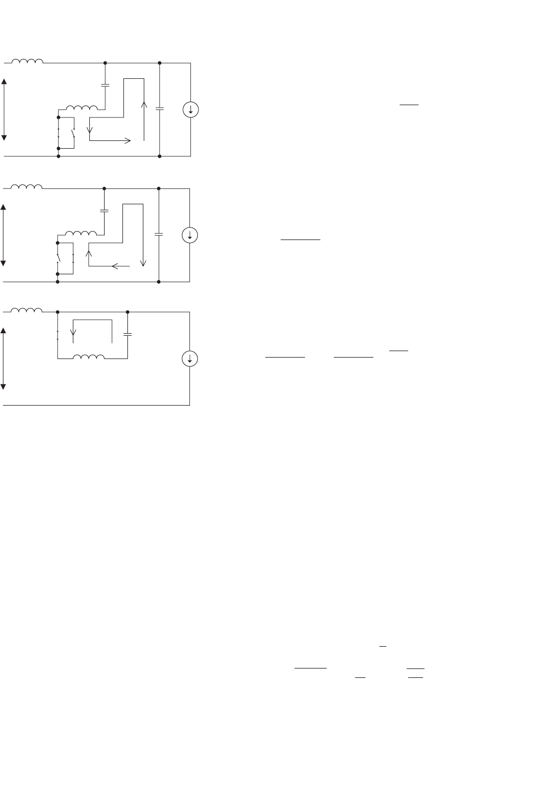
16.14.5 Resonant Pole Inverter (RPI) and
Auxiliary Resonant Commutated Pole
Inverter (ARCPI)
The resonant pole inverter integrates the resonant compo-
nents with the output filter components L
f
and C
f
. The load
(a) (b)
FIGURE 16.64 (a) Typical switch voltage under hard turn-off and (b) typical switch voltage under soft turn-off.
Q
edge
detect
S
b
S
r1
S
r2
voltage
across C
r1
FIGURE 16.63 Timing diagrams for the gating signals.
446 S. Y. Hui and H. S. H. Chung
T
1
D
1
C
r/2
C
f/2
L
f
=L
r
T
2
D
2
C
r/2
C
f/2
Load
I
f
=I
r
V
o
+
V
dc
−
V
f
FIGURE 16.65 One leg of a resonant pole inverter.
T
1
D
1
C
1
C
f
L
f
=L
r
T
2
D
2
C
2
Ir
I
o
T
3
D
3
C
3
T
4
D
4
C
4
V
o
FIGURE 16.66 Single-phase resonant pole inverter.
is connected to the mid-point of the dc bus capacitors as
shown in Fig. 16.65. It should however be noted that the RPI
can be described as a resonant inverter. Figure 16.66 shows a
single-phase RPI. Its operation can be described with the tim-
ing diagram in Fig. 16.67. The operating modes are included
in Fig. 16.68. The RPI provides soft-switching for all power
switches. But it has two disadvantages. First, the power devices
have to be switched continuously at the resonant frequency
T
2
T
3
T
2
T
3
D
2
D
3
C
x
T
1
T
4
D
1
D
4
C
x
C
x
=C
1
,C
2
,C
3
,C
4
=C
r/2
t
t
I
f
V
f
V
dc
I
o
I
r
peak
FIGURE 16.67 Timing diagram for a single-phase resonant pole inverter.
determined by the resonant components. Second, the power
devices in the RPI circuit require a 2.2–2.5 p.u. current turn-off
capability.
An improved version of the RPI is the auxiliary reso-
nant commutated pole inverter (ARCPI). The ARCPI for one
inverter leg is shown in Fig. 16.69. Unlike the basic RPI, the
ARCPI allows the switching frequency to be controlled. Each of
the primary switches is closely paralleled with a snubber capac-
itor to ensure ZV turn off. Auxiliary switches are connected
in series with an inductor, ensuring that they operate under
ZC conditions. For each leg, an auxiliary circuit comprising
two extra switches A1 and A2, two freewheeling diodes, and a
resonant inductor L
r
is required. This doubles the number of
power switches when compared with hard-switched inverters.
Figure 16.70 shows the three-phase ARCPI system. Depending
on the load conditions, three commutation modes are gen-
erally needed. The commutation methods at low and high
current are different. This makes the control of the ARCPI
very complex. The increase in control and circuit complexity
represents a considerable cost penalty [52, 53].
16 Resonant and Soft-switching Converters 447
T
1
C
2
L
r
=L
f
C
f
R
C
3
T
4
+−
I
o
I
f
=I
r
+
V
dc
−
(a)
C
1
D
2
L
f
C
f
R
D
3
C
4
I
o
I
f
+
V
dc
−
(b)
(c)
C
1
T
2
L
f
C
f
R
T
3
C
4
I
o
+ V
o
−
+ V
o
−
I
f
+
V
dc
−
D
1
C
2
L
f
C
f
R
C
3
D
4
I
o
I
f
+
V
dc
−
(d)
+ V
o
−
+ V
o
−
V
f
FIGURE 16.68 Operating modes of a single-phase resonant pole inverter.
2C
dc
L
r
L
F
D
1
C
r/2
2C
dc
D
2
C
r/2
I
F
V
F
+
V
dc
−
I
r
p-channel
MCT
A
2
A
1
FIGURE 16.69 Improved resonant pole inverter leg.
2C
dc
L
r
2C
dc
+
V
dc
−
V
o3
L
F
2
AC AC AC
C
F2
L
F1a
C
F1
I
o3
V
o2
L
F2
C
F2
I
o2
V
o1
L
F2
C
F2
I
o1
3 phase load
AC
L
F1b
V
i
L
F1a
C
F1
L
F1b
V
i
L
F1a
C
F1
L
F1b
V
i
AC
Auxiliary Circuit (AC)
RECTIFIER INVERTER
A2A1
FIGURE 16.70 Three-phase auxiliary resonant commutated pole inverter (ARCPI).