Power electronic handbook
Подождите немного. Документ загружается.

408 S. Y. Hui and H. S. H. Chung
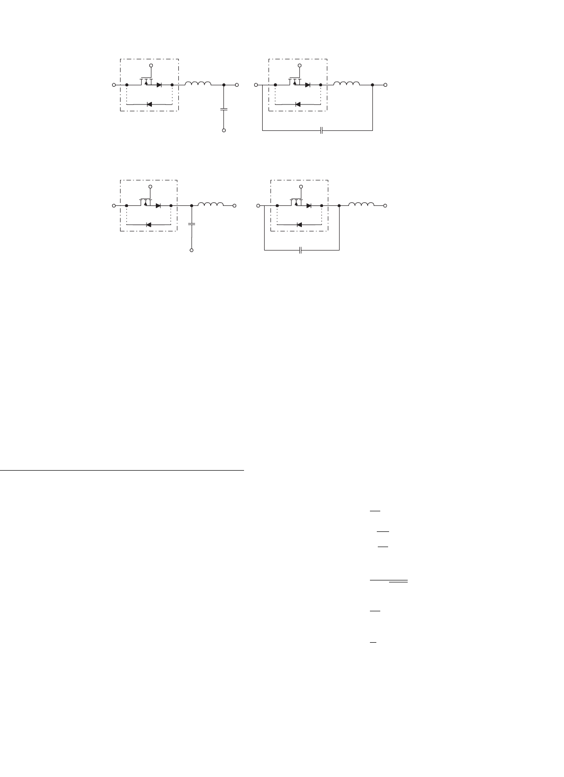
L
r
C
r
S
(a)
L
r
C
r
S
(b)
FIGURE 16.3 Zero-current (ZC) resonant switch.
L
r
S
(a)
C
r
L
r
C
r
S
(b)
FIGURE 16.4 Zero-voltage (ZV) resonant switch.
If the switch S is a unidirectional switch, the voltage across the
capacitor C
r
can oscillate freely in both positive and negative
half-cycle. Thus, the resonant switch can operate in full-wave
mode. If a diode is connected in anti-parallel with the unidi-
rectional switch, the resonant capacitor voltage is clamped by
the diode to zero during the negative half-cycle. The resonant
switch will then operate in half-wave mode. The objective of a
ZV switch is to use the resonant circuit to shape the switch
voltage waveform during the off time in order to create a
zero-voltage condition for the switch to turn on [13].
16.4 Quasi-resonant Converters
Quasi-resonant converters (QRCs) can be considered as a
hybrid of resonant and PWM converters. The underlying prin-
ciple is to replace the power switch in PWM converters with
the resonant switch. A large family of conventional converter
circuits can be transformed into their resonant converter coun-
terparts. The switch current and/or voltage waveforms are
forced to oscillate in a quasi-sinusoidal manner, so that ZCS
and/or ZVS can be achieved. Both ZCS-QRCs and ZVS-QRCs
have half-wave and full-wave mode of operations [8–10, 12].
16.4.1 ZCS-QRCs
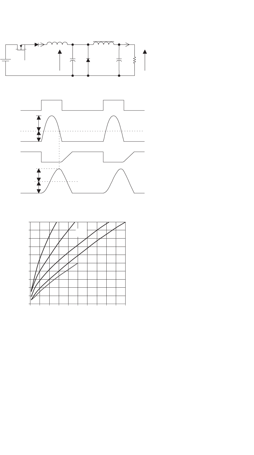
A ZCS-QRC designed for half-wave operation is illustrated
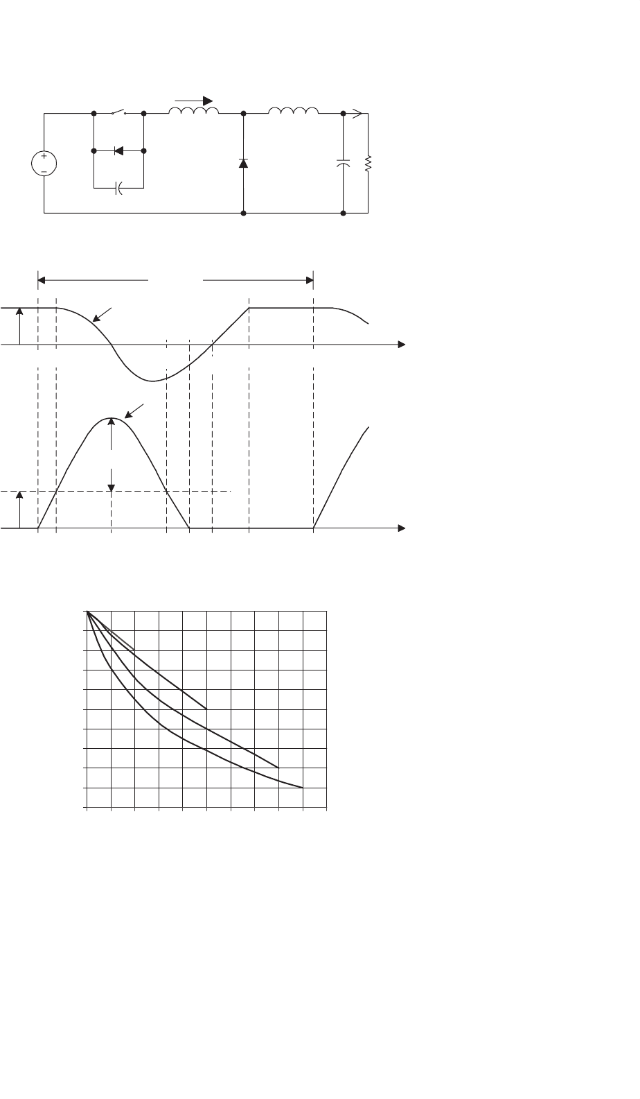
with a buck type DC–DC converter. The schematic is shown
in Fig. 16.5a. It is formed by replacing the power switch in con-
ventional PWM buck converter with the ZC resonant switch in
Fig. 16.3a. The circuit waveforms in steady state are shown in
Fig. 16.5b. The output filter inductor L
f
is sufficiently large so
that its current is approximately constant. Prior to turning the
switch on, the output current I
o
freewheels through the out-
put diode D
f
. The resonant capacitor voltage V
Cr
equals zero.
At t
0
, the switch is turned on with ZCS. A quasi-sinusoidal
current I
S
flows through L
r
and C
r
, the output filter, and
the load. S is then softly commutated at t
1
with ZCS again.
During and after the gate pulse, the resonant capacitor volt-
age V
Cr
rises and then decays at a rate depending on the
output current. Output voltage regulation is achieved by con-
trolling the switching frequency. Operation and characteristics
of the converter depend mainly on the design of the resonant
circuit L
r
C
r
. The following parameters are defined: voltage
conversion ratio M, characteristic impedance Z
r
, resonant fre-
quency f
r
, normalized load resistance r, normalized switching
frequency γ.
M =
V
o
V
i
(16.1a)
Z
r
=
L
r
C
r
(16.1b)
f
r
=
1
2π
√
L
r
C
r
(16.1c)
r =
R
L
Z
r
(16.1d)
γ =
f
s
f
r
(16.1e)
It can be seen from the waveforms that if I
o
> V
i
/Z
r
, I
S
will
not come back to zero naturally and the switch will have to be
16 Resonant and Soft-switching Converters 409
V
i
S CR1
D
f
L
r
L
f
C
r
C
f
R
L
V
o
V
Cr
I
o
i
Lr
(a)
gate signal
to S
I
Lr
V
DS
V
Cr
Tt
1
t
0
V
i
/Z
r
I
o
V
i
V
i
(b)
0
0.1
0.2
0.3
0.4
0.5
0.6
0.7
0.8
0.9
1
0 0.1 0.2 0.3 0.4 0.5 0.6 0.7 0.8
0.9
1
γ
M
0.5
1
r =2
5
10
(c)
FIGURE 16.5 Half-wave, quasi-resonant buck converter with ZCS: (a) schematic diagram; (b) circuit waveforms; and (c) relationship between
M and γ.
forced off, thus resulting in turn-off losses. The relationships
between M and γ at different r are shown in Fig. 16.5c. It can
be seen that M is sensitive to the load variation. At light load
conditions, the unused energy is stored in C
r
, leading to an
increase in the output voltage. Thus, the switching frequency
has to be controlled, in order to regulate the output voltage.
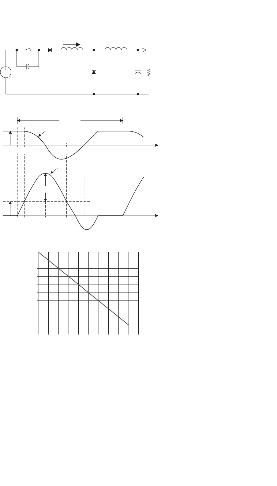
If an anti-parallel diode is connected across the switch,
the converter will be operating in full-wave mode. The cir-
cuit schematic is shown in Fig. 16.6a. The circuit waveforms
in steady state are shown in Fig. 16.6b. The operation is
similar to the one in half-wave mode. However, the induc-
tor current is allowed to reverse through the anti-parallel
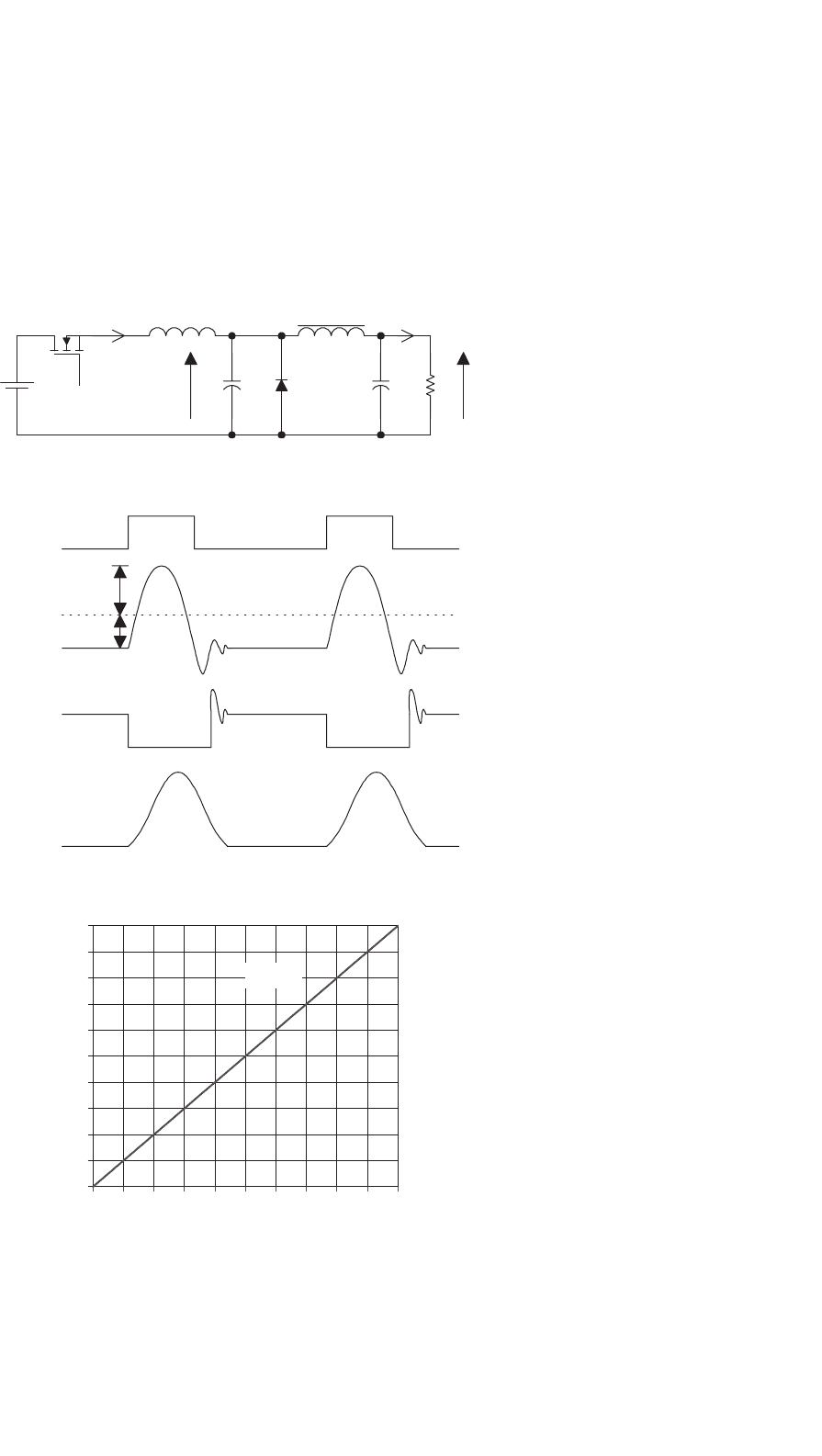
410 S. Y. Hui and H. S. H. Chung
diode and the duration for the resonant stage is lengthened.
This permits excess energy in the resonant circuit at light
loads to be transferred back to the voltage source V
i
. This
significantly reduces the dependence of V
o
on the output load.
The relationships between M and γ at different r are shown
in Fig. 16.6c. It can be seen that M is insensitive to load
variation.
V
i
S
D
f
L
r
L
f
C
r
C
f
R
L
i
Lr
V
o
V
Cr
I
o
(a)
V
DS
Tt
0
gate signal
to S
I
Lr
V
Cr
t
1
V
i
/Z
r
I
o
(b)
γ
M
r =1−10
(c)
0
0.1
0.2
0.3
0.4
0.5
0.6
0.7
0.8
0.9
1
0 0.1 0.2 0.3 0.4 0.5 0.6 0.7 0.8
0.9
1
FIGURE 16.6 Full-wave, quasi-resonant buck converter with ZCS: (a) schematic diagram; (b) circuit waveforms; and (c) relationship between
M and γ.
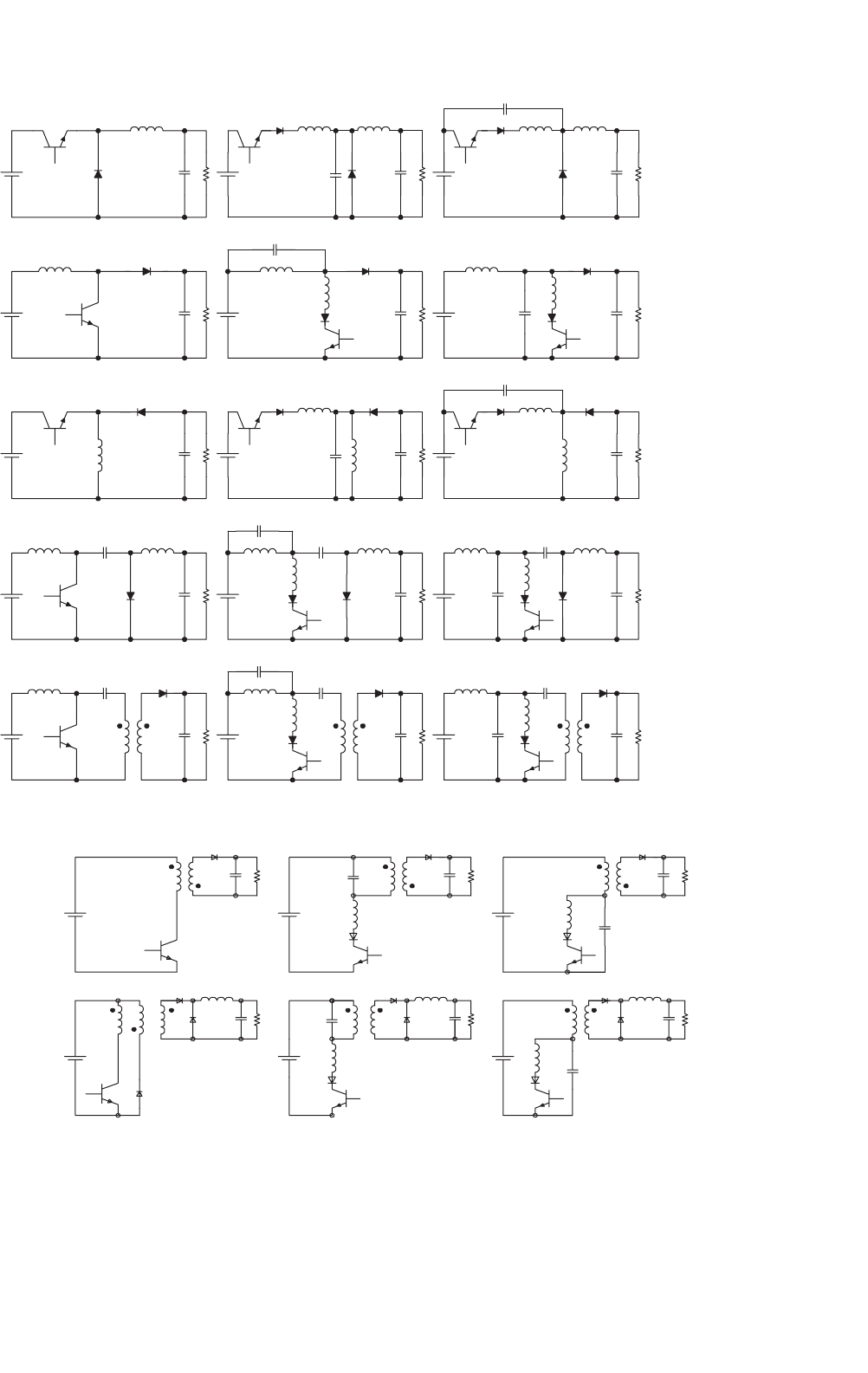
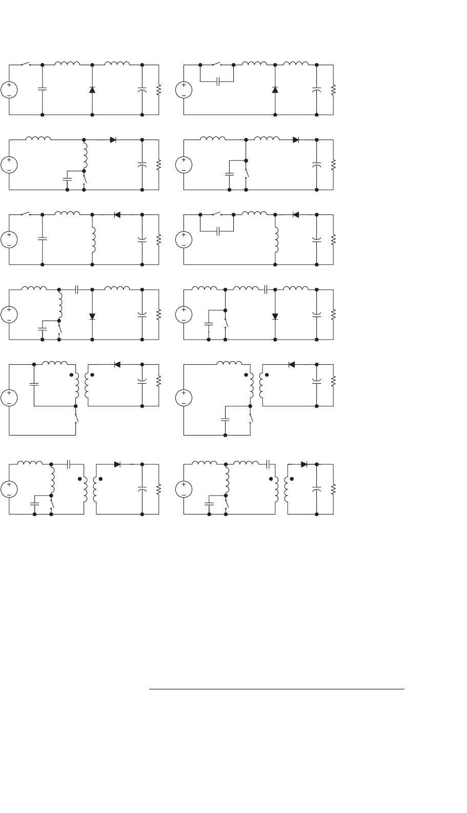
By replacing the switch in the conventional converters,
a family of QRC [9] with ZCS is shown in Fig. 16.7.
16.4.2 ZVS-QRC
In these converters, the resonant capacitor provides a zero-
voltage condition for the switch to turn on and off.
16 Resonant and Soft-switching Converters 411
BUCK
S1
D1 L1
C1
S1
D1 L1
C1
BOOST
C1
L1
D1
BUCK/
BOOST
L1
C1
D1
S1
D1 L1
C1
S1
D1 L1
C1
CUK
C1
L1
D1
L1
C1
D1
SEPIC
C1
L1
D1
L1
C1
D1
FLYBACK
C1
L1
D1
L1
D1
C1
FORWARD L1
D1
C1
C1
L1
D1
FIGURE 16.7 A family of quasi-resonant converter with ZCS.

412 S. Y. Hui and H. S. H. Chung
A quasi-resonant buck converter designed for half-wave oper-
ation is shown in Fig. 16.8a – using a ZV resonant switch
in Fig. 16.4b. The steady-state circuit waveforms are shown
in Fig. 16.8b. Basic relations of ZVS-QRCs are given in
Eqs. (16.1a–e). When the switch S is turned on, it carries the
output current I
o
. The supply voltage V
i
reverse biases the
diode D
f
. When the switch is zero-voltage (ZV) turned off,
the output current starts to flow through the resonant capaci-
tor C
r
. When the resonant capacitor voltage V
Cr
is equal to V
i
,
D
f
turns on. This starts the resonant stage. When V
Cr
equals
zero, the anti-parallel diode turns on. The resonant capacitor
is shorted and the source voltage is applied to the resonant
inductor L
r
. The resonant inductor current I
Lr
increases lin-
early until it reaches I
o
. Then D
f
turns off. In order to achieve
ZVS, S should be triggered during the time when the anti-
parallel diode conducts. It can be seen from the waveforms that
the peak amplitude of the resonant capacitor voltage should
be greater or equal to the input voltage (i.e. I
o
Z
r
> V
in
). From
Fig. 16.8c, it can be seen that the voltage conversion ratio is
load-sensitive. In order to regulate the output voltage for dif-
ferent loads r, the switching frequency should also be changed
accordingly.
ZVS converters can be operated in full-wave mode. The cir-
cuit schematic is shown in Fig. 16.9a. The circuit waveforms in
steady state are shown in Fig. 16.9b. The operation is similar
to half-wave mode of operation, except that V
Cr
can swing
between positive and negative voltages. The relationships
between M and g at different r are shown in Fig. 16.9c.
Comparing Fig. 16.8c with Fig. 16.9c, it can be seen that M is
load-insensitive in full-wave mode. This is a desirable feature.
However, as the series diode limits the direction of the switch
current, energy will be stored in the output capacitance of the
switch and will dissipate in the switch during turn on. Hence,
the full-wave mode has the problem of capacitive turn-on loss,
and is less practical in high frequency operation. In practice,
ZVS-QRCs are usually operated in half-wave mode rather than
full-wave mode.
By replacing the ZV resonant switch in the conventional
converters, various ZVS-QRCs can be derived. They are shown
in Fig. 16.10.
16.4.3 Comparisons between ZCS and ZVS
ZCS can eliminate the switching losses at turn off and reduce
the switching losses at turn on. As a relatively large capac-
itor is connected across the output diode during resonance,
the converter operation becomes insensitive to the diode’s
junction capacitance. When power MOSFETs are zero-current
switched on, the energy stored in the device’s capacitance will
be dissipated. This capacitive turn-on loss is proportional to
the switching frequency. During turn on, considerable rate
of change of voltage can be coupled to the gate drive cir-
cuit through the Miller capacitor, thus increasing switching
loss and noise. Another limitation is that the switches are
under high current stress, resulting in higher conduction loss.
However, it should be noted that ZCS is particularly effective
in reducing switching loss for power devices (such as IGBT)
with large tail current in the turn-off process.
ZVS eliminates the capacitive turn-on loss. It is suitable
for high-frequency operation. For single-ended configuration,
the switches could suffer from excessive voltage stress, which
is proportional to the load. It will be shown in Section 16.5
that the maximum voltage across switches in half-bridge and
full-bridge configurations is clamped to the input voltage.
For both ZCS and ZVS, output regulation of the resonant
converters can be achieved by variable frequency control. ZCS
operates with constant on-time control, while ZVS operates
with constant off-time control. With a wide input and load
range, both techniques have to operate with a wide switch-
ing frequency range, making it not easy to design resonant
converters optimally.
16.5 ZVS in High Frequency
Applications
By the nature of the resonant tank and ZCS, the peak switch
current in resonant converters is much higher than that in the
square-wave counterparts. In addition, a high voltage will be
established across the switch in the off state after the resonant
stage. When the switch is switched on again, the energy stored
in the output capacitor will be discharged through the switch,
causing a significant power loss at high frequencies and high
voltages. This switching loss can be reduced by using ZVS.
ZVS can be viewed as square-wave power utilizing a con-
stant off-time control. Output regulation is achieved by
controlling the on time or switching frequency. During the off
time, the resonant tank circuit traverses the voltage across the
switch from zero to its peak value and then back to zero again.
At that ZV instant, the switch can be reactivated. Apart from
the conventional single-ended converters, some other exam-
ples of converters with ZVS are illustrated in the following
section.
16.5.1 ZVS with Clamped Voltage
The high voltage stress problem in the single-switch config-
uration with ZVS can be avoided in half-bridge (HB) and
full-bridge (FB) configurations [14–17]. The peak switch volt-
age can be clamped to the dc supply rail, and thus reducing
the switch voltage stress. In addition, the series transformer
leakage and circuit inductance can form parts of the resonant
path. Therefore, these parasitic components, which are unde-
sirable in hard-switched converter become useful components
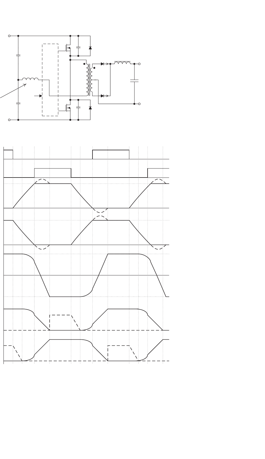
in ZVS ones. Figures 16.11 and 16.12 show the ZVS HB and
FB circuits, respectively, together with the circuit waveforms.
16 Resonant and Soft-switching Converters 413
V
i
C
f
C
r
L
r
L
f
D
f
D
r
+
V
o
−
+
v
oi
−
I
Lr
+ v
c
−
I
o
(a)
t
0
t
1
0 t
t
1
'
t
4
t
3
t
2
'
t
2
t
1
"
I
o
1 cycle
I
L
t
0
t
1
0 t
t
1
'
t
4
t
3
t
2
'
t
2
t
1
"
V
d
v
c
Z
o
I
o
(b)
γ
M
0.5
0.2
0.1
0.8
0.9
(c)
0
0.1
0.2
0.3
0.4
0.5
0.6
0.7
0.8
0.9
1
0 0.1 0.2 0.3 0.4 0.5 0.6 0.7 0.8
0.9
1
FIGURE 16.8 Half-wave, quasi-resonant buck converter with ZVS: (a) schematic diagram; (b) circuit waveforms; and (c) relationship between
M and γ.
414 S. Y. Hui and H. S. H. Chung
C
f
C
r
L
r
L
f
D
f
+
V
o
−
+
v
oi
−
I
Lr
+ v
c
−
D
r
I
o
(a)
0t
t
2
I
o
1 cycle
t
0
t
1
0t
t
1
'
t
4
t
3
t
2
'
t
2
t
1
"
v
c
t
0
t
1
t
1
'
t
4
t
3
t
2
'
t
1
"
I
Lr
v
i
Z
r
I
o
(b)
γ
M
0.9
1
0.2
0.5
0.8
(c)
0
0.1
0.2
0.3
0.4
0.5
0.6
0.7
0.8
0.9
1
0 0.1 0.2 0.3 0.4 0.5 0.6 0.7 0.8
0.9
1
FIGURE 16.9 Full-wave, quasi-resonant buck converter with ZVS: (a) schematic diagram; (b) circuit waveforms; and (c) relationship between
M and γ.
The resonant capacitor is equivalent to the parallel connection
of the two capacitors (C
r
/2) across the switches. The off-state
voltage of the switches will not exceed the input voltage during
resonance because they will be clamped to the supply rail by
the anti-parallel diode of the switches.
16.5.2 Phase-shifted Converter with Zero
Voltage Transition
In a conventional FB converter, the two diagonal switch pairs
are driven alternatively. The output transformer is fed with an
16 Resonant and Soft-switching Converters 415
Buck
Boost
Buck–boost
Cuk
Flyback
Sepic
FIGURE 16.10 A family of quasi-resonant converter with ZVS.
ac rectangular voltage. By applying a phase-shifting approach,
a deliberate delay can be introduced between the gate sig-
nals to the switches [18]. The circuit waveforms are shown in
Fig. 16.13. Two upper or lower switches can be conducting
(either through the switch or the anti-parallel diode), yet the
applied voltage to the transformer is zero. This zero-voltage
condition appears in the interval [t
1
, t
2
]ofV
pri
in Fig. 16.13.
This operating stage corresponds to the required off time for
that particular switching cycle. When the desired switch is
turned off, the primary transformer current flows into the
switch output capacitance causing the switch voltage to res-
onate to the opposite input rail. Effects of the parasitic circuit
components are used advantageously to facilitate the resonant
transitions. This enables a ZVS condition for turning on the
opposite switch. Thus, varying the phase shift controls the
effective duty cycle and hence the output power. The resonant
circuit is necessary to meet the requirement of providing suf-
ficient inductive energy to drive the capacitors to the opposite
bus rail. The resonant transition must be achieved within the
designed transition time.
16.6 Multi-resonant Converters (MRC)
The ZCS- and ZVS-QRCs optimize the switching condition
for either the active switch or the output diode only, but not
416 S. Y. Hui and H. S. H. Chung
t
0
V
IN
V
IN
0
0
0
0
0
V
IN
/2
V
IN
/2
I
o
/N
−I
o
/N
−V
D1
−V
D2
I
out
I
out
t
0
t
0
t
0
t
1
t
1
t
1
t
2
t
2
t
2
t
3
t
3
t
3
t
4
t
4
ON
ON
OFF
OFF
t
4
t
3
t
2
t
1
t
2
t
1
t
0
t
3
C
r
/2
C
r
/2
L
1
L
R
Q
2
Q
1
D
1
D
2
n:1
I
1
T
1
I
2
V
i
V
o
Leakage
inductance
C
o
Control
Circuit
(a)
(b)
FIGURE 16.11 Half-bridge converter with ZVS: (a) circuit diagram and (b) circuit waveforms.
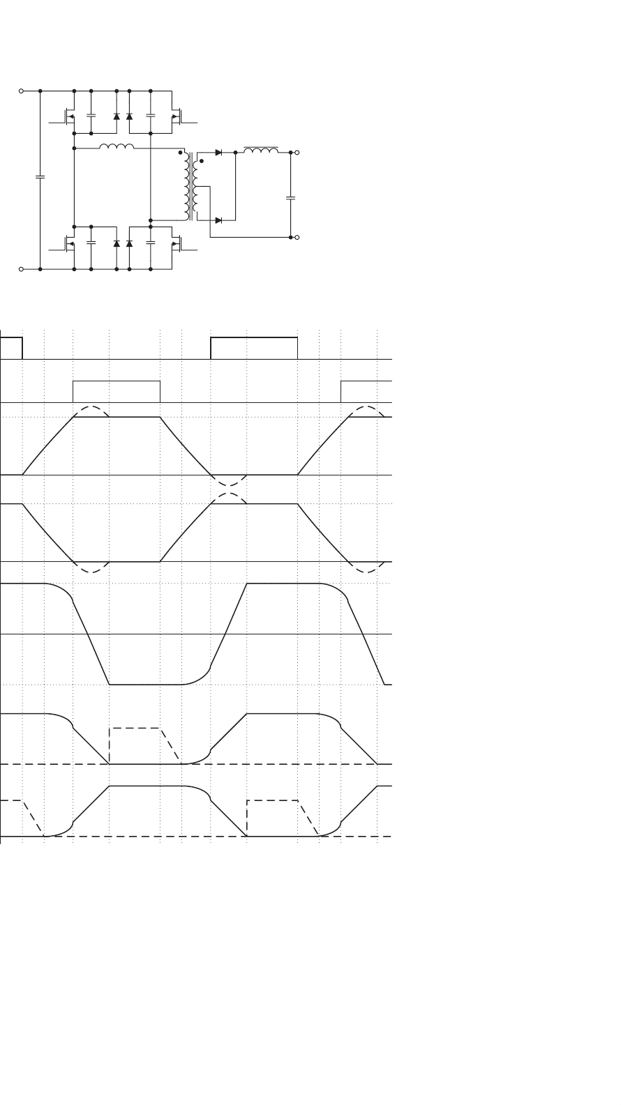
16 Resonant and Soft-switching Converters 417
(a)
C
1
C
x
C
x
C
x
C
x
L
1
Q
1
Q
4
D
1
D
2
T
1
n:1
V
i
V
o
L
R
Q
3
Q
2
C
o
t
0
V
IN
V
IN
0
0
0
0
0
V
IN
/2
V
IN
/2
I
o
/N
−I
o
/N
−V
D1
−V
D2
I
OUT
I
OUT
t
0
t
0
t
0
t
1
t
1
t
1
t
2
t
2
t
2
t
3
t
3
t
3
t
4
t
4
ON
ON
OFF
OFF
t
4
t
3
t
2
t
1
t
2
t
1
t
0
t
3
(b)
FIGURE 16.12 Full-bridge converter with ZVS: (a) circuit schematics and (b) circuit waveforms.