Power electronic handbook
Подождите немного. Документ загружается.

388 J. R. Espinoza
ωt
i
i
Zone I Zone II Zone III
(a)
ωt
v
ab
v
i
(b)
ωt
v
an
0.667 v
i
(c)
ωt
e
a
i
la
(d)
ωt
p
l
180 540 720 900 1080
180 720 1080
180 540 720 900 1080
180 540 900 1080
180 540 720 900 1080
(e)
360
360
360360 540540 900900
360360
360
360 540 900
360
360360
360
360
360360
360
360
720
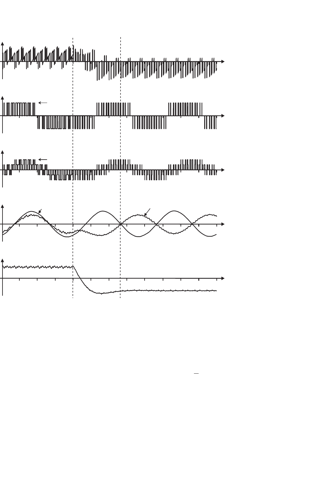
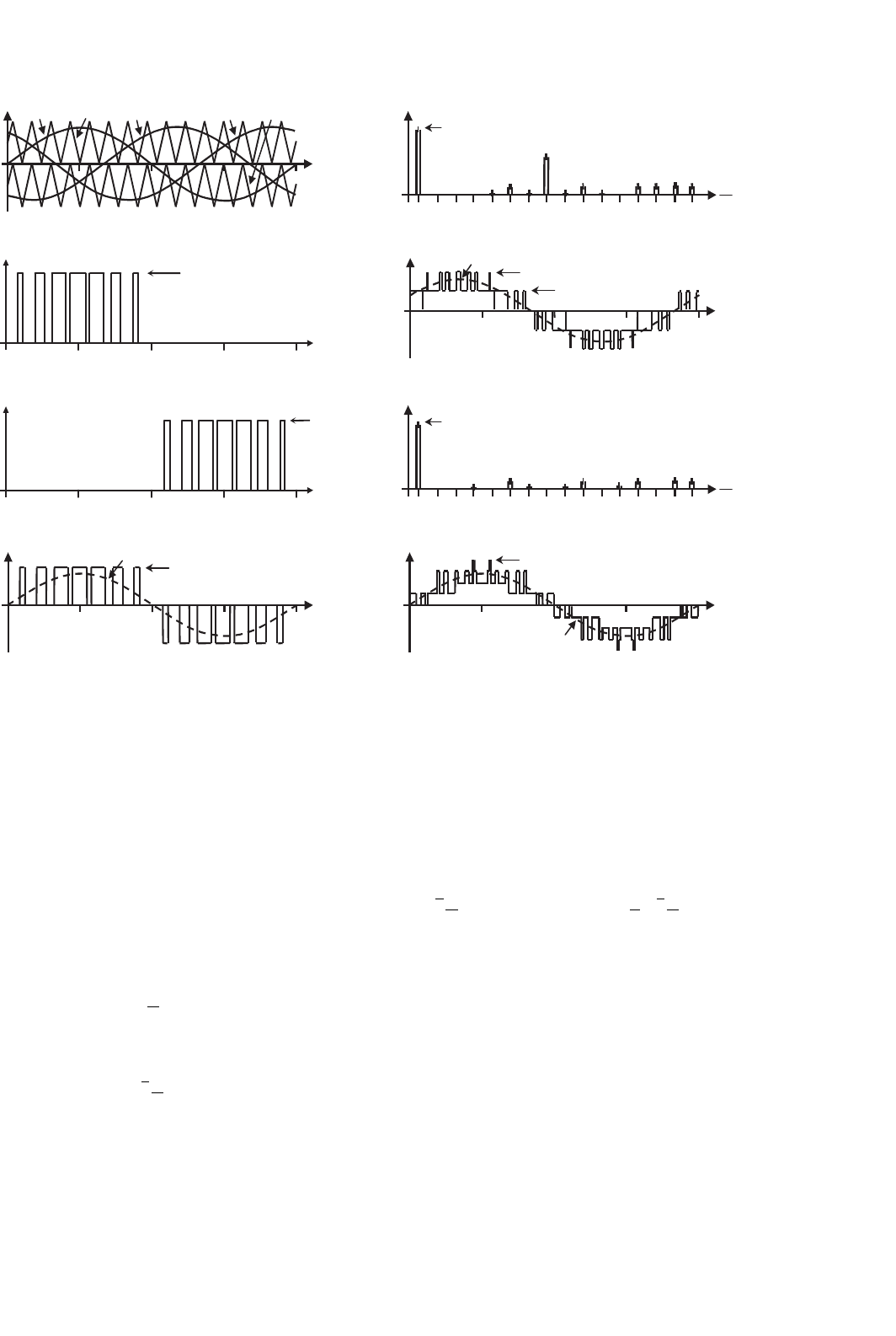
FIGURE 15.49 The ASD based on a VSI. Motoring to regenerative operating mode transition: (a) dc bus current; (b) ac line motor voltage; (c) ac
phase motor voltage; (d) motor line current and back-emf; and (e) shaft power.
Figure 15.49 shows a transition from the motoring to regen-
erative operating mode for an ASD as shown in Fig. 15.47.
Here, a stiff dc bus voltage has been used. Zone I in Fig. 15.49
is the motoring mode, Zone II is a transition condition, and
Zone III is the regeneration mode. The line voltage is adjusted
dynamically to obtain nominal motor line currents during
regeneration (Fig. 15.49d). Zone III clearly shows that the shaft
power gets reversed.
Occasional regeneration means that the drive rarely goes
into this operating mode. Therefore, such energy can be:
(a) left uncontrolled or (b) burned in resistors that are par-
alleled to the dc bus. The first option is used in low- to
medium-power applications that use diode-based front-end
rectifiers. Therefore, the dc bus current flows into the dc bus
capacitor and the dc bus voltage rises accordingly to
v
i
=
1
C
I
i
t (15.87)
where v
i
is the dc bus voltage variation, C is the dc bus
voltage capacitor, I
i
is the average dc bus current during regen-
eration, and t is the duration of the regeneration operating
mode. Usually, the drives have the capacitor C designed to
allow a 10% overvoltage in the dc bus.
The second option uses burning resistors R
R
that are par-
alleled in the dc bus as shown in Fig. 15.50 by means of the
15 Inverters 389
v
as
i
oa
+
−
v
ab
N
i
i
+
−
v
i
/2
+
−
C
+
C
−
i
ob
i
oc
+
−
v
bc
a
b
c
VSI
v
an
v
bn
v
cn
n
Diode
Rectifier
i
sa
v
bs
v
cs
R
L
e
a
e
b
e
c
S
R
R
R
v
i
/2
FIGURE 15.50 The ASD based on a VSI. Burning resistor strategy.
switch S
R
. A closed-loop strategy based on the actual dc bus
voltage modifies the duty cycle of the turn-on/turn-off of the
switch S
R
in order to keep such voltage under a given refer-
ence. This alternative is used when the energy recovered by the
VSI would result in an acceptable dc bus voltage variation if
an uncontrolled alternative is used.
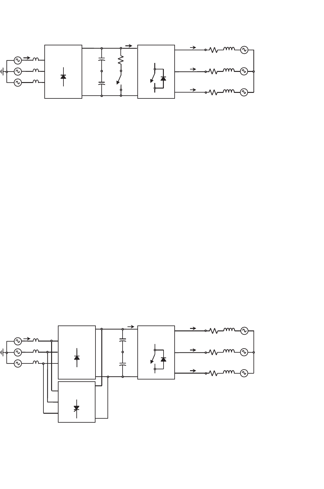
There are some special cases where the regeneration operat-
ing mode is frequently used. For instance, electrical shovels in
mining companies have repetitive working cycles and ≈15%
of the energy is sent back into the dc bus. In this case, a valid
alternative is to send back the energy into the ac distribution
system.
The schematic shown in Fig. 15.51 is capable of taking the
kinetic energy and sending it into the ac grid. As reviewed
earlier, the regeneration operating mode reverses the polarity
of the dc current i
i
, and because the diode-based front-end
converter cannot take negative currents, a thyristor-based
front-end converter is added. Similarly to the burning-resistor
approach, a closed-loop strategy based on the actual dc bus
voltage v
i
modifies the commutation angle α of the thyris-
tor rectifier in order to keep such voltage under a given
reference.
v
as
i
oa
+
−
v
ab
N
i
i
+
−
v
i
/2
+
−
C
+
C
−
i
ob
i
oc
+
−
v
bc
a
b
c
VSI
v
an
v
bn
v
cn
n
Diode
Rectifier
i
sa
v
bs
v
cs
R
L
e
a
e
b
e
c
Thyristor
Rectifier
v
i
/2
FIGURE 15.51 The ASD based on a VSI. Diode-thyristor-based front-end rectifier with regeneration capabilities.
B. Regenerative Operating Mode as Normal operating Mode
Fewer industrial applications are capable of returning energy
into the ac distribution system on a continuous basis. For
instance, mining companies usually transport their product
downhill for a few kilometers before processing it. In such
cases, the drive maintains the transportation belt conveyor at
constant speed and takes the kinetic energy. Due to the large
amount of energy and the continuous operating mode, the
drive should be capable of taking the kinetic energy, trans-
forming it into electrical energy, and sending it into the ac
distribution system. This would make the drive a generator
that would compensate for the active power required by other
loads connected to the electrical grid.
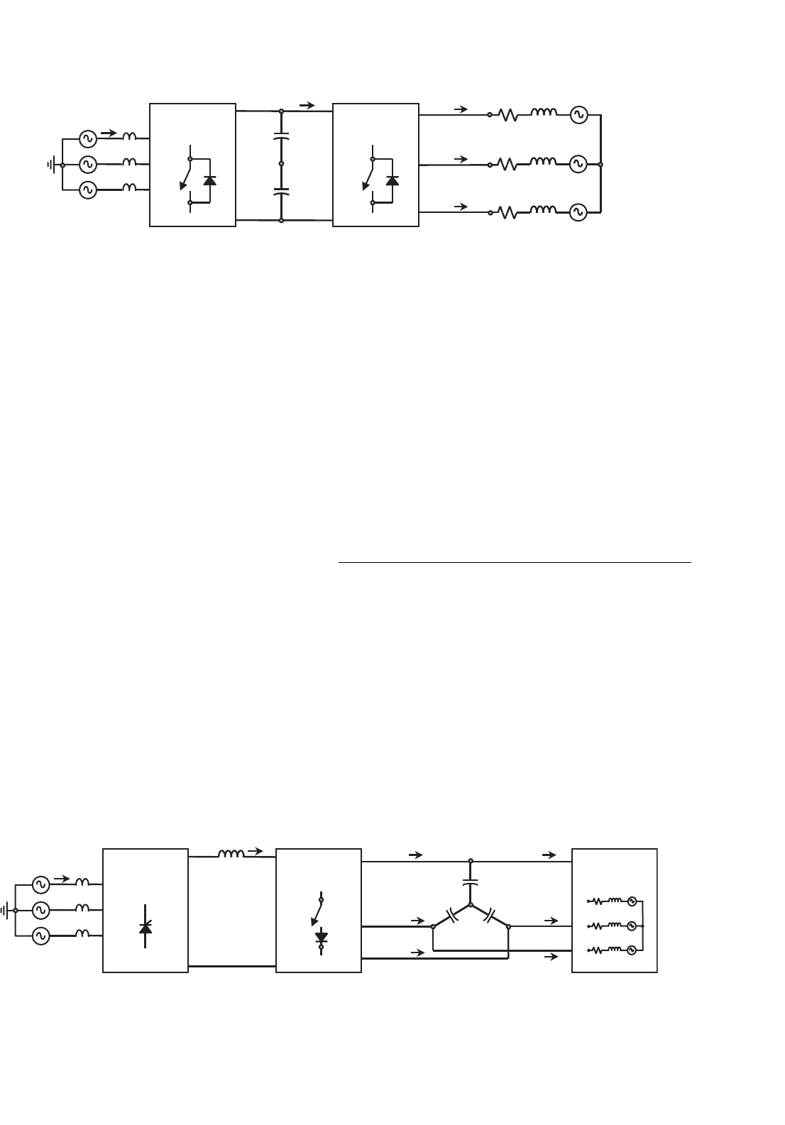
The schematic shown in Fig. 15.52 is a modern alternative
for adding regeneration capabilities to the VSI-based drive on
a continuous basis. In contrast to the previous alternatives, this
scheme uses a VSI topology as an active front-end converter,
which is generally called voltage-source rectifier (VSR). The
VSR operates in two quadrants, that is, positive dc voltages and
positive/negative dc currents as reviewed earlier. This feature
makes it a perfect match for ASDs based on a VSI. Some of
the advantages of using a VSR topology are: (i) the ac supply
390 J. R. Espinoza
v
as
i
oa
+
−
v
ab
N
i
i
+
−
v
i
/2
+
−
C
+
C
−
i
ob
i
oc
+
−
v
bc
a
b
c
VSI
v
an
v
bn
v
cn
n
i
sa
v
bs
v
cs
R
L
e
a
e
b
e
c
VSR
v
i
/2
FIGURE 15.52 The ASD based on a VSI. Active front-end rectifier with regeneration capabilities.
current can be as sinusoidal as required (by increasing the
switching frequency of the VSR or the ac line inductance);
(ii) the operation can be done at a unity displacement power
factor in both motoring and regenerative operating modes;
and (iii) the control of the VSR is done in both motoring and
regenerative operating modes by a single dc bus voltage loop.
15.6.3 Regenerative Operating Mode in
Three-phase CSIs
There are drives where the motor side converter is a CSI. This
is usually the case where near sinusoidal motor voltages are
needed instead of the PWM type of waveform generated by
VSIs. This is normally the case for medium-voltage appli-
cations. Such inverters require a dc current source that is
constructed by means of a controlled rectifier.
Figure 15.53 shows a CSI-based ASD where the dc current
source is generated by means of a thyristor-based rectifier in
combination with a dc link inductor L
dc
. In order to main-
tain a constant dc link current i
i
= I
i
, the thyristor-based
rectifier adjusts the commutation angle α by means of a closed-
loop control strategy. Assuming a constant dc link current,
the regenerating operating mode is achieved when the dc link
voltage v
i
reverses its polarity. This can be done by modify-
ing the PWM pattern applied to the CSI as in the VSI-based
drive. To maintain the dc link current constant, the thyristor-
based rectifier also reverses its dc link voltage v
r
. Fortunately,
the thyristor rectifier operates in two quadrant, that is, pos-
itive dc link currents and positive/ negative dc link voltages.
i
oa
+
−
v
ab
i
ob
i
oc
+
−
v
bc
a
b
c
CSI
i
la
i
lc
i
lb
ac machine
n
R
L
e
a
e
b
e
c
v
as
i
i
i
sa
v
bs
v
cs
+
−
v
i
+
−
v
r
L
dc
v
an
v
bn
v
cn
+
−
+
+
n
C
Thyristor
Rectifier
FIGURE 15.53 The ASD based on a CSI. Thyristor-based rectifier.
Thus, no additional equipment is required to include regener-
ation capabilities in CSI-based drives.
Similarly, an active front-end rectifier could be used
to improve the overall performance of the thyristor-based
rectifier. A PWM current-source rectifier (CSR) could replace
the thyristor-based rectifier with the following added advan-
tages: (i) the ac supply current can be as sinusoidal as required
(e.g. by increasing the switching frequency of the CSR); (ii) the
operation can be done at a unity displacement power factor in
both motoring and regenerative operating modes; and (iii) the
control of the CSR is done in both motoring and regenerative
operating modes by a single dc bus current loop.
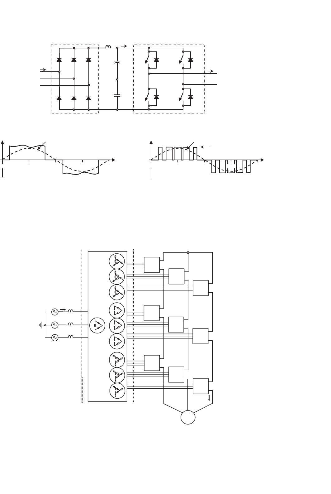
15.7 Multistage Inverters
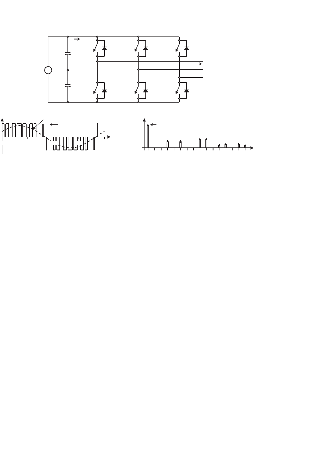
The most popular three-phase voltage source inverter (VSI)
consists of a six-switch topology (Fig. 15.54a). The topol-
ogy can generate a three-phase set of ac line voltages such
that each line voltage v
ab
(Fig. 15.54b) features a fundamen-
tal ac line voltage v
ab1
and unwanted harmonics Fig. 15.54c.
The fundamental ac line voltage is usually required as a sinu-
soidal waveform at variable amplitude and frequency, and the
unwanted harmonics are located at high frequencies. These
requirements are met by means of a modulating technique as
shown earlier. Among the applications in low-voltage ranges
of six-switch VSIs are the adjustable speed drives (ASDs). The
range is in low voltages due to: (a) the high dv/dt present in the
PWM ac line voltages (Fig. 15.54b), which will be unacceptable
15 Inverters 391
+
−
v
i
S
1
a
S
4
D
1
D
4
S
3
b
S
6
D
3
D
6
i
oa
+
−
v
ab
S
5
c
S
2
D
5
D
2
N
i
i
+
−
v
i
/2
v
i
/2
+
−
C
+
C
−
(a)
90 360
ωt
v
ab
v
ab1
v
i
157931923312711511317212925
v
ab
f
f
o
0.8·0.866·v
i
(b)
(c)
2700 180
FIGURE 15.54 Six-switch voltage source inverter (m
f
= 9, m
a
= 0.8): (a) power topology; (b) ac output voltage; and (c) ac output voltage spectrum.
in the medium- to high-voltage ranges and (b) the load power
would be shared only among six switches. This may require
paralleling and series-connected power valves, an option usu-
ally avoided as symmetrical sharing of the power is not natural
in these arrangements.
Two solutions are available to generate near-sinusoidal volt-
age waveforms while using six-switch topologies. The first is a
topology based on a CSI in combination with a capacitive filter.
The second solution is a topology based on a VSI including an
inductive or inductive/capacitive filter at the load terminals.
Although both alternatives generate near-sinusoidal voltage
waveforms, both continue sharing the load power only among
six power valves.
Solutions based on multistage voltage source topologies
have been proposed. They provide medium voltages at the
ac terminals while keeping low dv/dts and a large number
of power valves that symmetrically share the total load
power. The multistage VSIs can be classified in multicell and
multilevel topologies.
15.7.1 Multicell Topologies
The goal is to develop a new structure with improved perfor-
mance based on standard structures that are known as cells.
For instance, Fig. 15.55a shows a cell featuring a three-phase
input and a single-phase output. The front-end converter is
a six-diode-based rectifier, and a single-phase VSI generates a
single-phase ac voltage v
o
. Figure 15.55b and c shows charac-
teristic waveforms where a sinusoidal unipolar PWM (m
f
= 6,
m
a
= 0.8) has been used to modulate the inverter.
Standard cells are meant to be used at low voltages, thus
they can use standard components that are less expensive
and widely available. The new structure should generate
near-sinusoidal ac load voltages, draw near-sinusoidal ac line
currents, and more importantly the load voltages should
feature moderate dv/dt s.
Figure 15.56 shows a multicell converter that generates a
three-phase output voltage out of a three-phase ac distribution
system. The structure uses three standard cells (as shown in
Fig. 15.55) connected in series to form one phase; thus the
phase-load voltages are the sum of the single-phase voltages
generated by each cell. For instance, the phase voltage a is
given by
v
an
= v
o11
+v
o21
+v
o31
(15.88)
In order to maximize the load-phase voltages, the ac voltages
generated by the cells should feature identical fundamental
components. On the other hand, each cell generates a PWM
voltage waveform at the ac side, which contains unwanted
voltage harmonics. If a carrier-based modulating technique is
used, the harmonics generated by each cell are at well-defined
frequencies (Fig. 15.55c). Some of these harmonics are not
present in the phase-load voltage if the carrier signals of each
cell are properly phase shifted.
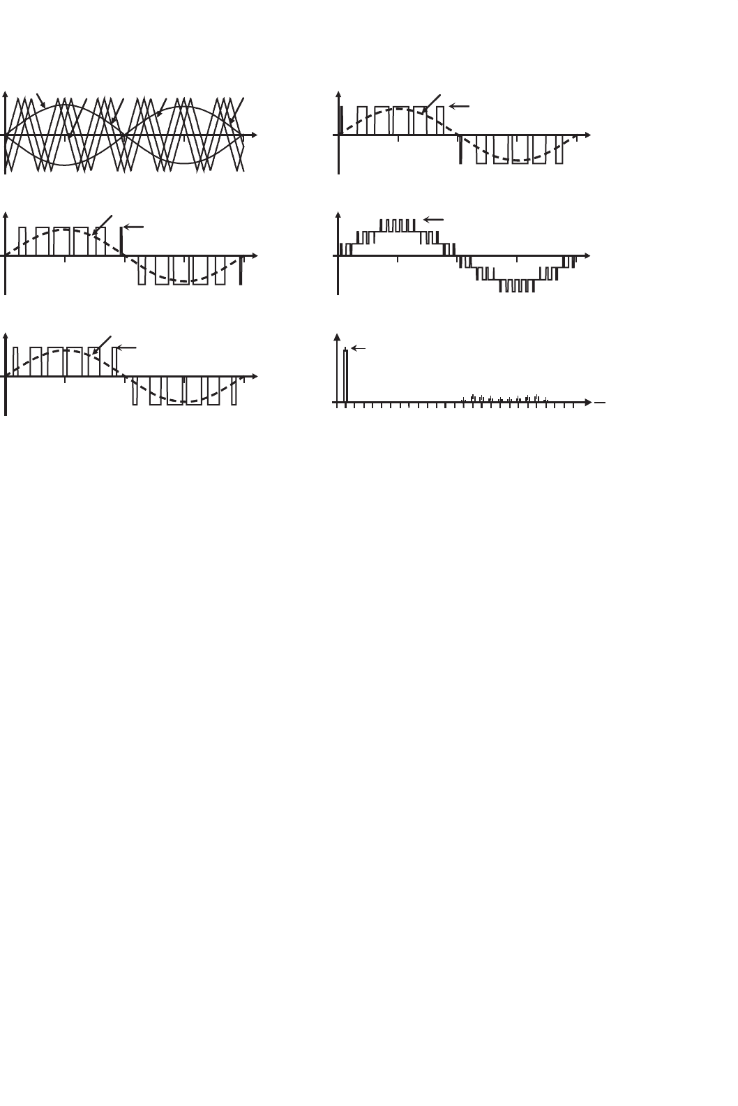
In fact, Fig. 15.57 shows the voltages generated by cells c
11
,
c
21
, and c
31
, which are v
o11
, v
o21
, and v
o31
, respectively, and
form the load-phase voltage a. They are generated using the
unipolar SPWM approach, that is, one modulating signal v
ca
and three carrier signals v
1
, v
2
, and v
3
that are used by
cells c
11
,c
21
, and c
31
, respectively (Fig. 15.57a). The carrier
signals have a normalized frequency m
f
, which ensures an
m
f
switching frequency in each power valve and the lowest
unwanted set of harmonics ≈2·m
f
(m
f
even) in the ac cell
392 J. R. Espinoza
Diode rectifier
i
sa
S
1+
a
S
1−
D
1+
D
1−
i
o
+
−
v
o
S
2+
b
S
2−
D
2+
D
2−
N
i
i
+
−
+
−
C
+
C
−
D
1
D
3
D
5
D
4
D
6
D
2
Single-phase VSI
L
(a)
180 27090 360
ωt
i
sa
i
sa1
18090 360
ωt
v
o
v
o1
v
i
(b) (c)
v
i
/2
0 0 270
FIGURE 15.55 Three-phase-input single-phase output cell: (a) power topology; (b) ac input current, phase a; and (c) ac output voltage (m
f
= 6,
m
a
= 0.8).
multicell
arrangement
ac
mains
IM
C
13
v
as
i
sa
v
a
i
sa
n
C
12
C
11
C
23
C
22
C
21
C
33
C
32
C
31
+
−
v
o11
+
−
+
−
multipulse
transformer
v
o21
v
o31
FIGURE 15.56 Multistage converter based on a multicell arrangement.
15 Inverters 393
wt
v
ca
−v
ca
∆v
1
∆v
2
∆v
3
wt
v
o31
v
o311
v
i
(a) (d)
wt
v
o21
v
o211
v
i
wt
v
an
3·v
i
(b) (e)
wt
180 27090 3600
180 27090 3600
180 27090 3600
180 27090 3600
180 27090 3600
v
o11
v
o111
v
i
25529374917911321334541
v
an
f
f
o
3·0.8·v
i
(c) (f)
FIGURE 15.57 Multicell topology. Cell voltages in phase a using a unipolar SPWM (m
f
= 6, m
a
= 0.8): (a) modulating and carrier signals; (b) cell
c
11
ac output voltage; (c) cell c
21
ac output voltage; (d) cell c
31
ac output voltage; (e) phase a load voltage; and (f) phase a load-voltage spectrum.
voltages v
o11
, v
o21
, and v
o31
. More importantly, the carrier
signals are ψ = 60
◦
out-of-phase, which ensures the lowest
unwanted set of voltage harmonics ≈6 ·m
f
in the load-phase
voltage v
an
, that is, the lowest set of harmonics in Fig. 15.57f
is 6 · m
f
= 6 ·6 = 36.
This can be explained as follows. The voltage harmonics
present in the PWM voltage of each cell are at l · m
f
± k,
l = 2, 4, ... (where k = 1, 3, 5, ...); for instance, for m
f
= 6,
the first set of harmonics is at 12 ± 1, 12 ± 3, … in all cells.
Because the cells in one phase use carrier signals that are 60
◦
out-of-phase, all the voltage harmonics ≈l ·m
f
in all cells are
l ·60
◦
out-of-phase. Therefore, for l = 2, the cell c
11
generates
the harmonics l · m
f
± k = 2 · m
f
± k at a given phase ϕ,
the cell c
21
generates the harmonics 2 · m
f
± k at a phase
ϕ + l · 60
◦
= ϕ + 2 · 60
◦
= ϕ + 120
◦
= ϕ − 240
◦
, and
the cell c
21
generates the harmonics 2 · m
f
± k at a phase
ϕ − l · 60
◦
= ϕ − 2 · 60
◦
= ϕ − 120
◦
= ϕ + 240
◦
; thus, if
the voltages have identical amplitudes, the harmonics ≈2 ·m
f
add up to zero. Similarly, for l = 4, the cell c
11
generates
the harmonics l · m
f
± k = 4 · m
f
± k at a given phase ϕ,
the cell c
21
generates the harmonics 4 · m
f
± k at a phase
ϕ + l · 60
◦
= ϕ + 4 · 60
◦
= ϕ + 240
◦
= ϕ − 120
◦
, and
the cell c
21
generates the harmonics 4 · m
f
± k at a phase
ϕ − l · 60
◦
= ϕ − 4 · 60
◦
= ϕ − 240
◦
= ϕ + 120
◦
; thus, if
the voltages have identical amplitudes, the harmonics ≈4 ·m
f
add up to zero. However, for l = 6, the cell c
11
generates
the harmonics l · m
f
± k = 6 · m
f
± k at a given phase ϕ,
the cell c
21
generates the harmonics 6 · m
f
± k at a phase
ϕ + l · 60
◦
= ϕ + 6 · 60
◦
= ϕ + 360
◦
= ϕ, and the cell c
21
generates the harmonics 6 · m
f
± k at a phase ϕ − l · 60
◦
=
ϕ −6 ·60
◦
= ϕ −360
◦
= ϕ; thus, if the voltages have identical
amplitudes, the harmonics ≈6 ·m
f
become triplicated rather
than cancelled out.
In general, due to the fact that n
c
= 3, cells are connected in
series in each phase, n
c
carriers are required, which should be
ψ = 180
◦
/n
c
out-of-phase. The number of cells per phase
n
c
depends on the required phase voltage. For instance, a
600 V dc cell generates an ac voltage of ≈600/
√
2 = 424 V.
Then three cells connected in series generate a phase voltage of
3· 424 = 1.27 kV, which in turn generates a 1.27·
√
3 = 2.2 kV
line-to-line voltage.
Phases b and c are generated similarly to phase a. However,
the modulating signals v
cb
and v
cc
should be 120
◦
out-of-
phase. In order to use identical carrier signals in phases b
and c, the carrier-normalized frequency m
f
should be a multi-
ple of 3. Thus, three modulating signals and n
c
carrier signals
are required to generate three phase voltages by means of a
multicell approach, where n
c
depends upon the required load
line voltage and the dc bus voltage of each cell.
The ac supply current of each cell is a six-pulse type of cur-
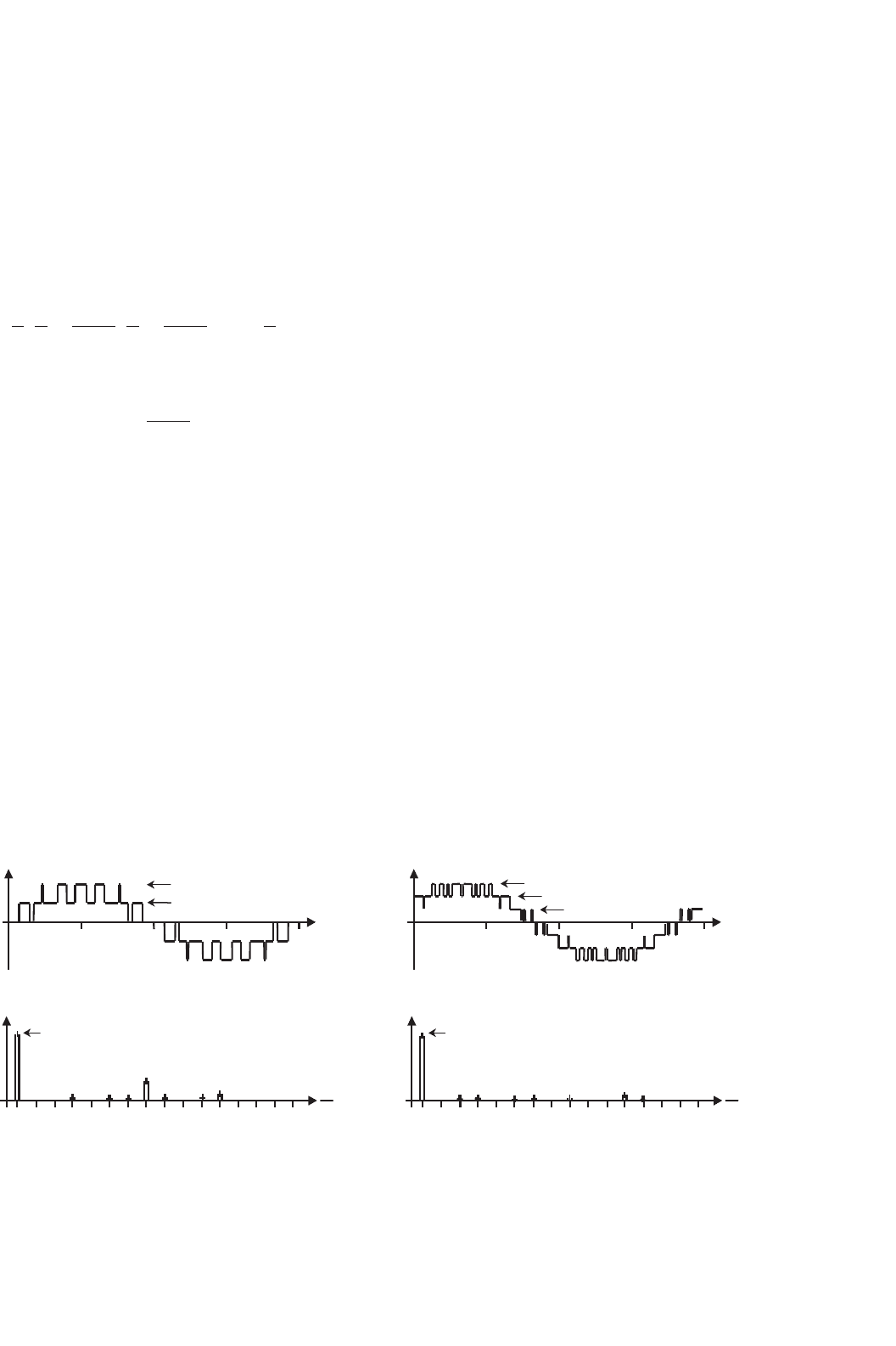
rent as shown in Fig. 15.58, which feature harmonics at 6·k ±1
(k = 1, 2, ...). Similarly to the load side, the ac supply currents
of each cell are combined so as to achieve high-performance
overall supply currents. Because the front-end converter of
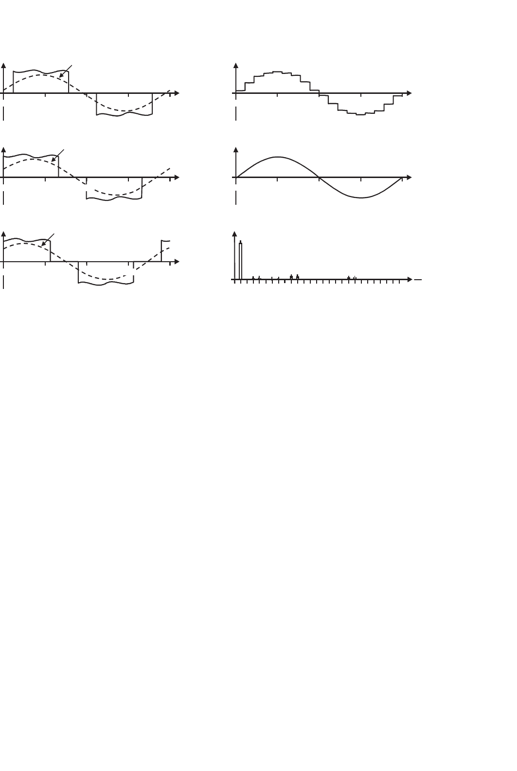
394 J. R. Espinoza
180 270
ωt
i
a11
i
a111
180 27090 360
ωt
i
sa
(a) (d)
270
ωt
i
a21
i
a211
180 27090 360
ωt
v
sa
(b) (e)
90 360
ωt
i
a31
i
a311
25529374991131721334541
i
sa
f
f
o
(c)
(f)
90 36000
18090 36000
180 2700
FIGURE 15.58 Multicell topology. Ac input current, phase a: (a) cell c
11
; (b) cell c
21
; (c) cell c
31
; (d) overall supply current; (e) supply phase voltage;
and (f) overall supply current spectrum.
each cell is a six-pulse diode rectifier, a multipulse approach
is used. This is based on the natural harmonic cancellation
when, for instance, a wye to delta/wye transformer is used
to form an N = 12-pulse configuration from two six-pulse
diode rectifiers. In this case, the fifth and seventh harmon-
ics are cancelled out because the supply voltages applied to
each six-pulse rectifier become 30
◦
out-of-phase. In general,
to form an N = 6 · n
s
pulse configuration, n
s
set of supply
voltages that should be 60
◦
/n
s
out-of-phase is required. This
would ensure the first set of unwanted current harmonics at
6 ·n
s
±1.
The configuration depicted in Fig. 15.56 contains n
c
= 9
cells, and a transformer capable of providing n
s
= 9 sets of
three-phase voltages that should be 60
◦
/n
s
= 60
◦
/9 out-of-
phase to form an N = 6 · n
s
= 6 ·9 = 54-pulse configuration
is required. Although this alternative would provide a near-
sinusoidal overall supply current, a fewer number of pulses are
also acceptable that would reduce the transformer complexity.
An N = 18-pulse configuration usually satisfies all the require-
ments. In the example, this configuration can be achieved by
means of a transformer with n
c
= 9 isolated secondaries;
however, only n
s
= 3 set of three-phase voltages that are
60
◦
/n
s
= 60
◦
/3 = 20
◦
out-of-phase are generated (Fig. 15.56).
The configuration of the transformer restricts the connection
of the cells in groups of three as shown in Fig. 15.56. In this
case, the fifth, seventh, eleventh, and thirteenth harmonics are
cancelled out and thus the first set of harmonics in the supply
currents are the seventeenth and the nineteenth. Figure 15.58d
shows the resulting supply current that is near-sinusoidal and
Fig. 15.58f shows the corresponding spectrum. The fifth, sev-
enth, eleventh, and thirteenth harmonics are still there, which
is due to the fact that the ac input currents in each cell are not
exactly the six-pulse type of waveforms as seen in Fig. 15.58a,
b, and c. This is mainly because: (i) the dc link in the cells
contains a small inductor L, which does not smooth out suffi-
ciently the dc bus current (Fig. 15.55a) and (ii) the transformer
leakage inductance (or added line inductance) smoothes out
the edges of the current, which also contributes to the reactive
power required by the cells. This last effect is not shown in
Fig. 15.58a, b, and c.
15.7.2 Voltage Source-based Multilevel
Topologies
The six-switch VSI is usually called a two-level VSI due to
the fact that the inverter phase voltages v
aN
, v
bN
, and v
cN
(Fig. 15.54a) are instantaneously either v
i
/2 or −v
i
/2. In other
words, the phase voltages can take one of the two voltage levels.
Multilevel topologies provide an alternative to these voltages to
take one value out of N levels. For instance, Fig. 15.59 shows an
N = 3-level topology, where the values of the inverter phase
voltage are either v
i
/2, 0, or −v
i
/2 (Fig. 15.60d). An inter-
esting problem is how to obtain the gating pattern for the
12 switches required in an N = 3-level topology. There
are several modulating techniques to overcome this problem,
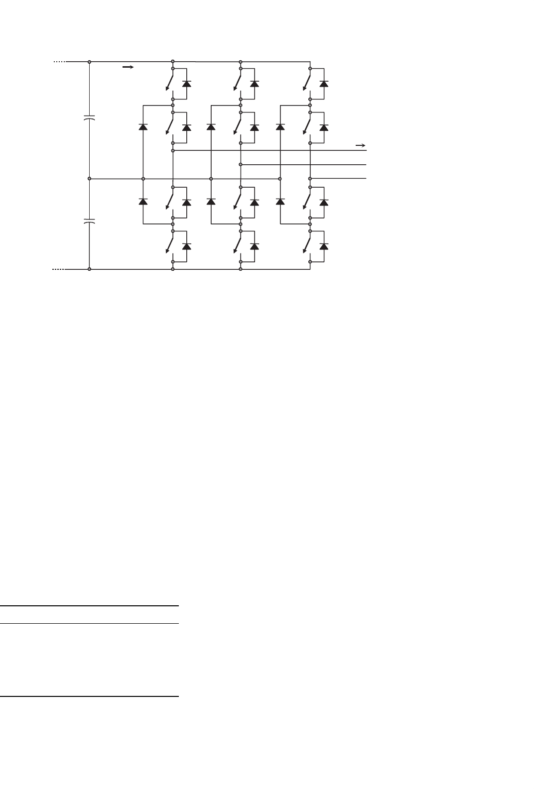
15 Inverters 395
N
i
i
+
−
v
i
/2
+
−
C
+
C
−
a
b
i
oa
+
−
v
ab
c
S
1a
S
1b
D
1a
D
1b
S
3a
S
3b
D
3a
D
3b
S
5a
S
5b
D
5a
D
5b
S
4a
S
4b
D
4a
D
4b
S
6a
S
6b
D
6a
D
6b
S
2a
S
2b
D
2a
D
2b
D
a+
D
a−
D
b+
D
b−
D
c+
D
c−
v
i
/2
FIGURE 15.59 Three-phase three-level VSI topology.
which can be classified as analog (e.g. carrier-based) and dig-
ital (SV-based). Both approaches have to deal with the valid
switch states of the inverter.
A. Valid Switch States in a Three-level VSI
The easiest way of obtaining the valid switch states is to
analyze each phase separately. Phase a contains the switches
S
1a
, S
1b
, S
4a
, and S
4b
, which cannot be on simultaneously
because a short circuit across the dc bus would be produced,
and cannot be off simultaneously because an undefined phase
voltage v
aN
would be produced. A summary of the valid switch
combinations is given in Table 15.7. It is important to note
that all valid switch combinations satisfy the condition that
switch S
1a
state is always the opposite to switch S
4a
state,
and that switch S
1b
state is always the opposite to switch
S
4b
state. Any other switch-state combination would result in
an undefined inverter phase a voltage because it will depend
upon the load-phase current i
oa
polarity. The switch states
for phases b and c are identical to that of phase a; moreover,
TABLE 15.7 Valid switch states for a three-level
VSI, phase a
s
1a
s
1b
s
4a
s
4b
v
o
Components conducting
1100v
i
/2 S
1a
, S
1b
if i
oa
> 0
D
1a
, D
1b
if i
oa
< 0
01100 S
1b
, D
a+
if i
oa
> 0
S
4a
, D
a−
if i
oa
< 0
0011−v
i
/2 D
4a
, D
4b
if i
oa
> 0
S
4a
, S
4b
if i
oa
< 0
because they are paralleled, they can operate in an independent
manner.
B. The SPWM Technique in Three-level VSIs
The main objective is to generate the appropriate 12 gating sig-
nals so as to obtain fundamental inverter phase voltages equal
to a given set of modulating signals. Specifically, the SPWM
in three-level inverters uses a sinusoidal set of modulating sig-
nals (v
ca
, v
cb
, and v
cc
for phases a, b, and c, respectively) and
N − 1 = 2 triangular type of carrier signals (v
1
and v
2
)as
illustrated in Fig. 15.60a. The best results are obtained if the
carrier signals are in-phase and feature an odd normalized fre-
quency (e.g. m
f
= 15). According to Fig. 15.60a, switch S
1a
is
either turned on if v
ca
> v
1
or off if v
ca
< v
1
, and switch S
1b
is either turned on if v
ca
> v
2
or off if v
ca
< v
2
. Addition-
ally, the switch S
4a
status is obtained as the opposite to switch
S
1a
, and the switch S
4b
status is obtained as the opposite to
switch S
1b
. In order to use the same set of carrier signals to
generate the gating signals for phases b and c, the normalized
frequency of the carrier signal m
f
should be a multiple of 3.
Thus, the possible values are m
f
= 3, 9, 15, 21, ....
Figure 15.60 shows the relevant waveforms for a three-level
inverter modulated by means of a SPWM technique (m
f
= 15,
m
a
= 0.8). Specifically, Fig. 15.60d shows the inverter phase
voltage, which is clearly a three-level type of voltage, and
Fig. 15.60f shows the load line voltage, which shows that the
step voltages are at most v
i
/2. More importantly, the inverter
phase voltage (Fig. 15.60e) contains harmonics at l · m
f
± k
with l = 1, 3, ... and k = 0, 2, 4, ... and at l · m
f
± k with
l = 2, 4, ... and k = 1, 3, ... For instance, the first set of
harmonics (l = 1, m
f
= 15) are at 15, 15 ± 2, 15 ± 4, ...
396 J. R. Espinoza
v
ca
ωt
v
D1
v
D2
v
cc
v
cb
157931923312711511317212925
v
aN
f
f
o
0.8·v
i
/2
(a) (e)
ωt
S
1a
on
180 270 90 360 0
ωt
v
ab
v
ab1
v
i
v
i
/2
b)
(f)
ωt
S
4b
on
180 270 90 360 0
157931923312711511317212925
v
ab
f
f
o
0.8·0.866· v
i
(c) (g)
ωt
v
aN
v
aN1
v
i
/2
ωt
v
an
v
an1
0.66·v
i
(d) (h)
180
180 2702709090 3603600
180
180 2702709090 3603600
180
180 2702709090 3603600 180180 2702709090 3603600
180 27090 3600
180 27090 3600
180 27090 3600 180 27090 3600
FIGURE 15.60 Three-level VSI topology. Relevant waveforms using a SPWM (m
f
= 15, m
a
= 0.8): (a) modulating and carrier signals; (b) switch
S
1a
status; (c) switch S
4b
status; (d) inverter phase a voltage; (e) inverter phase a voltage spectrum; (f) load line voltage; (g) load line voltage spectrum;
and (h) load phase a voltage.
The inverter line voltage (Fig. 15.60g) contains harmonics at
l · m
f
± k with l = 1, 3, ...and k = 2, 4, ... and at l · m
f
± k
with l = 2, 4, ...and k = 1, 3, ...For instance, the first set of
harmonics in the line voltages (l = 1, m
f
= 15) are at 15 ± 2,
15 ±4, ....
All the other features of carrier-based PWM techniques also
apply in multilevel inverters. For instance, (I) the fundamental
component of the inverter phase voltages satisfies
ˆv
aN 1
=ˆv
bN 1
=ˆv
cN 1
= m
a
v
i
2
0 < m
a
≤ 1 (15.89)
and thus the line voltages satisfy
ˆv
ab1
=ˆv
bc1
=ˆv
ca1
= m
a
√
3
v
i
2
0 < m
a
≤ 1 (15.90)
where 0 < m
a
≤ 1 the linear operating region. To further
increase the amplitude of the load voltages, the overmod-
ulation operating region can be used by further increasing
the modulating signal amplitudes (m
a
> 1), where the line
voltages range in
√
3
v
i
2
< ˆv
ab1
=ˆv
bc1
=ˆv
ca1
<
4
π
√
3
v
i
2
(15.91)
Also, (II) the modulating signals could be improved by
adding a third harmonic (zero sequence), which will increase
the linear region up to m
a
= 1.15. This results in a maximum
fundamental line-voltage component equal to v
i
; (III) a non-
sinusoidal set of modulating signals could also be used by the
modulating technique. This is the case where nonsinusoidal
line voltages are required as in active filter applications; and
(IV) because of the two quadrants operation of VSIs, the mul-
tilevel inverter could equally be used in applications where the
active power flow goes from the dc to the ac side or from the
ac to the dc side.
15 Inverters 397
In general, for an N -level inverter modulated by means of
a carrier-based technique, the following conclusions can be
drawn:
(a) three modulating signals 120
◦
out of phase and N −1
carrier signals are required;
(b) the phase voltages in the inverters have a peak value
of v
i
/(N −1);
(c) the phase voltages in the inverters are discrete wave-
forms constructed from the values
v
i
2
,
v
i
2
−
v
i
N −1
,
v
i
2
−
2 ·v
i
N −1
, ···, −
v
i
2
(15.92)
(d) the maximum voltage step in the line voltages is
v
i
N −1
(15.93)
for instance, an N = 5-level inverter requires four
carrier signals, the discrete values of the phase voltages
are: v
i
/2, v
i
/4, 0, −v
i
/4, and −v
i
/2, and the maximum
step voltage at the load side is v
i
/4. Key waveforms are
shown in Fig. 15.61.
One of the drawbacks of the multilevel inverter is that the
dc link capacitors should be equal. Unfortunately, this is not
a natural operating condition mainly due to the fact that the
currents required by the inverter in the dc bus are not sym-
metrical and therefore the capacitors will not equally share
the total dc supply voltage v
i
. To overcome this problem, two
alternatives are developed later on.
C. The Space-vector Modulation in Three-level VSIs
Digital techniques are naturally extended to multilevel
inverters. In fact, the SV modulating technique can be applied
using the same principles used in two-level inverters. However,
ωt
v
aN
v
i
/2
v
i
/4
ωt
v
ab
v
i
2·v
i
/3
v
i
/3
(a) (c)
157931923312711511317212925
v
aN
f
f
o
0.8·v
i
/2
157931923312711511317212925
v
ab
f
f
o
(b) (d)
0.8·0.866· v
i
180180 2702709090 3603600 180180 2702709090 3603600180 27090 3600 180 27090 3600
FIGURE 15.61 Five-level VSI topology. Relevant waveforms using a SPWM (m
f
= 15, m
a
= 0.8): (a) inverter phase a voltage; (b) inverter phase a
voltage spectrum; (c) load line voltage; and (d) load line voltage spectrum.
the higher number of voltage levels increases the complexity
of the practical implementation of the technique. For instance,
in N = 3-level inverters, each leg allows N = 3 different
switch combinations as indicated in Table 15.7. Therefore,
there are N
3
= 27 total valid switch combinations, which
generate N
3
= 27 load line voltages that are represented by
N
3
= 27 space vectors (v
1
, v
2
, ..., v
27
) in Fig. 15.62. For
instance, v
2
= 0.5+j0.866 is due to the line voltages v
ab
= 0.5,
v
bc
= 0.5, v
ca
=−1.0 in pu. Thus, although the principle of
operation is the same, the SV digital algorithm will have to
deal with a higher number of states N
3
. Moreover, because
some space vectors (e.g. v
13
and v
14
in Fig. 15.62) produce the
same load-voltage terminals, the algorithm will have to decide
between the two based on additional criteria and that of the
basic SV-approach. Clearly, as the number of level increases,
the algorithm becomes more and more elaborate. However,
the benefits are not evident as the number of level increases.
The maximum number of levels used in practical applications
is five. This is based on a compromise between the complex-
ity of the implementation and the benefits of the resulting
waveforms.
D. DC Link Voltage Balancing Issues
Figure 15.59 shows a three-level inverter and the ideal wave-
forms are shown in Fig. 15.60, which assume an even distri-
bution of the voltage across the dc link capacitors. This even
distribution is not naturally achieved and could be overcome
by supplying both capacitors from independent supplies or
properly gating the power valves of the inverter in order to
minimize the unbalance.
Figure 15.63 shows an ASD based on a three-level VSI,
where the dc link capacitors are feed from two different
sources. This approach is being commercially used as it
ensures a robust balanced dc link voltage distribution and
operates with a high-performance type of ac mains current.