Power electronic handbook
Подождите немного. Документ загружается.

368 J. R. Espinoza
ωt
v
aN
v
aN1
v
i
/ 2
α
1
α
3
α
2
90 360
ωt
v
ab
v
ab1
v
i
(a) (c)
15793 19 23 312711511317212925
v
aN
f
f
o
0.8
v
i
√3
15793 19 23 312711511317212925
v
ab
f
f
o
0.8·v
i
(b)
(d)
180
180 27027090900 180180 270270180 270900 180 270360360 0360 0
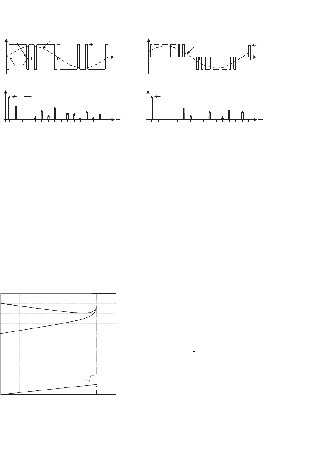
FIGURE 15.18 The three-phase VSI. Ideal waveforms for the SHE technique: (a) phase voltage v
aN
for fifth and seventh harmonic elimination;
(b) spectrum of (a); (c) line voltage v
ab
for fifth and seventh harmonic elimination; and (d) spectrum of (c).
to be solved are:
cos(1α
1
) −cos(1α
2
) +cos(1α
3
) = (2 + π ˆv
aN 1
/v
i
)/4
cos(5α
1
) −cos(5α
2
) +cos(5α
3
) = 1/2
cos(7α
1
) −cos(7α
2
) +cos(7α
3
) = 1/2
(15.35)
where the angles α
1
, α
2
, and α
3
are defined as shown in
Fig. 15.18a and plotted in Fig. 15.19. Figure 15.18b shows
that the third, ninth, fifteenth, ...harmonics are all present in
the phase voltages; however, they are not in the line voltages
(Fig. 15.18d).
0 0.2 0.4 0.6 0.8 1.0
0°
10°
20°
30°
40°
50°
60°
70°
80°
90°
100°
α
1
α
3
α
2
3v
aN1
/v
i
ˆ
FIGURE 15.19 Chopping angles for SHE and fundamental voltage
control in three-phase VSIs: fifth and seventh harmonic elimination.
15.3.5 Space-vector (SV)-based Modulating
Techniques
At present, the control strategies are implemented in digital
systems, and therefore digital modulating techniques are also
available. The SV-based modulating technique is a digital tech-
nique in which the objective is to generate PWM load line
voltages that are on average equal to given load line voltages.
This is done in each sampling period by properly selecting the
switch states from the valid ones of the VSI (Table 15.3) and
by proper calculation of the period of times they are used.
The selection and calculation times are based upon the SV
transformation.
A. Space-vector Transformation
Any three-phase set of variables that add up to zero in the
stationary abc frame can be represented in a complex plane
by a complex vector that contains a real (α) and an imagi-
nary (β) component. For instance, the vector of three-phase
line-modulating signals v
abc
c
=[v
ca
v
cb
v
cc
]
T
can be represented
by the complex vector v
c
= v
ab
c
=[v
cα
v
cβ
]
T
by means of the
following transformation:
v
cα
=
2
3
[
v
ca
−0.5
(
v
cb
+v
cc
)
]
(15.36)
v
cβ
=
√
3
3
(
v
cb
−v
cc
)
(15.37)
If the line-modulating signals v
abc
c
are three balanced sinu-
soidal waveforms that feature an amplitude ˆv
c
and an angular
frequency ω, the resulting modulating signals in the αβ station-
ary frame become a vector v
c
= v
ab
c
of fixed module ˆv
c
, which
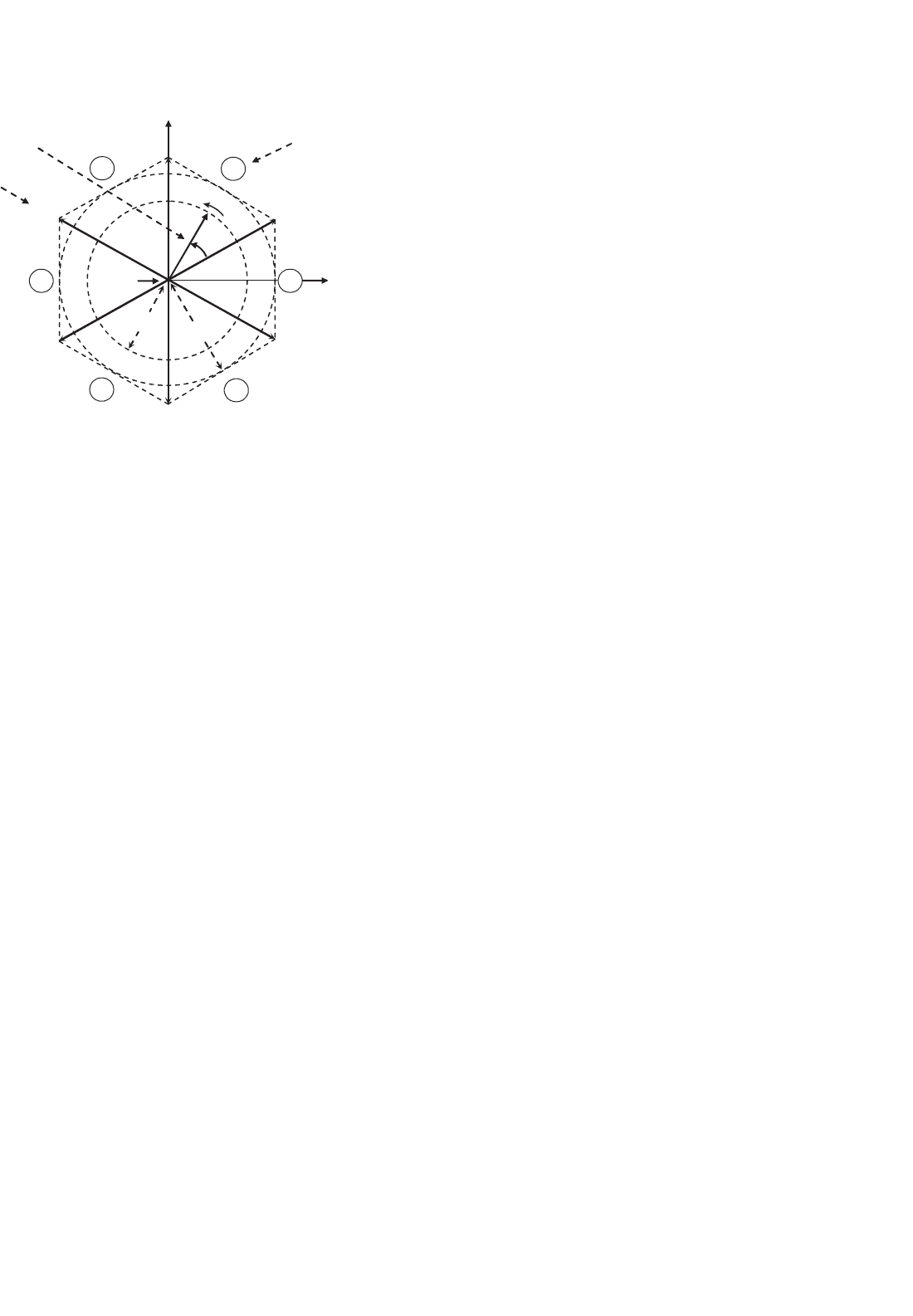
rotates at frequency ω (Fig. 15.20). Similarly, the SV transfor-
mation is applied to the line voltages of the eight states of the
15 Inverters 369
θ
6
1
2
3
4
5
sector number
modulating
vector
ω
state
α
β
1
v
c
= v
c
αβ
→
v
2
= v
i+1
→→
→
v
1
= v
i
→
v
6
→
v
5
→
v
4
→
v
3
→
v
7,8
→
v
c
ˆ
FIGURE 15.20 The space-vector representation.
VSI normalized with respect to v
i
(Table 15.3), which gener-
ates the eight space vectors (v
i
, i = 1, 2, ... , 8) in Fig. 15.20.
As expected, v
1
to v
6
are non-null line-voltage vectors and
v
7
and v
8
are null line-voltage vectors.
The objective of the SV technique is to approximate the
line-modulating signal space vector v
c
with the eight space
vectors (v
i
, i = 1, 2, ... , 8) available in VSIs. However, if the
modulating signal v
c
is laying between the arbitrary vectors v
i
and v
i+1
, only the nearest two non-zero vectors (v
i
and v
i+1
)
and one zero SV (v
z
=v
7
or v
8
) should be used. Thus, the
maximum load line voltage is maximized and the switching
frequency is minimized. To ensure that the generated voltage
in one sampling period T
s
(made up of the voltages provided
by the vectors v
i
, v
i+1
, and v
z
used during times T
i
, T
i+1
,
and T
z
) is on average equal to the vector v
c
the following
expression should hold:
v
c
·T
s
=v
i
·T
s
+v
i+1
·T
i+1
+v
z
·T
z
(15.38)
The solution of the real and imaginary parts of Eq. (15.37)
for a line-load voltage that features an amplitude restricted to
0 ≤ˆv
c
≤ 1 gives
T
i
= T
s
·ˆv
c
·sin(π/3 −θ) (15.39)
T
i+1
= T
s
·ˆv
c
·sin(θ) (15.40)
T
z
= T
s
−T
i
−T
i+1
(15.41)
The preceding expressions indicate that the maximum
fundamental line-voltage amplitude is unity as 0 ≤ θ ≤
π/3. This is an advantage over the SPWM technique which
achieves a
√
3/2 maximum fundamental line-voltage ampli-
tude in the linear operating region. Although, the space vector
modulation (SVM) technique selects the vectors to be used
and their respective on-times, the sequence in which they are
used, the selection of the zero space vector, and the normalized
sampled frequency remain undetermined.
For instance, if the modulating line-voltage vector is in
sector 1 (Fig. 15.20), the vectors v
1
, v
2
, and v
z
should be
used within a sampling period by intervals given by T
1
, T
2
,
and T
z
, respectively. The question that remains is whether
the sequence (i) v
1
−v
2
−v
z
, (ii) v
z
−v
1
−v
2
−v
z
,
(iii) v
z
−v
1
−v
2
−v
1
−v
z
, (iv) v
z
−v
1
−v
2
−v
z
−v
2
−v
1
−v
z
,
or any other sequence should actually be used. Finally, the
technique does not indicate whether v
z
should be v
7
, v
8
,ora
combination of both.
B. Space-vector Sequences and Zero Space-vector Selection
The sequence to be used should ensure load line-voltages that
feature quarter-wave symmetry in order to reduce unwanted
harmonics in their spectra (even harmonics). Additionally, the
zero SV selection should be done in order to reduce the switch-
ing frequency. Although there is not a systematic approach to
generate a SV sequence, a graphical representation shows that
the sequence v
i
, v
i+1
, v
z
(where v
z
is alternately chosen among
v
7
and v
8
) provides high performance in terms of minimizing
unwanted harmonics and reducing the switching frequency.
C. The Normalized Sampling Frequency
The normalized carrier frequency m
f
in three-phase carrier-
based PWM techniques is chosen to be an odd integer number
multiple of 3 (m
f
= 3 · n, n = 1, 3, 5, ...). Thus, it is possi-
ble to minimize parasitic or non-intrinsic harmonics in the
PWM waveforms. A similar approach can be used in the SVM
technique to minimize uncharacteristic harmonics. Hence, it is
found that the normalized sampling frequency f
sn
should be
an integer multiple of 6. This is due to the fact that in order to
produce symmetrical line voltages, all the sectors (a total of 6)
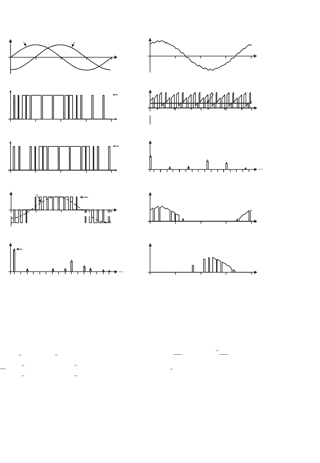
should be used equally in one period. As an example, Fig. 15.21
shows the relevant waveforms of a VSI SVM for f
sn
= 18 and
ˆv
c
= 0.8. Figure 15.21 confirms that the first set of relevant
harmonics in the load line voltage are at f
sn
which is also the
switching frequency.
15.3.6 DC Link Current in Three-phase VSIs
Due to the fact that the inverter is assumed to be loss-
less and constructed without storage energy components, the
instantaneous power balance indicates that
v
i
(t) · i
i
(t) = v
ab
(t) · i
a
(t) + v
bc
(t) · i
b
(t) + v
ca
(t) · i
c
(t)
(15.42)
where i
a
(t), i
b
(t), and i
c
(t) are the phase-load currents as
shown in Fig. 15.22. If the load is balanced and inductive, and
a relatively high switching frequency is used, the load currents
become nearly sinusoidal balanced waveforms. On the other
370 J. R. Espinoza
180 27090 360
ωt
v
ca
v
cβ
18090 360
ωt
i
oa
(a) (f)
180 270 90 360
ωt
0
S
1
on
180 27090 360
ωt
i
i
I
i
(b)
(g)
180 270 90 360
ωt
0
S
3
on
1579
f
f
o
3192331271151 131721 2925
i
i
(c)
(h)
18090
ωt
v
ab
v
ab1
v
i
180 27090 360
ωt
0
i
S
1
(d)
(i)
157931923312711511317212925
v
ab
f
f
o
0.8·v
i
180 27090 360
ωt
0
(e)
(j)
i
D
1
2702700 2700
0
270 360
0
FIGURE 15.21 The three-phase VSI. Ideal waveforms for space-vector modulation (ˆv
c
= 0.8, f
sn
= 18): (a) modulating signals; (b) switch S
1
state;
(c) switch S
3
state; (d) ac output voltage; (e) ac output voltage spectrum; (f) ac output current; (g) dc current; (h) dc current spectrum; (i) switch S
1
current; and (j) diode D
1
current.
hand, if the ac output voltages are considered sinusoidal and
the dc link voltage is assumed constant v
i
(t) = V
i
, Eq. (15.42)
can be simplified to
i
i
(t)=
1
V
i
√
2V
o1
sin(ωt)·
√
2I
o
sin(ωt −φ)
+
√
2V
o1
sin(ωt −120
◦
)·
√
2I
o
sin(ωt −120
◦
−φ)
+
√
2V
o1
sin(ωt −240
◦
)·
√
2I
o
sin(ωt −240
◦
−φ)
(15.43)
where V
o1
is the fundamental rms ac output line voltage, I
o
is
the rms load-phase current, and φ is an arbitrary inductive
load power factor. Hence, the dc link current expression can
be further simplified to
i
i
(t) = 3
V
o1
V
i
I
o
cos(φ) =
√
3
V
o1
V
i
I
l
cos(φ) (15.44)
where I
l
=
√
3I
o
is the rms load line current. The resulting
dc link current expression indicates that under harmonic-free
load voltages, only a clean dc current should be expected in
the dc bus and, compared to single-phase VSIs, there is no
presence of second harmonic. However, as the ac load line
voltages contain harmonics around the normalized sampling
15 Inverters 371
+
−
v
i
i
oa
+
−
v
ab
N
i
i
+
−
v
i
/2
+
−
v
i
/2
C
+
C
−
i
b
i
oc
+
−
v
bc
a
b
c
VSI
i
a
i
pb
i
c
FIGURE 15.22 Phase-load currents definition in a delta-connected
load.
frequency f
sn
, the dc link current will contain harmonics but
around f
sn
as shown in Fig. 15.21h.
15.3.7 Load-phase Voltages in Three-phase VSIs
The load is sometimes wye-connected and the phase-load volt-
ages v
an
, v
bn
, and v
cn
may be required (Fig. 15.23). To obtain
them, it should be considered that the line-voltage vector is
v
ab
v
bc
v
ca
=
v
an
−v
bn
v
bn
−v
cn
v
cn
−v
an
(15.45)
which can be written as a function of the phase-voltage vector
[v
an
v
bn
v
cn
]
T
as
v
ab
v
bc
v
ca
=
1 −10
01−1
−101
v
an
v
bn
v
cn
(15.46)
Expression (15.46) represents a linear system where the
unknown quantity is the vector [v
an
v
bn
v
cn
]
T
. Unfortunately,
+
−
v
i
i
oa
+
+
+v
cn
v
an
v
bn
+
−
−
v
ab
N
i
i
+
−
v
i
/2
+
−
v
i
/2
C
+
C
−
i
ob
i
oc
+
−
v
bc
a
b
c
VSI
n
FIGURE 15.23 Phase-load voltages definition in a wye-connected load.
18090
ωt
v
ab
v
ab1
v
i
180
ωt
v
an
v
an1
2v
i
/3
(a) (b)
270270 3603600
270
2709090 3603600
270 3600
27090 3600
FIGURE 15.24 The three-phase VSI. Line- and phase-load voltages: (a) line-load voltage v
ab
; and (b) phase-load voltage v
an
.
the system is singular as the rows add up to zero (line volt-
ages add up to zero), therefore, the phase-load voltages cannot
be obtained by matrix inversion. However, if the phase-load
voltages add up to zero, Eq. (15.46) can be rewritten as
v
ab
v
bc
0
=
1 −10
01−1
111
v
an
v
bn
v
cn
(15.47)
which is not singular and hence,
v
an
v
bn
v
cn
=
1 −10
01−1
111
−1
v
ab
v
bc
0
=
1
3
211
−111
−1 −21
v
ab
v
bc
0
(15.48)
that can be further simplified to
v
an
v
bn
v
cn
=
1
3
21
−11
−1 −2
v
ab
v
bc
(15.49)
The final expression for the phase-load voltages is only a
function of v
ab
and v
bc
, which is due to fact that the last row
in Eq. (15.46) is chosen to be only ones. Figure 15.24 shows
the line- and phase-voltages obtained using Eq. (15.49).
15.4 Current Source Inverters
The main objective of these static power converters is to
produce an ac output current waveforms from a dc current
power supply. For sinusoidal ac outputs, its magnitude, fre-
quency, and phase should be controllable. Due to the fact that
the ac line currents i
oa
, i
ob
, and i
oc
(Fig. 15.25) feature high
di/dt, a capacitive filter should be connected at the ac ter-
minals in inductive load applications (such as ASDs). Thus,
nearly sinusoidal load voltages are generated that justifies the
use of these topologies in medium-voltage industrial appli-
cations, where high-quality voltage waveforms are required.
Although single-phase CSIs can in the same way as three-phase
CSIs topologies, be developed under similar principles, only
three-phase applications are of practical use and are analyzed
below.
372 J. R. Espinoza
i
i
S
1
a
S
4
D
1
D
4
S
3
b
S
6
D
3
D
6
i
oa
+
−
v
ab
S
5
c
S
2
D
5
D
2
+
−
v
i
C
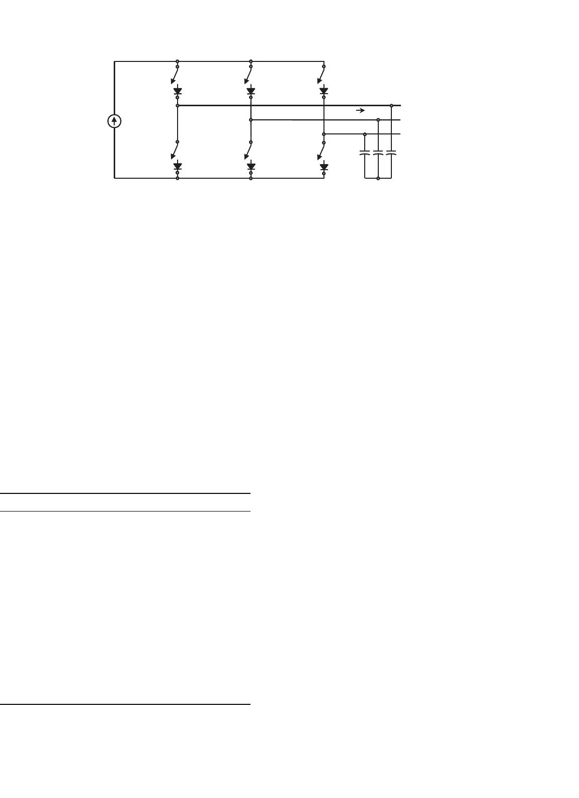
FIGURE 15.25 Three-phase CSI topology.
In order to properly gate the power switches of a three-phase
CSI, two main constraints must always be met: (a) the ac side
is mainly capacitive, thus, it must not be short-circuited; this
implies that, at most one top switch (1, 3, or 5 (Fig. 15.25)) and
one bottom switch (4, 6, or 2 (Fig. 15.25)) should be closed at
any time; and (b) the dc bus is of the current-source type and
thus it cannot be opened; therefore, there must be at least one
top switch (1, 3, or 5) and one bottom switch (4, 6, or 2) closed
at all times. Note that both constraints can be summarized by
stating that at any time, only one top switch and one bottom
switch must be closed.
There are nine valid states in three-phase CSIs. The states 7,
8, and 9 (Table 15.4) produce zero ac line currents. In this case,
the dc link current freewheels through either the switches S
1
and S
4
, switches S
3
and S
6
, or switches S
5
and S
2
. The remain-
ing states (1 to 6 in Table 15.4) produce non-zero ac output
line currents. In order to generate a given set of ac line current
waveforms, the inverter must move from one state to another.
Thus, the resulting line currents consist of discrete values of
TABLE 15.4 Valid switch states for a three-phase CSI
State State # i
oa
i
ob
i
oc
Space vector
S
1
and S
2
are on and S
3
, S
4
,
S
5
, and S
6
are off
1 i
i
0 −i
i
i
1
= 1 + j0.577
S
2
and S
3
are on and S
4
, S
5
,
S
6
, and S
1
are off
20i
i
−i
i
i
2
= j1.155
S
3
and S
4
are on and S
5
, S
6
,
S
1
, and S
2
are off
3 −i
i
i
i
0
i
3
=−1 + j0.577
S
4
and S
5
are on and S
6
, S
1
,
S
2
, and S
3
are off
4 −i
i
0 i
i
i
4
=−1 − j0.577
S
5
and S
6
are on and S
1
, S
2
,
S
3
, and S
4
are off
50−i
i
i
i
i
5
=−j1.155
S
6
and S
1
are on and S
2
, S
3
,
S
4
, and S
5
are off
6 i
i
−i
i
0
i
6
= 1 − j0.577
S
1
and S
4
are on and S
2
, S
3
,
S
5
, and S
6
are off
7 000
i
7
= 0
S
3
and S
6
are on and S
1
, S
2
,
S
4
, and S
5
are off
8 000
i
8
= 0
S
5
and S
2
are on and S
6
, S
1
,
S
3
, and S
4
are off
9 000
i
9
= 0
current, which are i
i
,0,and−i
i
. The selection of the states in
order to generate the given waveforms is done by the modu-
lating technique that should ensure the use of only the valid
states.
There are several modulating techniques that deal with
the special requirements of CSIs and can be implemented
online. These techniques are classified into three categories:
(a) the carrier-based; (b) the SHE-based; and (c) the SV-based
techniques. Although they are different, they generate gat-
ing signals that satisfy the special requirements of CSIs. To
simplify the analysis, a constant dc link-current source is
considered (i
i
= I
i
).
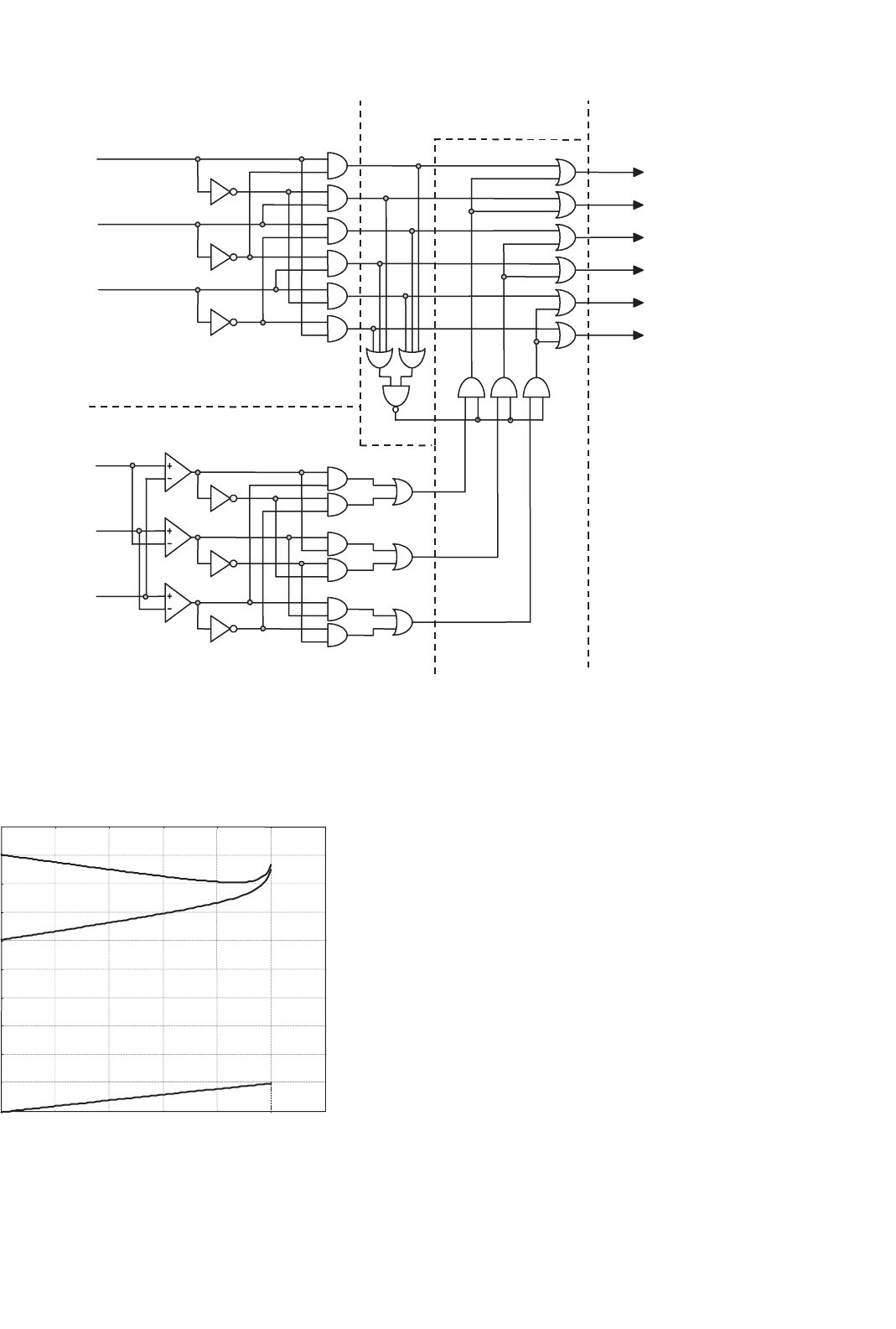
15.4.1 Carrier-based PWM Techniques in CSIs
It has been shown that the carrier-based PWM techniques that
were initially developed for three-phase VSIs can be extended
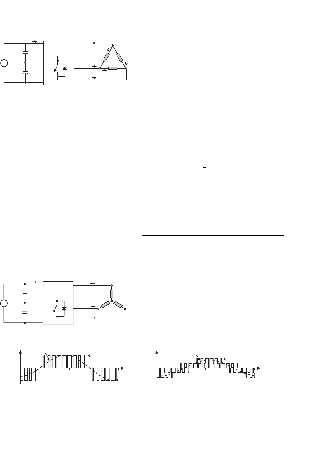
to three-phase CSIs. The circuit shown in Fig. 15.26 obtains
the gating pattern for a CSI from the gating pattern developed
for a VSI. As a result, the line current appears to be identical
to the line voltage in a VSI for similar carrier and modulating
signals.
It is composed of a switching pulse generator,ashorting pulse
generator,ashorting pulse distributor, and a switching and short-
ing pulse combinator. The circuit basically produces the gating
signals (s = [s
1
...s
6
]
T
) according to a carrier i
and three
modulating signals i
abc
c
=[i
ca
i
cb
i
ca
]
T
. Therefore, any set of
modulating signals which when combined result in a sinu-
soidal line-to-line set of signals, will satisfy the requirement for
a sinusoidal line current pattern. Examples of such a modu-
lating signals are the standard sinusoidal, sinusoidal with third
harmonic injection, trapezoidal, and deadband waveforms.
The first component of this stage (Fig. 15.26) is the switch-
ing pulse generator, where the signals s
123
a
are generated
according to:
s
123
a
=
HIGH = 1 if i
abc
c
> v
c
LOW = 0 otherwise
(15.50)
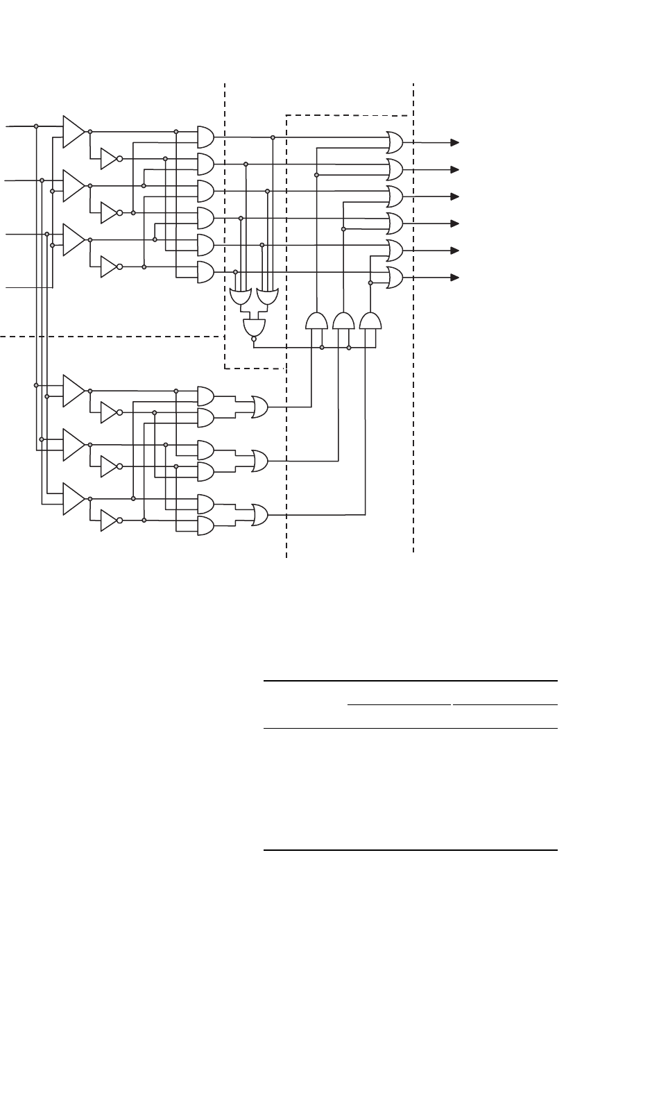
15 Inverters 373
S
1
S
4
S
3
S
6
S
5
Switching pulse generator Shorting pulse generator
Shorting pulse distributor
Switching and
shorting pulse
combinator
S
a1
S
d
i
D
i
ca
i
cb
i
cc
S
a2
S
a3
S
c3
S
c4
S
c1
S
c6
S
c5
S
c2
S
b1
S
b2
S
b3
S
2
gating
signals
S
f1
S
f 2
S
f 3
+
+
+
−
−
−
+
−
+
−
+
−
S
e2
S
e1
S
e3
FIGURE 15.26 The three-phase CSI. Gating pattern generator for analog on-line carrier-based PWM.
The outputs of the switching pulse generator are the signals
s
c
, which are basically the gating signals of the CSI without
the shorting pulses. These are necessary to freewheel the dc
link current i
i
when zero ac output currents are required.
Table 15.5 shows the truth table of s
c
for all combinations
of their inputs s
123
a
. It can be clearly seen that at most one top
switch and one bottom switch is on, which satisfies the first
constraint of the gating signals as stated before.
In order to satisfy the second constraint, the shorting
pulse (s
d
=1) (s
d
= 1) is generated (shorting pulse generator
(Fig. 15.26)) the top switches (s
c1
= s
c3
= s
c5
= 0) or none
of the bottom switches (s
c4
= s
c6
= s
c2
= 0) are gated. Then,
this pulse is added (using OR gates) to only one leg of the CSI
(either to the switches 1 and 4, 3 and 6, or 5 and 2) by means
of the switching and shorting pulse combinator (Fig. 15.26). The
signals generated by the shorting pulse generator s
123
e
ensure
that: (a) only one leg of the CSI is shorted, as only one of the
signals is HIGH at any time; and (b) there is an even distri-
bution of the shorting pulse, as s
123
e
is high for 120
◦
in each
period. This ensures that the rms currents are equal in all legs.
TABLE 15.5 Truth table for the switching pulse generator
stage (Fig. 15.26)
s
a1
s
a2
s
a3
Top switches Bottom switches
s
c1
s
c3
s
c5
s
c4
s
c6
s
c2
0000 0 0 0 0 0
0010 0 1 0 1 0
0100 1 0 1 0 0
0110 0 1 1 0 0
1001 0 0 0 0 1
1011 0 0 0 1 0
1100 1 0 0 0 1
1110 0 0 0 0 0
Figure 15.27 shows the relevant waveforms if a trian-
gular carrier i
and sinusoidal modulating signals i
abc
c
are
used in combination with the gating pattern generator cir-
cuit (Fig. 15.26); this is SPWM in CSIs. It can be observed
that some of the waveforms (Fig. 15.27) are identical to those
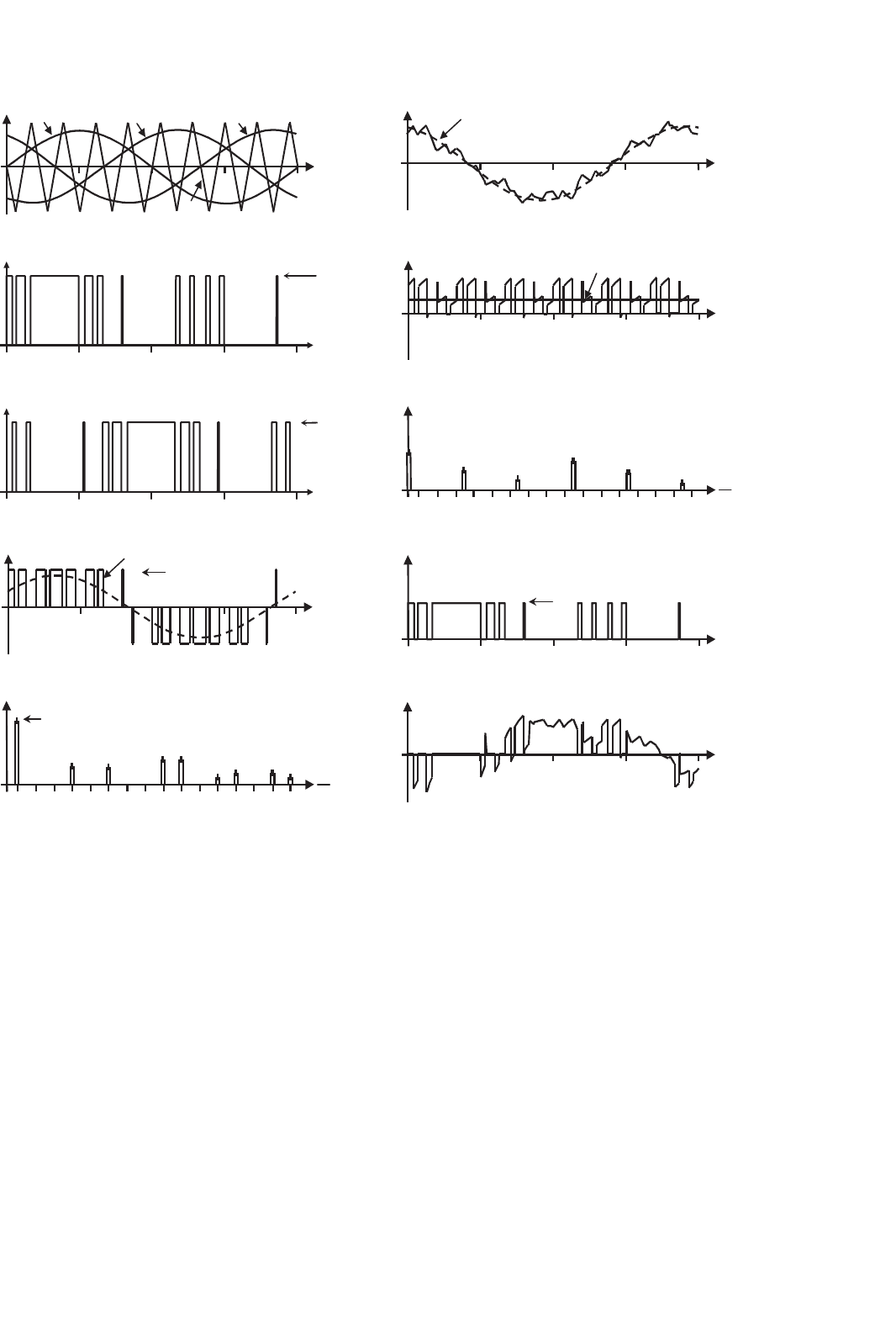
374 J. R. Espinoza
360
ωt
i
ca
i
cb
i
cc
i
D
180 270 360
ωt
v
ab
v
ab1
(a)
(f)
180 270 90 360
ωt
0
S
1
on
180 27090 360
ωt
v
i
V
i
(b)
(g)
180 270 90 360
ωt
0
S
3
on
1579
f
f
o
31923312711511317212925
v
i
(c)
(h)
90 360
ωt
i
oa
i
oa1
i
i
180 27090 360
ωt
0
i
S
1
i
i
(d)
(i)
15793192331271151 131721 2925
i
oa
f
f
o
0.8·0.866·i
i
180 270
ωt
(e)
(j)
v
S
1
0
0
180
180
270270
9090
90900
180
180 270270
9090 360360
0
0
0
180
270
90
900
180 270
90 360
0
FIGURE 15.27 The three-phase CSI. Ideal waveforms for the SPWM (m
a
= 0.8, m
f
= 9): (a) carrier and modulating signals; (b) switch S
1
state;
(c) switch S
3
state; (d) ac output current; (e) ac output current spectrum; (f) ac output voltage; (g) dc voltage; (h) dc voltage spectrum; (i) switch S
1
current; and (j) switch S
1
voltage.
obtained in three-phase VSIs, where a SPWM technique is used
(Fig. 15.15). Specifically: (i) the load line voltage (Fig. 15.15d)
in the VSI is identical to the load line current (Fig. 15.27d)
in the CSI; and (ii) the dc link current (Fig. 15.15g) in
the VSI is identical to the dc link voltage (Fig. 15.27g) in
the CSI.
This brings up the duality issue between both the topolo-
gies when similar modulation approaches are used. Therefore,
for odd multiples of 3 values of the normalized carrier fre-
quency m
f
, the harmonics in the ac output current appear
at normalized frequencies f
h
centered around m
f
and its
multiples, specifically, at
h = lm
f
±kl= 1, 2, ... (15.51)
where l = 1, 3, 5, ... for k = 2, 4, 6, ... and l = 2, 4, ... for
k = 1, 5, 7, ...such that h is not a multiple of 3. Therefore, the
harmonics will be at m
f
±2, m
f
±4, ...,2m
f
±1, 2m
f
±5, ...,
3m
f
±2, 3m
f
±4, ...,4m
f
±1, 4m
f
±5, .... For nearly sinu-
soidal ac load voltages, the harmonics in the dc link voltage
are at frequencies given by
h = lm
f
±k ± 1 l = 1, 2, ... (15.52)
15 Inverters 375
where l = 0, 2, 4, ... for k = 1, 5, 7, ... and l = 1, 3, 5, ...
for k = 2, 4, 6, ... such that h = l ·m
f
± k is positive and
not a multiple of 3. For instance, Fig. 15.27h shows the sixth
harmonic (h = 6), which is due to h = 1 · 9 − 2 − 1 = 6.
Identical conclusions can be drawn for the small and large
values of m
f
in the same way as for three-phase VSI config-
urations. Thus, the maximum amplitude of the fundamental
ac output line current is
ˆ
i
oa1
=
√
3i
i
/2 and therefore one can
write
ˆ
i
oa1
= m
a
√
3
2
i
i
0 < m
a
≤ 1 (15.53)
ωt
i
ca
i
D
i
cc
i
cb
180 27090 360
ωt
0
S
d
on
(a) (f)
180 27090 360
ωt
0
S
a1
S
c1
on
180 27090 360
ωt
0
S
f
1
on
(b) (g)
180 27090 360
ωt
0
on
180 27090 360
ωt
0
S
1
on
(c) (h)
180 27090 360
ωt
0
on
90 360
ωt
i
oa
i
oa1
i
i
(d) (i)
180 27090 360
ωt
0
on
15793 19 23 31271151 131721 2925
i
oa
f
f
o
0.8·0.866·i
i
(e) (j)
S
b1
S
e1
0
180
180 2702709090 360360
180180 2702700
180 27090 360
180 270
FIGURE 15.28 Gating pattern generator. Waveforms for third and ninth harmonic injection PWM (m
a
= 0.8, m
f
= 15): signals as described in
Fig. 15.26.
To further increase the amplitude of the load current, the
overmodulation approach can be used. In this region, the
fundamental line currents range in
√
3
2
i
i
<
ˆ
i
oa1
=
ˆ
i
ob1
=
ˆ
i
oc1
<
4
π
√
3
2
i
i
(15.54)
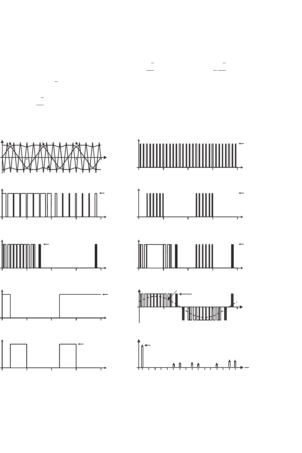
To further test the gating signal generator circuit
(Fig. 15.26), a sinusoidal set with third and ninth harmonic
injection modulating signals are used. Figure 15.28 shows the
relevant waveforms.
376 J. R. Espinoza
S
1
180 27090 360
ωt
0
on
27090 360
ω
t
i
oa
i
oa1
i
i
(a)
(c)
S
3
180 27090 360
ωt
0
on
1573 19 23 31271151 9 13 17 21 2925
i
oa
f
f
o
1.1i
i
(
b
)(
d
)
180
180
0 1800
FIGURE 15.29 The three-phase CSI. Square-wave operation: (a) switch S
1
state; (b) switch S
3
state; (c) ac output current; and (d) ac output current
spectrum.
15.4.2 Square-wave Operation of
Three-phase CSIs
As in VSIs, large values of m
a
in the SPWM technique lead to
full overmodulation. This is known as square-wave operation.
Figure 15.29 depicts this operating mode in a three-phase CSI,
where the power valves are on for 120
◦
. As presumed, the CSI
cannot control the load current except by means of the dc link
current i
i
. This is due to the fact that the fundamental ac line
current expression is
ˆ
i
oa1
=
4
π
√
3
2
i
i
(15.55)
The ac line current contains the harmonics f
h
, where h =
6 · k ± 1(k = 1, 2, 3, ...), and they feature amplitudes that is
inversely proportional to their harmonic order (Fig. 15.29d).
Thus,
ˆ
i
oah
=
1
h
4
π
√
3
2
i
i
(15.56)
The duality issue among both the three-phase VSI and CSI
should be noted especially in terms of the line-load waveforms.
The line-load voltage produced by a VSI is identical to the load
line current produced by the CSI when both are modulated
using identical techniques. The next section will show that this
also holds for SHE-based techniques.
15.4.3 Selective Harmonic Elimination in
Three-phase CSIs
The SHE-based modulating techniques in VSIs define the
gating signals such that a given number of harmonics are
eliminated and the fundamental phase-voltage amplitude is
controlled. If the required line output voltages are balanced
and 120
◦
out-of-phase, the chopping angles are used to elim-
inate only the harmonics at frequencies h = 5, 7, 11, 13, ... as
required.
The circuit shown in Fig. 15.30 uses the gating signals s
123
a
developed for a VSI and a set of synchronizing signals i
abc
c
to
obtain the gating signals s for a CSI. The synchronizing signals
i
abc
c
are sinusoidal balanced waveforms that are synchronized
with the signals s
123
a
in order to symmetrically distribute the
shorting pulse and thus generate symmetrical gating patterns.
The circuit ensures line current waveforms as the line voltages
in a VSI. Therefore, any arbitrary number of harmonics can be
eliminated and the fundamental line current can be controlled
in CSIs. Moreover, the same chopping angles obtained for VSIs
can be used in CSIs.
For instance, to eliminate the fifth and seventh harmonics,
the chopping angles are shown in Fig. 15.31, which are iden-
tical to that obtained for a VSI using Eq. (15.9). Figure 15.32
shows that the line current does not contain the fifth and the
seventh harmonics as expected. Hence, any number of har-
monics can be eliminated in three-phase CSIs by means of the
circuit (Fig. 15.30) without the hassle of how to satisfy the
gating signal constrains.
15.4.4 Space-vector-based Modulating
Techniques in CSIs
The objective of the SV-based modulating technique is to gen-
erate PWM load line currents that are on average equal to
given load line currents. This is done digitally in each sampling
period by properly selecting the switch states from the valid
ones of the CSI (Table 15.4) and the proper calculation of the
period of times they are used. As in VSIs, the selection and time
calculations are based upon the space-vector transformation.
15 Inverters 377
S
1
S
4
S
3
S
6
S
5
Switching pulse generator
Shorting pulse generator
Shorting pulse distributor
Switching and
shorting pulse
combinator
S
a1
S
d
i
ca
i
cb
i
cc
S
a2
S
a3
S
c3
S
c4
S
c1
S
c6
S
c5
S
c2
S
e1
S
e2
S
e3
S
b1
S
b2
S
b3
S
2
gating
signals
S
f 1
S
f 2
S
f 3
FIGURE 15.30 The three-phase CSI. Gating pattern generator for SHE PWM techniques.
i
oa1
/i
i
ˆ
0 0.2 0.4 0.6 0.8 1.0
0°
10°
20°
30°
40°
50°
60°
70°
80°
90°
100°
α
1
α
3
α
2
FIGURE 15.31 Chopping angles for SHE and fundamental current
control in three-phase CSIs: fifth and seventh harmonic elimination.
A. Space-vector Transformation in CSIs
Similarly to VSIs, the vector of three-phase line-modulating
signals i
abc
c
=[i
ca
i
cb
i
cc
]
T
can be represented by the com-
plex vector
i
c
= i
ab
c
=[i
cα
i
cβ
]
T
by means of Eqs. (15.36)
and (15.37). For three-phase balanced sinusoidal modulating
waveforms, which feature an amplitude
ˆ
i
c
and an angular fre-
quency ω, the resulting modulating signals complex vector
i
c
= i
ab
c
becomes a vector of fixed module
ˆ
i
c
, which rotates at
frequency ω (Fig. 15.33). Similarly, the SV transformation is
applied to the line currents of the nine states of the CSI nor-
malized with respect to i
i
, which generates nine space vectors
(
i
i
, i = 1, 2, ..., 9 in Fig. 15.33). As expected,
i
1
to
i
6
are non-
null line current vectors and
i
7
,
i
8
, and
i
9
are null line current
vectors.
The SV technique approximates the line-modulating sig-
nal space vector
i
c
by using the nine space vectors (
i
i
, i =
1, 2, ..., 9) available in CSIs. If the modulating signal vector
i
c
is between the arbitrary vectors
i
i
and
i
i+1
, then
i
i
and
i
i+1
combined with one zero SV (
i
z
=
i
7
or
i
8
or
i
9
) should be
used to generate
i
c
. To ensure that the generated current in