Power electronic handbook
Подождите немного. Документ загружается.

378 J. R. Espinoza
S
a1
180 270 90 360
ωt
0
α
1
α
2
α
3
90 360
ωt
i
oa
i
oa1
i
i
(a)
(c)
S
1
180 270 90 360
ωt
0
on
15793 19 23 312711511317212925
i
oa
f
f
o
0.8·i
i
(b) (d)
180
180 2702700 180 2700
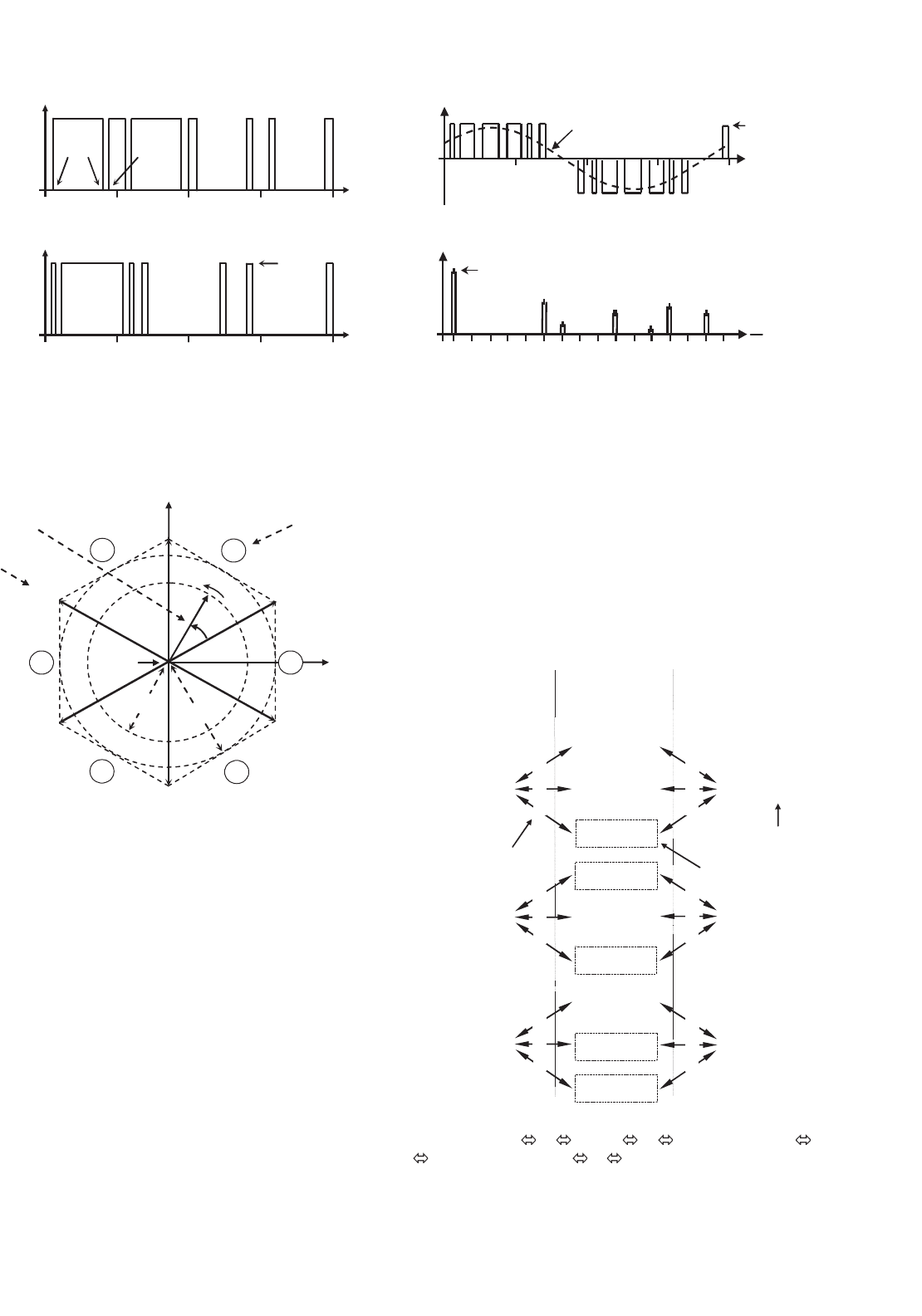
FIGURE 15.32 The three-phase CSI. Ideal waveforms for the SHE technique: (a) VSI gating pattern for fifth and seventh harmonic elimina-
tion; (b) CSI gating pattern for fifth and seventh harmonic elimination; (c) line current i
oa
for fifth and seventh harmonic elimination; and
(d) spectrum of (c).
θ
6
1
2
3
4
5
sector number
modulating
vector
ω
state
α
β
1
i
c
ˆ
i
5
→
i
c
= i
c
αβ
→→
i
3
→
i
4
→
2
i
=
1i+
i
→→
i
1
= i
i
→→
i
7,8,9
→
i
6
→
FIGURE 15.33 The space-vector representation in CSIs.
one sampling period T
s
(made up of the currents provided by
the vectors
i
i
,
i
i+1
, and
i
z
used during times T
i
, T
i+1
, and T
z
)
is on average equal to the vector
i
c
, the following expressions
should hold:
T
i
= T
s
·
ˆ
i
c
·sin(π/3 −θ) (15.57)
T
i+1
= T
s
·
ˆ
i
c
·sin(θ) (15.58)
T
z
= T
s
−T
i
−T
i+1
(15.59)
where 0 ≤
ˆ
i
c
≤ 1. Although, the SVM technique selects the
vectors to be used and their respective on-times, the sequence
in which they are used, the selection of the zero space vector,
and the normalized sampled frequency remain undetermined.
B. Space-vector Sequences and Zero Space-vector Selection
Although there is no systematic approach to generate a SV
sequence, a graphical representation shows that the sequence
i
i
,
i
i+1
,
i
z
(where the chosen
i
z
depends upon the sector)
provides high performance in terms of minimizing unwanted
harmonics and reducing the switching frequency. To obtain
the zero SV that minimizes the switching frequency, it is
assumed that I
c
is in Sector ➁. Then Fig. 15.34 shows all
Initial state
Final state
Possible
Zero Vector
(a)
(b)
(c)
2
1
1
1
2
1
2
1
1
1
2
1
1
2
1
2
1
1
number of
commutations
on switches
minimum number
of commutations
i
2
= {2, 3}
→
i
1
= {1, 2}
→
i
1
= {1, 2}
→
i
7
= {1, 4}
→
i
8
= {3, 6}
→
i
9
= {5, 2}
→
i
7
= {1, 4}
→
i
8
= {3, 6}
→
i
9
= {5, 2}
→
i
7
= {1, 4}
→
i
8
= {3, 6}
→
i
9
= {5, 2}
→
i
2
= {2, 3}
→
i
2
= {2, 3}
→
i
1
= {1, 2}
→
FIGURE 15.34 Possible state transitions in Sector ➁ involving a zero
SV: (a) transition:
i
1
i
z
i
2
or
i
2
i
z
i
1
; (b) transition:
i
1
i
z
i
1
; and (c) transition:
i
2
i
z
i
2
.

15 Inverters 379
TABLE 15.6 Zero SV for minimum switching
frequency in CSI and sequence
i
i
,
i
i+1
,
i
z
Sector
i
i
i
i+1
i
z
➀
i
6
i
1
i
7
➁
i
1
i
2
i
9
➂
i
2
i
3
i
8
➃
i
3
i
4
i
7
➄
i
4
i
5
i
9
➅
i
5
i
6
i
8
the possible transitions that could be found in Sector ➁.
It can be seen that the zero vector
i
9
should be chosen to
minimize the switching frequency. Table 15.6 gives a sum-
mary of the zero space vector to be used in each sector in
order to minimize the switching frequency. However, should
be noted that Table 15.6 is valid only for the sequence
i
i
,
i
i+1
,
i
z
. Another sequence will require reformulating the zero
space-vector selection algorithm.
C. The Normalized Sampling Frequency
As in VSIs modulated by a SV approach, the normalized sam-
pling frequency f
sn
should be an integer multiple of 6 to min-
imize uncharacteristic harmonics. As an example, Fig. 15.35
shows the relevant waveforms of a CSI SVM for f
sn
= 18 and
ˆ
i
c
= 0.8. Figure 15.35 also shows that the first set of relevant
harmonics load line current are at f
sn
.
15.4.5 DC Link Voltage in Three-phase CSIs
An instantaneous power balance indicates that
v
i
(t) · i
i
(t) = v
an
(t) · i
oa
(t) + v
bn
(t) · i
ob
(t) + v
cn
(t) · i
oc
(t)
(15.60)
where v
an
(t), v
bn
(t), and v
cn
(t) are the phase filter voltages
as shown in Fig. 15.36. If the filter is large enough and a
relatively high switching frequency is used, the phase voltages
become nearly sinusoidal balanced waveforms. On the other
hand, if the ac output currents are considered sinusoidal and
the dc link current is assumed constant i
i
(t) = I
i
, Eq. (15.60)
can be simplified to
v
i
(t)=
1
I
i
√
2V
on
sin(ωt)·
√
2I
o1
sin(ωt −φ)
+
√
2V
on
sin(ωt −120
◦
)·
√
2I
o1
sin(ωt −120
◦
−φ)
+
√
2V
on
sin(ωt −240
◦
)·
√
2I
o1
sin(ωt −240
◦
−φ)
(15.61)
where V
on
is the rms ac output phase voltage, I
o1
is the rms
fundamental line current, and φ is an arbitrary filter-load
angle. Hence, the dc link voltage expression can be further
simplified to the following:
v
i
(t) = 3
I
o1
I
i
V
on
cos(φ) =
√
3
I
o1
I
i
V
o
cos(φ) (15.62)
where V
o
=
√
3V
on
is the rms load line voltage. The resulting
dc link voltage expression indicates that the first line-current
harmonic I
o1
generates a clean dc current. However, as the
load line currents contain harmonics around the normalized
sampling frequency f
sn
, the dc link current will contain har-
monics but around f
sn
as shown in Fig. 15.35h. Similarly, in
carrier-based PWM techniques, the dc link current will contain
harmonics around the carrier frequency m
f
(Fig. 15.27).
In practical implementations, a CSI requires a dc current
source that should behave as a constant (as required by PWM
CSIs) or variable (as square-wave CSIs) current source. Such
current sources should be implemented as separate units and
they are described earlier in this book.
15.5 Closed-loop Operation of Inverters
Inverters generate variable ac waveforms from a dc power sup-
ply to feed, for instance, ASDs. As the load conditions usually
change, the ac waveforms should be adjusted to these new con-
ditions. Also, as the dc power supplies are not ideal and the
dc quantities are not fixed, the inverter should compensate for
such variations. Such adjustments can be done automatically
by means of a closed-loop approach. Inverters also provide
an alternative to changing the load operating conditions (i.e.
speed in an ASD).
There are two alternatives for closed-loop operation the
feedback and the feedforward approaches. It is known that
the feedback approach can compensate for both the pertur-
bations (dc power variations) and the load variations (load
torque changes). However, the feedforward strategy is more
effective in mitigating perturbations as it prevents its negative
effects at the load side. These cause-effect issues are analyzed in
three-phase inverters in the following, although similar results
are obtained for single-phase VSIs.
15.5.1 Feedforward Techniques in Voltage
Source Inverters
The dc link bus voltage in VSIs is usually considered a constant
voltage source v
i
. Unfortunately, and due to the fact that most
practical applications generate the dc bus voltage by means of
a diode rectifier (Fig. 15.37), the dc bus voltage contains low-
order harmonics such as the sixth, twelfth, ...(due to six-pulse
380 J. R. Espinoza
180 270
ωt
i
ca
i
cβ
18090 360
ω
t
v
ab
i
oa1
(a) (f)
180 27090 360
ωt
0
S
1
on
180 27090 360
ωt
v
i
V
i
(b)
(g)
180 27090 360
ωt
0
S
3
on
1579
f
f
o
31923312711511317212925
v
i
(c) (h)
90 360
ωt
i
oa
i
oa1
i
i
180 27090 360
ωt
0
i
S
1
i
i
(d)
(i)
157931923312711511317212925
i
oa
f
f
o
0.8·i
i
180 27090
ωt
(e)
(j)
v
S
1
9090 360360
2702700
180
180 2702700
360360
90 360
2700
180 2700
360
00
00
FIGURE 15.35 The three-phase CSI. Ideal waveforms for space-vector modulation (
ˆ
i
c
= 0.8, f
sn
= 18): (a) modulating signals; (b) switch S
1
state;
(c) switch S
3
state; (d) ac output current; (e) ac output current spectrum; (f) ac output voltage; (g) dc voltage; (h) dc voltage spectrum; (i) switch S
1
current; and (j) switch S
1
voltage.
i
oa
+
−
v
ab
i
ob
i
oc
+
−
v
bc
a
b
c
CSI
v
an
v
bn
v
cn
+
−
+
+
n
i
i
+
−
v
i
i
la
i
lc
i
lb
FIGURE 15.36 Phase-voltage definition in a wye-connected filter.
diode rectifiers), and the second if the ac voltage supply
features an unbalance, which is usually the case. Additionally, if
the three-phase load is unbalanced, as in UPS applications, the
dc input current in the inverter i
i
also contains the second har-
monic, which in turn contributes to the generation of a second
voltage harmonic in the dc bus.
The basic principle of feedforward approaches is to sense
the perturbation and then modify the input in order to com-
pensate for its effect. In this case, the dc link voltage should
be sensed and the modulating technique should accordingly
be modified. The fundamental ab line voltage in a VSI SPWM
15 Inverters 381
v
as
i
oa
+
−
v
ab
N
i
i
+
−
v
i
/2
+
−
C
+
C
−
i
ob
i
oc
+
−
v
bc
a
b
c
VSI
v
an
v
bn
v
cn
+
−
+
+
n
Diode
Rectifier
i
sa
v
bs
v
cs
v
i
/2
FIGURE 15.37 Three-phase VSI topology with a diode-based front-end rectifier.
can be written as
v
ab1
(t) =
v
ca1
(t)
ˆv
−
v
cb1
(t)
ˆv
√
3
2
v
i
(t) ˆv
> ˆv
ca1
, ˆv
cb1
(15.63)
where ˆv
is the carrier signal peak, ˆv
ca1
and ˆv
cb1
are the mod-
ulating signal peaks, and v
ca
(t) and v
ca
(t) are the modulating
signals. If the dc bus voltage v
i
varies around a nominal V
i
value, then the fundamental line voltage varies proportionally;
however, if the carrier signal peak ˆv
is redefined as
ˆv
=ˆv
m
v
i
(t)
V
i
(15.64)
where ˆv
m
is the carrier signal peak (Fig. 15.38), then the
resulting fundamental ab line voltage in a VSI SPWM is
v
ab1
(t) =
v
ca1
(t)
ˆv
m
−
v
cb1
(t)
ˆv
m
√
3
2
V
i
(15.65)
where, clearly, the result does not depend upon the variations
of the dc bus voltage.
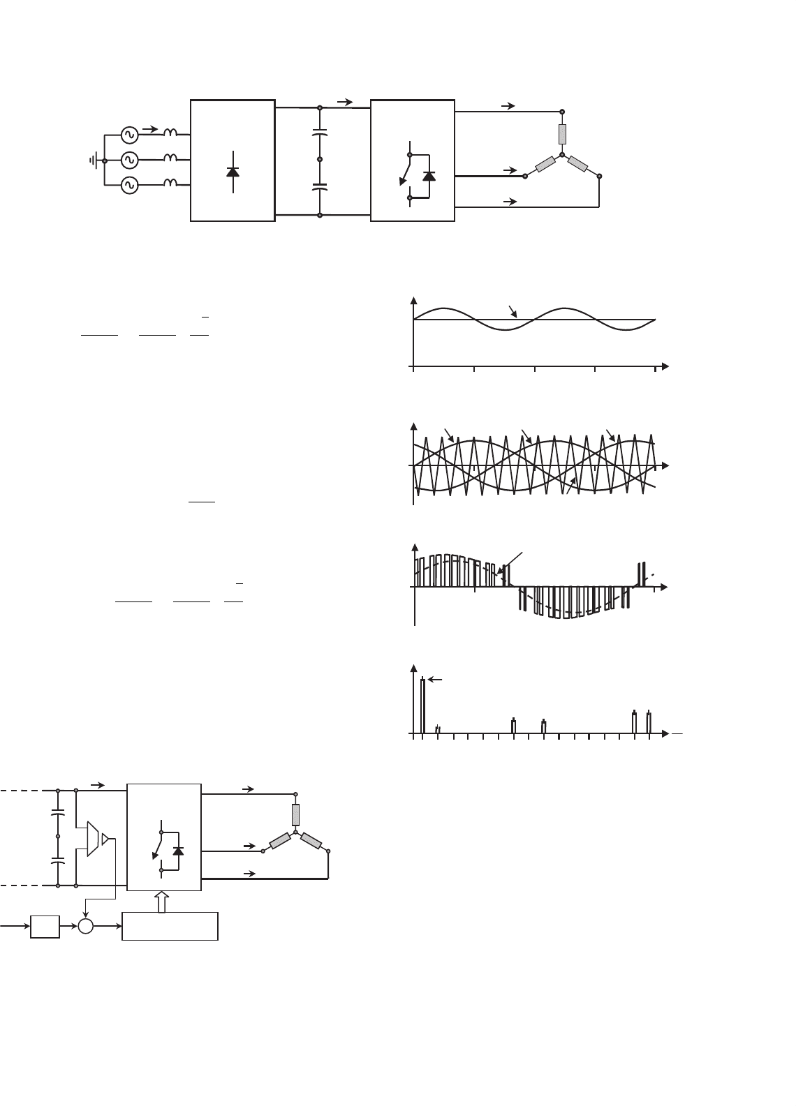
Figure 15.39 shows the waveforms generated by the SPWM
under a severe dc bus voltage variation (a second harmonic has
been added manually to a constant V
i
). As a consequence, the
ac line voltage generated by the VSI is distorted as it contains
i
oa
+
−
v
ab
N
i
i
+
−
+
−
C
+
C
−
i
ob
i
oc
+
−
v
bc
a
b
c
VSI
v
an
v
bn
v
cn
+
−
+
+
n
Carrier-based
Modulation Technique
S
1-6
v
∆
v
i
x
1/V
i
v
∆m
FIGURE 15.38 The three-phase VSI. Feedforward control technique to
reject dc bus voltage variations.
180 27090 360
ωt
0
v
i
V
i
(a)
360
ωt
(b)
90 360
ωt
v
ab
v
ab1
(c)
157931923312711511317212925
v
ab
f
f
o
0.8·0.866·v
i
(d)
v
ca
v
cb
v
cc
v
D
180180 2702709090
180180 270270
180 27090
180 27000
FIGURE 15.39 The three-phase VSI. Waveforms for regular SPWM
(m
a
= 0.8, m
f
= 9): (a) dc bus voltage; (b) carrier and modulating
signals; (c) ac output voltage; and (d) ac output voltage spectrum.
low-order harmonics (Fig. 15.39e). These operating condi-
tions may not be acceptable in standard applications such as
ASDs because the load will draw distorted three-phase cur-
rents as well. The feedforward loop performance is illustrated
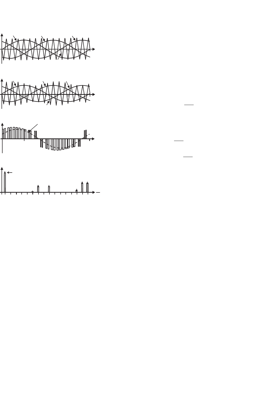
in Fig. 15.40. As expected, the carrier signal is modified so as to
compensate for the dc bus voltage variation (Fig. 15.40b). This
is probed by the spectrum of the ac line voltage that does not
382 J. R. Espinoza
360
ωt
v
ca
v
Dm
v
cc
v
cb
(a)
ωt
(b)
90 360
ωt
v
ab
(c)
15793192331271151 131721 2925
v
ab
f
f
o
0.8·0.866·v
i
(d)
v
ca
v
cc
v
cb
v
D
v
ab1
180180 2702709090
180180 2702709090 360360
180180 2702700
180 27090
180 27090 360
180 2700
FIGURE 15.40 The three-phase VSI. Waveforms for SPWM including a
feedforward loop (m
a
= 0.8, m
f
= 9): (a) carrier and modulating signals;
(b) modified carrier and modulating signals; (c) ac output voltage; and
(d) ac output voltage spectrum.
contain low-order harmonics (Fig. 15.40e). It should be noted
that ˆv
> ˆv
ca1
, ˆv
cb1
; therefore, the compensation capabilities
are limited by the required ac line voltage.
The performance of the feedforward approach depends
upon the frequency of the harmonics present in the dc bus
voltage and the carrier signal frequency. Fortunately, the rele-
vant unwanted harmonics to be found in the dc bus voltage are
the second, due to unbalanced supply voltages, and/or the sixth
as the dc bus voltage is generated by means of a six-pulse diode
rectifier. Therefore, a carrier signal featuring a 15-pu frequency
is found to be sufficient to properly compensate for dc bus
voltage variations.
Unbalanced loads generate a dc input current i
i
that con-
tains a second harmonic, which contributes to the dc bus
voltage variation. The previous feedforward approach can
compensate for such perturbation and maintain balanced ac
load voltages.
Digital techniques can also be modified in order to compen-
sate for dc bus voltage variations by means of a feedforward
approach. For instance, the SVM techniques indicate that the
on-times of the vectors v
i
, v
i+1
, and v
z
are
T
i
= T
s
·ˆv
c
·sin(π/3 −θ) (15.66)
T
i+1
= T
s
·ˆv
c
·sin(θ) (15.67)
T
z
= T
s
−T
i
−T
i+1
(15.68)
respectively, where ˆv
c
is the amplitude of the desired ac line
voltage, as shown in Fig. 15.18. By redefining this quantity to
0 ≤ˆv
c
=ˆv
cm
V
i
v
i
(t)
≤ 1 (15.69)
where V
i
is the nominal dc bus voltage and v
i
(t) is the actual
dc bus voltage. Thus, the on-times become
T
i
= T
s
·ˆv
cm
V
i
v
i
(t)
·sin(π/3 −θ) (15.70)
T
i+1
= T
s
·ˆv
cm
V
i
v
i
(t)
·sin(θ) (15.71)
T
z
= T
s
−T
i
−T
i+1
(15.72)
where ˆv
cm
is the desired maximum ac line voltage. The pre-
vious expressions account for dc bus voltage variations and
behave as a feedforward loop as it needs to sense the perturba-
tion in order to be implemented. The previous expressions are
valid for the linear region, thus ˆv
c
is restricted to 0 ≤ˆv
c
≤ 1,
which indicates that the compensation is indeed limited.
15.5.2 Feedforward Techniques in Current
Source Inverters
The duality principle between the voltage and the current
source inverters indicates that, as described previously, the
feedforward approach can be used for CSIs as well as for VSIs.
Therefore, low-order harmonics present in the dc bus current
can be compensated for before they appear at the load side.
This can be done for both analog-based (e.g. carrier-based)
and digital-based (e.g. space-vector) modulating techniques.
15.5.3 Feedback Techniques in Voltage
Source Inverters
Unlike the feedforward approach, the feedback techniques cor-
rect the input to the system (gating signals) depending upon
the deviation of the output to the system (e.g. ac load line cur-
rents in VSIs). Another important difference is that feedback
techniques need to sense the controlled variables. In general,
the controlled variables (output to the system) are chosen
according to the control objectives. For instance, in ASDs,
it is usually necessary to keep the motor line currents equal to
15 Inverters 383
a given set of sinusoidal references. Therefore, the controlled
variables become the ac line currents. There are several alter-
natives to implement feedback techniques in VSIs, and three
of them are discussed in the following.
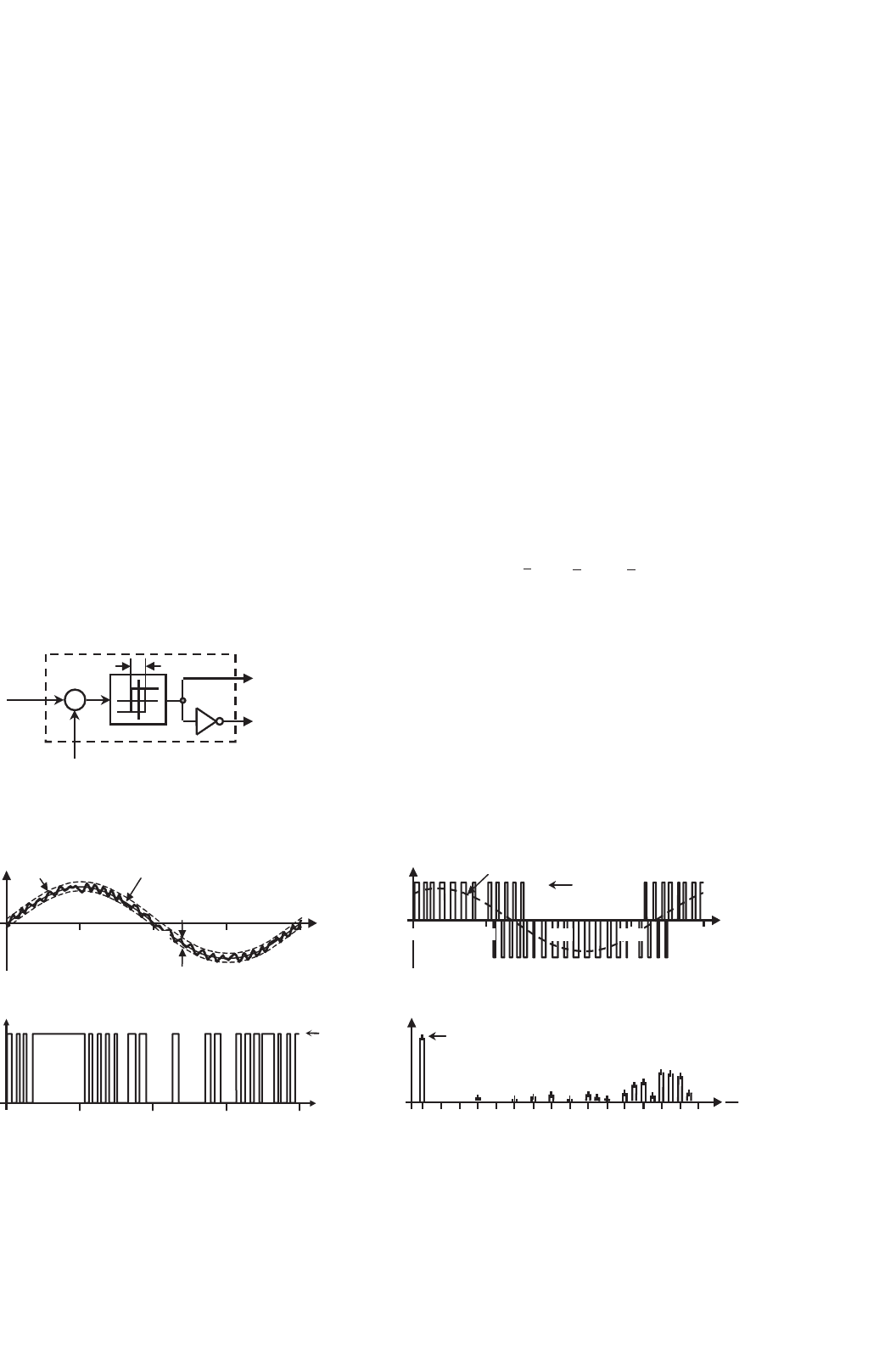
A. Hysteresis Current Control
The main purpose here is to force the ac line current to follow
a given reference. The status of the power valves S
1
and S
4
are changed whenever the actual i
oa
current goes beyond a
given reference i
oa,ref
±i/2. Figure 15.41 shows the hysteresis
current controller for phase a. Identical controllers are used in
phase b and c. The implementation of this controller is simple
as it requires an operational amplifier (op-amp) operating in
the hysteresis mode, thus the controller and modulator are
combined in one unit.
Unfortunately, there are several drawbacks associated with
the technique itself. First, the switching frequency cannot be
predicted as in carrier-based modulators and therefore the har-
monic content of the ac line voltages and currents becomes
random (Fig. 15.42d). This could be a disadvantage when
designing the filtering components. Second, as three-phase
loads do not have the neutral connected as in ASDs, the load
currents add up to zero. This means that only two ac line
currents can be controlled independently at any given instant.
Therefore, one of the hysteresis controllers is redundant at a
S
1
+
i
oa,ref
i
oa
−
S
4
phase a
∆i
FIGURE 15.41 The three-phase VSI. Hysteresis current control
(phase a).
180180 360360
m
27090
ωt
i
oa
i
oa,ref
∆i
360
ωt
v
ab
v
ab1
v
i
(a) (c)
180 270 90 360
ωt
0
S
1
on
157931923312711511317212925
v
ab
f
f
o
0.8·0.866·v
i
(b) (d)
180 360
0 180 27090
FIGURE 15.42 The three-phase VSI. Ideal waveforms for hysteresis current control: (a) actual ac load current and reference; (b) switch S
1
state; (c)
ac output voltage; and (d) ac output voltage spectrum.
given time. This explains why the load current goes beyond
the limits and introduces limit cycles (Fig. 15.42a). Finally,
although the ac load currents add up to zero, the controllers
cannot ensure that all load line currents feature a zero dc
component in one load cycle.
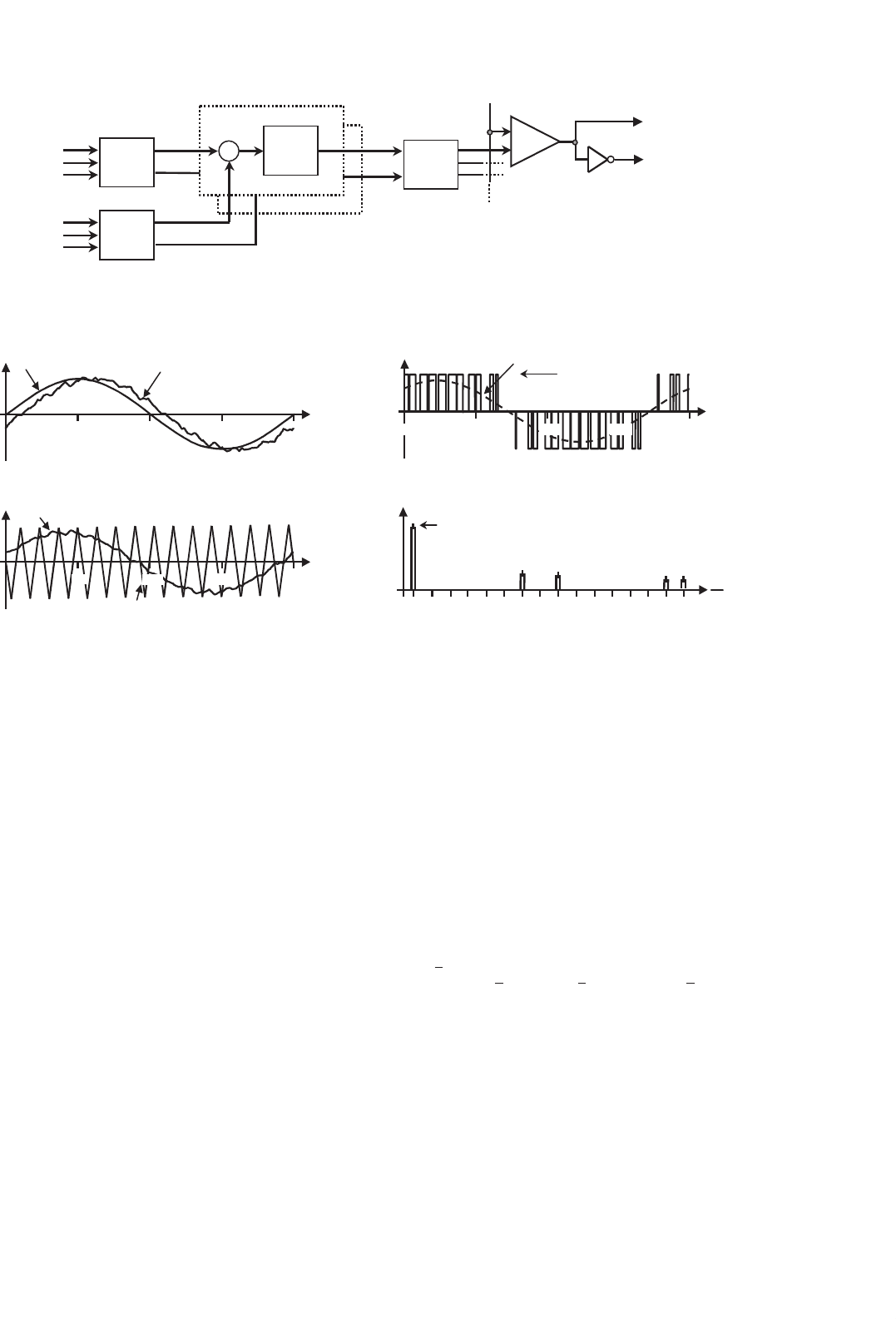
B. Linear Control of VSIs
Proportional and proportional-integrative controllers can also
be used in VSIs. The main purpose is to generate the modulat-
ing signals v
ca
, v
cb
, and v
cc
in a closed-loop fashion as depicted
in Fig. 15.43. The modulating signals can be used by a carrier-
based technique such as the SPWM (as depicted in Fig. 15.43)
or by space vector modulation. Because the load line currents
add up to zero, the load line current references must add up to
zero. Thus, the abc/αβγ transformation can be used to reduce
to two controllers the overall implementation scheme as the
γ component is always zero. This avoids limit cycles in the ac
load currents.
The transformation of a set of variables in the stationary abc
frame x
abc
into a set of variables in the stationary αβ frame x
ab
is given by
x
ab
=
2
3
1 −1/2 −1/2
0
√
3/2 −
√
3/2
x
abc
(15.73)
The selection of the controller (P, PI,...) is done according
to the control procedures such as steady-state error, settling
time, overshoot, and so forth. Figure 15.44 shows the rele-
vant waveforms of a VSI SPWM controlled by means of a
PI controller as shown in Fig. 15.43.
Although it is difficult to prove that no limit cycles are
generated, the ac line current appears very much sinusoidal.
Moreover, the ac line voltage generated by the VSI preserves
the characteristics of such waveforms generated by SPWM
modulators. This is confirmed by the harmonic spectrum
384 J. R. Espinoza
v
ca
S
1
+
i
oα,ref
i
oα
−
S
4
phase α
contr.
(P, PI,...)
abc/αβ
abc/αβ
v
cα
αβ/abc
v
cβ
v
∆
+
−
i
oβ,ref
i
o
β
i
oa,ref
phase β
i
oa
FIGURE 15.43 The three-phase VSI. Feedback control based on linear controllers.
180 27090
ωt
i
oa,ref
i
oa
90 360
ωt
v
ab
v
ab1
v
i
(a) (c)
360
ωt
v
ca
v
D
157931923312711511317212925
v
ab
f
f
o
0.8·0.866·v
i
(b)
(d)
360
180 27090
180 2700
FIGURE 15.44 The three-phase VSI. Ideal waveforms for a PI controller in a feedback loop (m
a
= 0.8, m
f
= 15): (a) actual ac load current and
reference; (b) carrier and modulating signals; (c) ac output voltage; and (d) ac output voltage spectrum.
shown in Fig. 15.44d, where the first set of characteris-
tic harmonics are around the normalized carrier frequency
m
f
= 15.
However, an error between the actual i
oa
and the ac line cur-
rent reference i
oa,ref
can be observed (Fig. 15.44a). This error
is inherent to linear controllers and cannot be totally elimi-
nated, but it can be minimized by increasing the gain of the
controller. However, the noise in the circuit is also increased,
which could deteriorate the overall performance of the control
scheme. The inherent presence of the error in this type of con-
trollers is due to the fact that the controller needs a sinusoidal
error to generate sinusoidal modulating signals v
ca
, v
cb
, and v
cc
,
as required by the modulator. Therefore, an error must exist
between the actual and the ac line current references.
Nevertheless, as current-controlled VSIs are actually the
inner loops in many control strategies, their inherent errors
are compensated by the outer loop. This is the case of ASDs,
where the outer speed loop compensates the inner current
loops. In general, if the outer loop is implemented with dc
quantities (such as speed), it can compensate the ac inner loops
(such as ac line currents). If it is mandatory that a zero steady-
state error be achieved with the ac quantities, then a stationary
(abc frame) to rotating (dq frame) transformation is a valid
alternative to use.
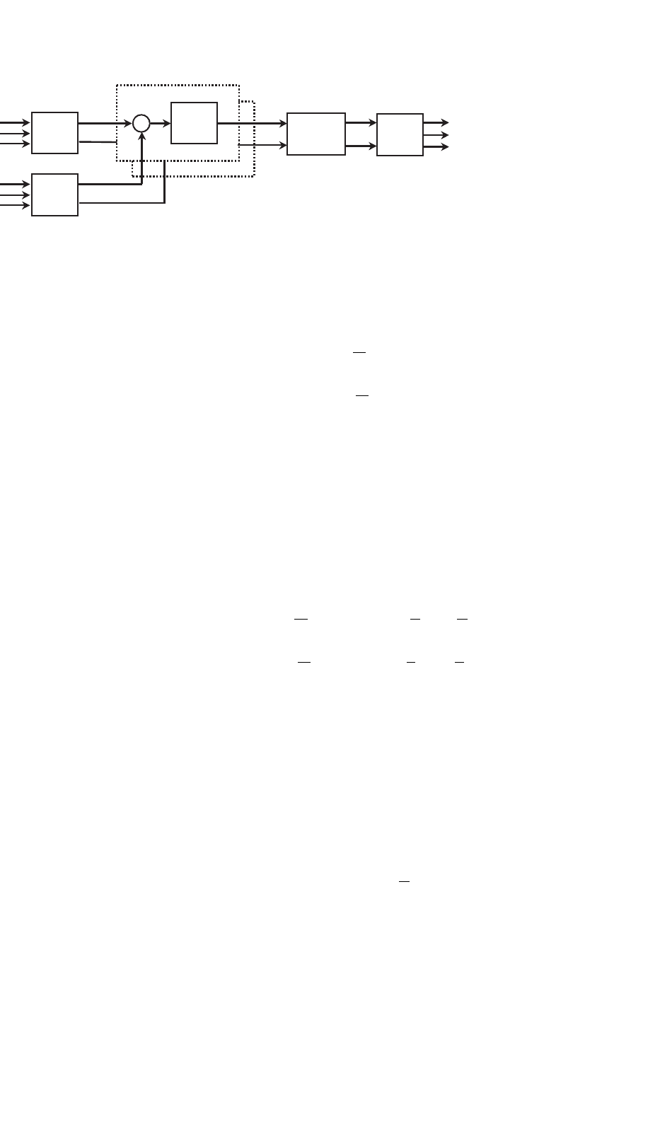
C. Linear Control of VSIs in a Rotating Frame
The rotating dq transformation allows ac three-phase circuits
to be operated as if they were dc circuits. This is based upon a
mathematical operation, that is the transformation of a set of
variables in the stationary abc frame x
abc
into a set of variables
in the rotating dq0 frame x
dq0
. The transformation is given by
x
dq
=
2
3
sin(ωt) sin(ωt − 2π/3) sin(ωt −4π/3)
cos(ωt ) cos(ωt −2π/3) cos(ωt −4π/3)
1/
√
21/
√
21/
√
2
x
abc
(15.74)
where ω is the angular frequency of the ac quantities. For
instance, the current vector given by
i
abc
=
i
a
i
b
i
c
=
Isin(ωt −ϕ)
Isin(ωt −2π/3 − ϕ)
Isin(ωt −4π/3 − ϕ)
(15.75)
15 Inverters 385
v
ca
+
i
od,ref
i
od
−
phase d
contr.
(PI,...)
abc/dq
abc/dq
m
d
dq/abc
m
q
i
oq,ref
i
oq
i
oa,ref
phase q
i
oa
decoupling
block
v
cd
v
cq
FIGURE 15.45 The three-phase VSI. Feedback control based on dq0 transformation.
becomes the vector
i
dq0
=
i
d
i
q
i
0
=
Icos(ϕ)
−Isin(ϕ)
0
(15.76)
where I and ϕ are the amplitude and phase of the line currents,
respectively. It can be observed that: (a) the zero component i
0
is always zero as the three-phase quantities add up to zero; and
(b) the d and q components i
d
, i
q
are dc quantities. Thus, linear
controllers should help to achieve zero steady-state error. The
control strategy shown in Fig. 15.45 is an alternative where the
zero-component controller has been eliminated due to fact
that the line currents at the load side add up to zero.
The controllers in Fig. 15.45 include an integrator that gen-
erates the appropriate dc outputs m
d
and m
q
even if the actual
and the line current references are identical. This ensures that
the zero steady-state error is achieved. The decoupling block
in Fig. 15.45 is used to eliminate the cross-coupling effect gen-
erated by the dq0 transformation and to allow an easier design
of the parameters of the controllers.
The dq0 transformation requires the intensive use of multi-
plications and trigonometric functions. These operations can
readily be done by means of digital microprocessors. Also,
analog implementations would indeed be involved.
15.5.4 Feedback Techniques in Current
Source Inverters
Duality indicates that CSIs should be controlled as equally as
VSIs except that the voltages become currents and the currents
become voltages. Thus, hystersis, linear and dq linear-based
control strategies are also applicable to CSIs; however, the con-
trolled variables are the load voltages instead of the load line
currents.
For instance, the linear control of a CSI based on a dq
transformation is depicted in Fig. 15.46. In this case, a passive
balanced load is considered. In order to show that zero steady-
state error is achieved, the per phase equations of the converter
are written as
C
d
dt
v
abc
p
= i
abc
o
−i
abc
l
(15.77)
L
d
dt
i
abc
l
= v
abc
p
−Ri
abc
l
(15.78)
the ac line currents are in fact imposed by the modulator and
they satisfy
i
abc
o
= i
i
i
abc
c
(15.79)
Replacing Eq. (15.79) into the model of the converter
Eqs. (15.77) and (15.78), using the dq0 transformation and
assuming null zero component, the model of the converter
becomes
d
dt
v
dq
p
=−Wv
dq
p
+
i
i
C
i
dq
c
−
1
C
i
dq
l
(15.80)
d
dt
i
dq
l
=−Wi
dq
l
+
1
L
v
dq
p
−
R
L
i
dq
l
(15.81)
where W is given by
W =
0 −ω
ω 0
(15.82)
A first approximation is to assume that the decoupling block
is not there; in other words, i
dq
c
= m
dq
. On the other hand, the
model of the controllers can be written as
m
dq
= k
v
dq
p,ref
−v
dq
p
+
1
T
t
−∞
v
dq
p,ref
−v
dq
p
dt (15.83)
where k and T are the proportional and integrative gains
of the PI controller that are chosen to achieve a desired
dynamic response. Combining the model of the controllers
and the model of the converter in dq coordinates and using
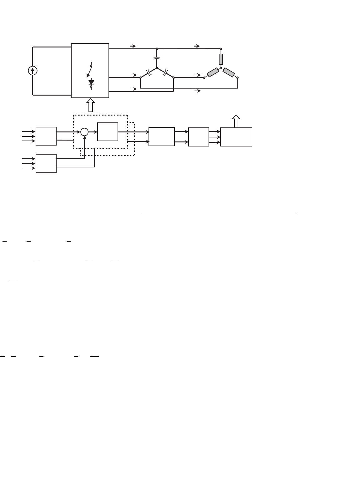
386 J. R. Espinoza
i
ca
+
v
pd,ref
v
nd
−
phase d
contr.
(PI,...)
abc/dq
abc/dq
m
d
dq/abc
m
q
v
pq,ref
v
nq
v
pa,ref
phase q
v
an
decoupling
block
i
cd
i
cq
i
oa
+
−
v
ab
i
ob
i
oc
+
−
v
bc
a
b
c
CSI
v
an
v
bn
v
cn
+
−
+
+
n
i
i
+
−
v
i
i
la
i
lc
i
lb
space-vector
modulator
S
1-6
S
1-6
a
−
+
n
b
c
R,L
C
FIGURE 15.46 The three-phase CSI. Feedback control based on dq0 transformation.
the Laplace transform, the following relationship between the
reference and actual load-phase voltages is found:
v
dq
p
=
i
i
C
sk +
1
T
sI +W +
R
L
I
×
sI +W +
R
L
I
s
2
I +s
W +
i
i
C
kI
+
i
i
CT
I
+
s
LC
I
−1
v
dq
p,ref
(15.84)
Finally, in order to prove that the zero steady-state error
is achieved for step inputs in either the d or q component
of the load-phase voltage reference, the previous expression is
evaluated in s = 0. This results in the following:
v
dq
p
=
i
i
C
1
T
W +
R
L
I
W +
R
L
I
i
i
CT
I
−1
v
dq
p,ref
= v
dq
p,ref
(15.85)
As expected, the actual and reference values are identical.
Finally, the relationship in Eq. (15.84) is a matrix that is not
diagonal. This means that both the actual and the reference
load-phase voltages are coupled. In order to obtain a decou-
pled control, the decoupling block in Fig. 15.46 should be
properly chosen.
15.6 Regeneration in Inverters
Industrial applications are usually characterized by a power
flow that goes from the ac distribution system to the load. This
is, for example, the case of an ASD operating in the motoring
mode. In this instance, the active power flows from the dc side
to the ac side of the inverter. However, there are an important
number of applications in which the load may supply power
to the system. Moreover, this could be an occasional condi-
tion as well as a normal operating condition. This is known as
the regenerative operating mode. For example, when an ASD
reduces the speed of an electrical machine this can be consid-
ered a transient condition. Downhill belt conveyors in mining
applications can be considered as a normal operating condi-
tion. In order to simplify the notation, it could be said that an
inverter operates in the motoring mode when the power flows
from the dc to the ac side, and in the regenerative mode when
the power flows from the ac to the dc side.
15.6.1 Motoring Operating Mode in
Three-phase VSIs
This is the case where the power flows from the dc side to
the ac side of the inverter. Figure 15.47 shows a simplified
scheme of an ASD where the motor has been modeled by
three RLe branches, where the sources e
abc
are the back-emf.
Because the ac line voltages applied by the inverter are imposed
by the pulsewidth modulation technique being used, they can
be adjusted according to specific requirements. In particular,
Fig. 15.48 shows the relevant waveforms in steady state for the
15 Inverters 387
v
as
i
oa
+
−
v
ab
N
i
i
+
−
v
i
/2
+
−
C
+
C
−
i
ob
i
oc
+
−
v
bc
a
b
c
VSI
v
an
v
bn
v
cn
n
Diode
Rectifier
i
sa
v
bs
v
cs
R
L
e
a
e
b
e
c
v
i
/2
FIGURE 15.47 Three-phase VSI topology with a diode-based front-end rectifier.
360 540180 720
ωt
0
v
i
V
i
ωt
v
an
v
an1
0.667 v
i
360 540180 720
(a)
(d)
ωt
i
i
I
i
360 540180
720
ωt
e
a
i
la
360 540180 720
(b) (e)
ωt
v
ab
v
ab1
v
i
360 540180 720
ωt
p
l
360 540180 720
(c) (f)
0
0
0
0
0
FIGURE 15.48 The ASD based on a VSI. Motoring mode: (a) dc bus voltage; (b) dc bus current; (c) ac line-load voltage; (d) ac phase-load voltage;
(e) motor line current and back-emf; and (f) shaft power.
motoring operating mode of the ASD. To simplify the analysis,
a constant dc bus voltage v
i
= V
i
has been considered.
It can be observed that: (i) the dc bus current i
i
features
a dc value I
i
that is positive; and (ii) the motor line current
is in phase with the back-emf. Both features confirm that the
active power flows from the dc source to the motor. This is
also confirmed by the shaft power plot (Fig. 15.48f), which is
obtained as:
p
l
(t) = e
a
(t)i
la
(t) + e
b
(t)i
lb
(t) + e
c
(t)i
lc
(t) (15.86)
15.6.2 Regenerative Operating Mode in
Three-phase VSIs
The back-emf sources e
abc
are functions of the machine speed
and as such they ideally change just as the speed changes.
The regeneration operating mode can be achieved by prop-
erly modifying the ac line voltages applied to the machine.
This is done by the speed outer loop that could be based
on a scalar (e.g. V /f ) or vectorial (e.g. field-oriented) control
strategy. As indicated earlier, there are two cases of regenerative
operating modes.
A. Occasional Regenerative Operating Mode
This mode is required during transient conditions such as in
occasional braking of electrical machines (ASDs). Specifically,
the speed needs to be reduced and the kinetic energy is taken
into the dc bus. Because the motor line voltage is imposed by
the VSI, the speed reduction should be done in such a way that
the motor line currents do not exceed the maximum values.
This boundary condition will limit the ramp-down speed to a
minimum, but shorter braking times will require a mechanical
braking system.