Power electronic handbook
Подождите немного. Документ загружается.

358 J. R. Espinoza
and to perform fundamental magnitude control (N = 3), the
equations to be solved are the following:
cos(1α
1
) −cos(1α
2
) +cos(1α
3
) = (2 + π ˆv
o1
/v
i
)/4
cos(3α
1
) −cos(3α
2
) +cos(3α
3
) = 1/2
cos(5α
1
) −cos(5α
2
) +cos(5α
3
) = 1/2
(15.8)
where the angles α
1
, α
2
and α
3
are defined as shown
in Fig. 15.6a. The angles are found by means of iterative
algorithms as no analytical solutions can be derived. The angles
α
1
, α
2
, and α
3
are plotted for different values of ˆv
o1
/v
i
in
Fig. 15.7a. The general expressions to eliminate an even N −1
270 90 360
ωt
0
v
o
v
o1
−v
i
/2
α
1
α
3
α
2
360
ωt
0
v
o
v
o1
−v
i
/2
α
1
α
3
α
2
α
4
(a) (c)
1573 19 23 31271151 9 13 17 21 2925
v
o
f
f
o
0. 8
v
i
2
1573 19 23 31271151 9 13 17 21 2925
v
o
f
f
o
0. 8
v
i
2
(b) (d)
180 180 180 180 270 270 90 90 180 180 270 90
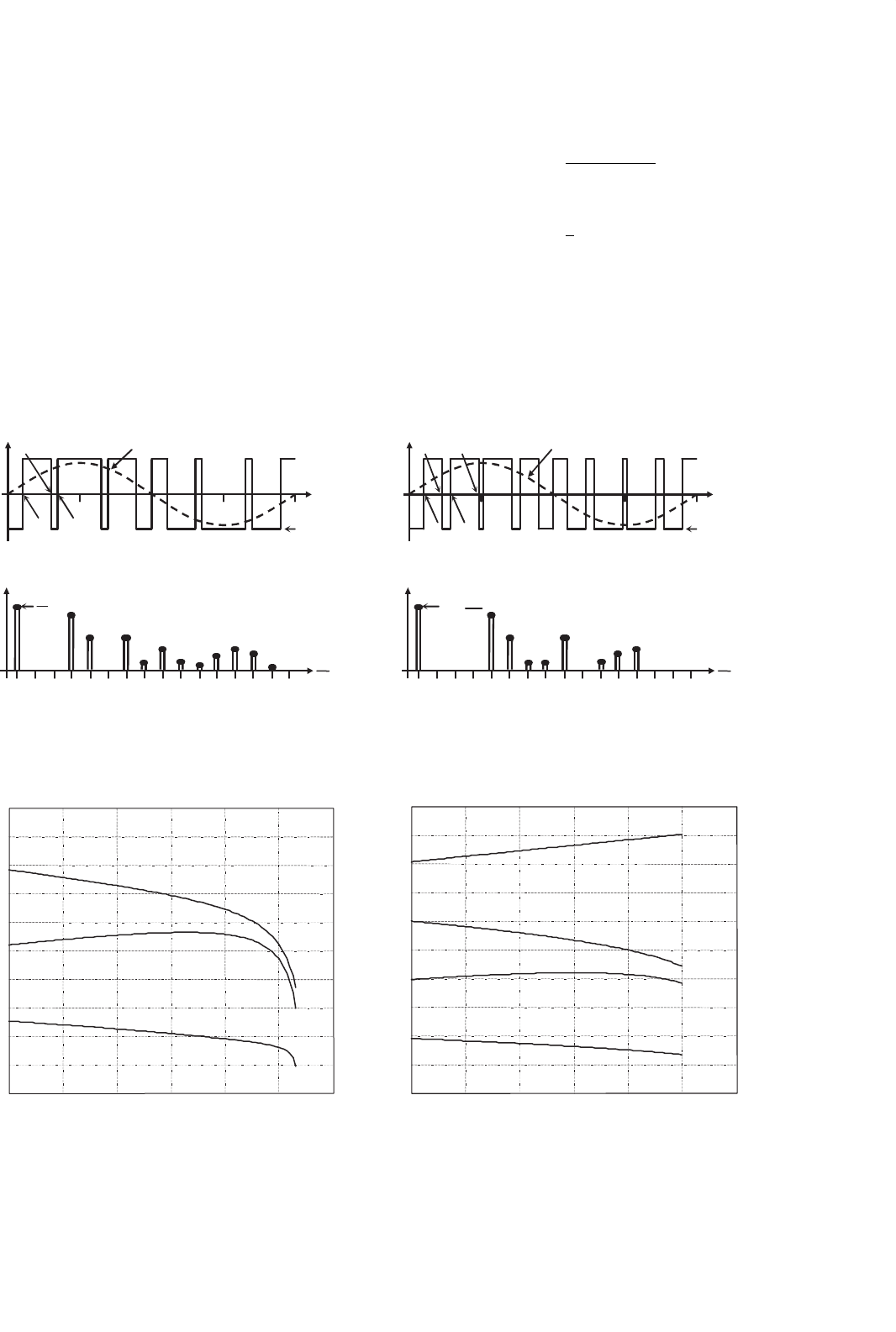
FIGURE 15.6 The half-bridge VSI. Ideal waveforms for the SHE technique: (a) ac output voltage for third and fifth harmonic elimination;
(b) spectrum of (a); (c) ac output voltage for third, fifth, and seventh harmonic elimination; and (d) spectrum of (c).
v
o1
/v
i
ˆ v
o1
/v
i
ˆ
0 0.1 0.2 0.3 0.4 0.5
0°
10°
20°
30°
40°
50°
60°
70°
80°
90°
100°
α
1
α
3
α
2
0 0.1 0.2 0.3 0.4 0.5
α
1
α
3
α
2
α
4
0°
10°
20°
30°
40°
50°
60°
70°
80°
90°
100°
(a) (b)
FIGURE 15.7 Chopping angles for SHE and fundamental voltage control in half-bridge VSIs: (a) third and fifth harmonic elimination and (b) third,
fifth, and seventh harmonic elimination.
(N −1 = 2, 4, 6, ...) number of harmonics are
−
N
k=1
(−1)
k
cos(α
k
) =
(2 +π ˆv
o1
)/v
i
4
−
N
k=1
(−1)
k
cos(nα
k
) =
1
2
for n = 3, 5, ...,2N − 1
(15.9)
where α
1
, α
2
,…, α
N
should satisfy α
1
<α
2
<···<α
N
<π/2.
Similarly, to eliminate an odd number of harmonics, for
instance the third, fifth, and seventh, and to perform the
15 Inverters 359
fundamental magnitude control (N − 1 = 3), the equations
to be solved are:
cos(1α
1
)−cos(1α
2
)+cos(1α
3
)−cos(1α
4
)=(2−π ˆv
o1
/v
i
)/4
cos(3α
1
)−cos(3α
2
)+cos(3α
3
)−cos(3α
4
)=1/2
cos(5α
1
)−cos(5α
2
)+cos(5α
3
)−cos(5α
4
)=1/2
cos(7α
1
)−cos(7α
2
)+cos(7α
3
)−cos(7α
4
)=1/2
(15.10)
where the angles α
1
, α
2
, α
3
, and α
4
are defined as shown in
Fig. 15.6b. The angles α
1
, α
2
, and α
3
are plotted for different
values of ˆv
o1
/v
i
in Fig. 15.7b. The general expressions to elimi-
nate an odd N −1(N −1 = 3, 5, 7, ...) number of harmonics
are given by
−
N
k=1
(−1)
k
cos(nα
k
) =
(2 −π ˆv
o1
)/v
i
4
−
N
k=1
(−1)
k
cos(nα
k
) =
1
2
for n = 3, 5, ...,2N −1
(15.11)
where α
1
, α
2
, ..., α
N
should satisfy α
1
<α
2
<···<α
N
<π/2.
To implement the SHE modulating technique, the modula-
tor should generate the gating pattern according to the angles
as shown in Fig. 15.7. This task is usually performed by digital
systems that normally store the angles in look-up tables.
D. DC Link Current
The split capacitors are considered a part of the inverter and
therefore an instantaneous power balance cannot be consid-
ered due to the storage energy components (C
+
and C
−
).
However, if a lossless inverter is assumed, the average power
absorbed in one period by the load must be equal to the
average power supplied by the dc source. Thus, we can write
T
0
v
i
(t) · i
i
(t) · dt =
T
0
v
o
(t) · i
o
(t) · dt (15.12)
where T is the period of the ac output voltage. For an inductive
load and a relatively high switching frequency, the load current
i
o
is nearly sinusoidal and therefore, only the fundamental
component of the ac output voltage provides power to the
load. On the other hand, if the dc link voltage remains constant
v
i
(t) = V
i
, Eq. (15.12) can be simplified to
T
0
i
i
(t)·dt =
1
V
i
T
0
√
2V
o1
sin(ωt)·
√
2I
o
sin(ωt −φ)·dt =I
i
(15.13)
where V
o1
is the fundamental rms ac output voltage, I
o
is the
rms load current, φ is an arbitrary inductive load power factor,
and I
i
is the dc link current that can be further simplified to
I
i
=
V
o1
V
i
I
o
cos(φ) (15.14)
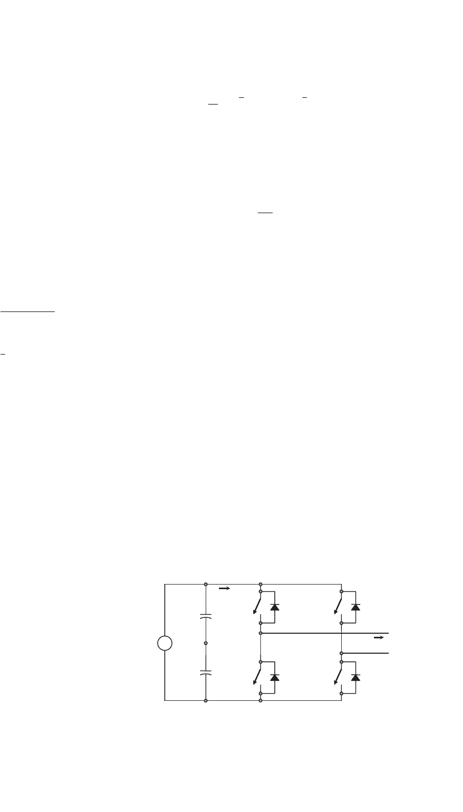
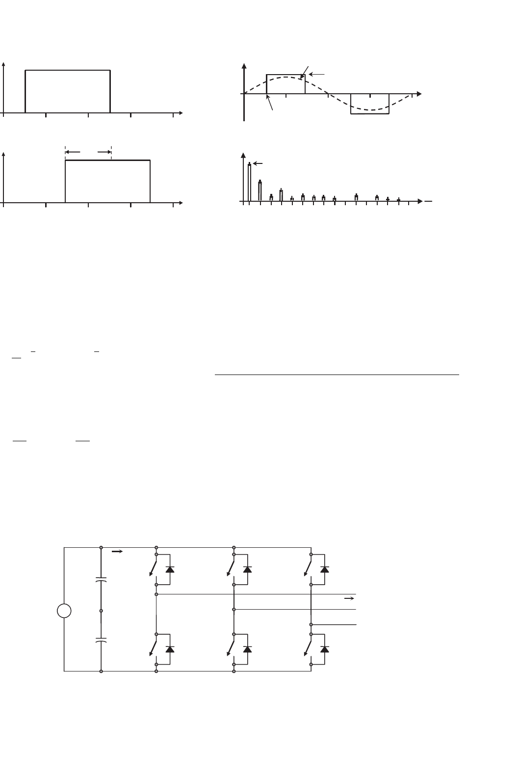
15.2.2 Full-bridge VSI
Figure 15.8 shows the power topology of a full-bridge VSI.
This inverter is similar to the half-bridge inverter; however,
a second leg provides the neutral point to the load. As expected,
both switches S
1+
and S
1−
(or S
2+
and S
2−
) cannot be
on simultaneously because a short circuit across the dc link
voltage source v
i
would be produced. There are four defined
(states 1, 2, 3, and 4) and one undefined (state 5) switch state
as shown in Table 15.2.
The undefined condition should be avoided so as to be
always capable of defining the ac output voltage always. In
order to avoid the short circuit across the dc bus and the unde-
fined ac output voltage condition, the modulating technique
should ensure that either the top or the bottom switch of each
leg is on at any instant. It can be observed that the ac output
voltage can take values up to the dc link value v
i
, which is
twice that obtained with half-bridge VSI topologies.
Several modulating techniques have been developed that
are applicable to full-bridge VSIs. Among them are the PWM
(bipolar and unipolar) techniques.
A. Bipolar PWM Technique
States 1 and 2 (Table 15.2) are used to generate the ac output
voltage in this approach. Thus, the ac output voltage waveform
features only two values, which are v
i
and −v
i
. To generate the
N
+
−
v
i
i
i
S
1+
a
S
1−
+
−
v
i
/2
+
−
v
i
/2
D
1+
D
1−
i
o
+
−
v
o
S
2+
b
S
2−
D
2+
D
2−
C
+
C
−
FIGURE 15.8 Single-phase full-bridge VSI.

360 J. R. Espinoza
TABLE 15.2 Switch states for a full-bridge single-phase VSI
State State # v
aN
v
bN
v
o
Components conducting
S
1+
and S
2−
are on and S
1−
and S
2+
are off 1 v
i
/2 −v
i
/2 v
i
S
1+
and S
2−
if i
o
> 0
D
1+
and D
2−
if i
o
< 0
S
1−
and S
2+
are on and S
1+
and S
2−
are off 2 −v
i
/2 v
i
/2 −v
i
D
1−
and D
2+
if i
o
> 0
S
1−
and S
2+
if i
o
< 0
S
1+
and S
2+
are on and S
1−
and S
2−
are off 3 v
i
/2 v
i
/2 0
S
1+
and D
2+
if i
o
> 0
D
1+
and S
2+
if i
o
< 0
S
1−
and S
2−
are on and S
1+
and S
2+
are off 4 −v
i
/2 −v
i
/2 0
D
1−
and S
2−
if i
o
> 0
S
1−
and D
2−
if i
o
< 0
S
1−
, S
2−
, S
1+
, and S
2+
are all off 5
−v
i
/2 v
i
/2 v
i
D
1−
and D
2+
if i
o
> 0
v
i
/2 −v
i
/2 −v
i
D
1+
and D
2−
if i
o
< 0
states, a carrier-based technique can be used as in half-bridge
configurations (Fig. 15.3), where only one sinusoidal modulat-
ing signal has been used. It should be noted that the on-state in
switch S
+
in the half-bridge corresponds to both switches S
1+
and S
2−
being in the on-state in the full-bridge configuration.
Similarly, S
−
in the on-state in the half-bridge corresponds
to both switches S
1−
and S
2+
being in the on-state in the
full-bridge configuration. This is called bipolar carrier-based
SPWM. The ac output voltage waveform in a full-bridge VSI
is basically a sinusoidal waveform that features a fundamental
component of amplitude ˆv
o1
that satisfies the expression
ˆv
o1
=ˆv
ab1
= v
i
m
a
(15.15)
in the linear region of the modulating technique (m
a
≤ 1),
which is twice that obtained in the half-bridge VSI. Identical
conclusions can be drawn for the frequencies and the ampli-
tudes of the harmonics in the ac output voltage and dc link
current, and for operations at smaller and larger values of
odd m
f
(including the overmodulation region (m
a
> 1)),
than in half-bridge VSIs, but considering that the maximum
ac output voltage is the dc link voltage v
i
. Thus, in the over-
modulation region the fundamental component of amplitude
ˆv
o1
satisfies the expression
v
i
< ˆv
o1
=ˆv
ab1
<
4
π
v
i
(15.16)
B. Unipolar PWM Technique
In contrast to the bipolar approach, the unipolar PWM tech-
nique uses the states 1, 2, 3, and 4 (Table 15.2) to generate the
ac output voltage. Thus, the ac output voltage waveform can
instantaneously take one of the three values, namely v
i
, −v
i
,
and 0. To generate the states, a carrier-based technique can be
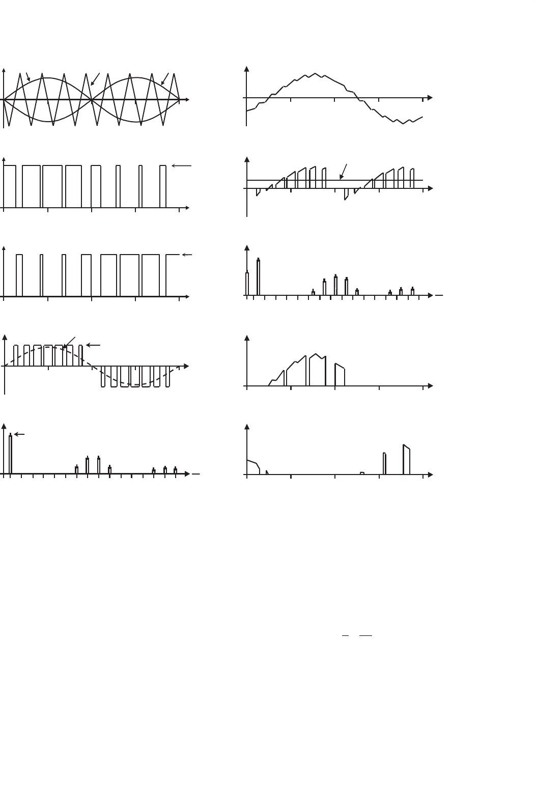
used as shown in Fig. 15.9, where two sinusoidal modulating
signals (v
c
and −v
c
) are used. The signal v
c
is used to generate
v
aN
, and −v
c
is used to generate v
bN
; thus v
bN 1
=−v
aN 1
.
On the other hand, v
o1
= v
aN 1
−v
bN 1
, = 2 ·v
aN 1
; thus ˆv
o1
=
2 ·ˆv
aN 1
= m
a
·v
i
This is called unipolar carrier-based SPWM.
Identical conclusions can be drawn for the amplitude of
the fundamental component and harmonics in the ac out-
put voltage and dc link current, and for operations at smaller
and larger values of m
f
(including the overmodulation region
(m
a
> 1)) than in full-bridge VSIs modulated by the bipolar
SPWM. However, because the phase voltages (v
aN
and v
bN
)
are identical but 180
◦
out of phase, the output voltage (v
o
=
v
ab
= v
aN
−v
bN
) will not contain even harmonics. Thus, if m
f
is taken even, the harmonics in the ac output voltage appear
at normalized odd frequencies f
h
centered around twice the
normalized carrier frequency m
f
and its multiples. Specifically,
h = lm
f
±kl= 2, 4, ... (15.17)
where k = 1, 3, 5, ...and the harmonics in the dc link current
appear at normalized frequencies f
p
centered around twice the
normalized carrier frequency m
f
and its multiples. Specifically,
p = lm
f
±k ± 1 l = 2, 4, ... (15.18)
where k = 1, 3, 5, ...This feature is considered to be an advan-
tage because it allows the use of smaller filtering components
to obtain high-quality voltage and current waveforms while
using the same switching frequency as in VSIs modulated by
the bipolar approach.
C. Selective Harmonic Elimination
In contrast to half-bridge VSIs, this approach is applied in
a per-line fashion for full-bridge VSIs. The ac output voltage
features odd half- and quarter-wave symmetry; therefore, even
harmonics are not present (ˆv
oh
= 0, h = 2, 4, 6, ...). More-
over, the ac output voltage waveform (v
o
= v
ab
in Fig. 15.8),
should feature N pulses per half-cycle in order to adjust the
fundamental component and eliminate N −1 harmonics. For
instance, to eliminate the third, fifth, and the seventh har-
monics and to perform fundamental component magnitude
15 Inverters 361
360
ωt
v
c
v
D
−v
c
18090 360
ωt
i
o
(a) (f)
180 27090 360
ωt
0
S
1+
on
180 27090 360
ωt
i
i
I
i
(b)
(g)
180 27090 360
ωt
0
S
2+
on
1579
f
f
o
3 19 23 312711511317212925
i
i
(c) (h)
18090 360
ωt
v
o
v
o1
v
i
180 27090 360
ωt
0
(d)
(i)
1573 19 23 3127119511317212925
v
o
f
f
o
0.8v
i
180 27090 360
ωt
0
i
D
1+
(e) (j)
i
S
1+
180180 2702709090
270270
180 27090
270
0
0
0
0
0
0
270
270270
FIGURE 15.9 The full-bridge VSI. Ideal waveforms for the unipolar SPWM (m
a
= 0.8, m
f
= 8): (a) carrier and modulating signals; (b) switch
S
1+
state; (c) switch S
2+
state; (d) ac output voltage; (e) ac output voltage spectrum; (f) ac output current; (g) dc current; (h) dc current spectrum;
(i) switch S
1+
current; and (j) diode D
1+
current.
control (N = 4), the equations to be solved are:
cos(1α
1
) −cos(1α
2
) +cos(1α
3
) −cos(1α
4
) = π ˆv
o1
/(v
i
4)
cos(3α
1
) −cos(3α
2
) +cos(3α
3
) −cos(3α
4
) = 0
cos(5α
1
) −cos(5α
2
) +cos(5α
3
) −cos(5α
4
) = 0
cos(7α
1
) −cos(7α
2
) +cos(7α
3
) −cos(7α
4
) = 0
(15.19)
where the angles α
1
, α
2
, α
3
, and α
4
are defined as shown
in Fig. 15.10a. The angles α
1
, α
2
, α
3
, and α
4
are plotted for
different values of ˆv
o1
/v
i
in Fig. 15.11a. The general expressions
to eliminate an arbitrary N − 1(N −1 = 3, 5, 7, ...) number
of harmonics are given by
−
N
k=1
(−1)
k
cos(nα
k
) =
π
4
ˆv
o1
v
i
−
N
k=1
(−1)
k
cos(nα
k
) = 0 for n = 3, 5, ...,2N −1
(15.20)
where α
1
, α
2
, ..., α
N
should satisfy α
1
<α
2
< ···<α
N
<π/2.
362 J. R. Espinoza
18090 360
ωt
v
o
v
o1
v
i
α
1
α
3
α
2
α
4
180 27090 360
ωt
v
o
v
o1
v
i
α
1
(a) (c)
15793 19 23 31271151 131721 2925
v
o
f
f
o
0.8v
i
15793 19 23 312711511317212925
v
o
f
f
o
0.8v
i
(b) (d)
2702702700 000
FIGURE 15.10 The half-bridge VSI. Ideal waveforms for the SHE technique: (a) ac output voltage for third, fifth, and seventh harmonic elimination;
(b) spectrum of (a); (c) ac output voltage for fundamental control; and (d) spectrum of (c).
v
o1
/v
i
ˆ v
o1
/v
i
ˆ
0 0.2 0.4 0.6 0.8 1.0 1.2
0°
10°
20°
30°
40°
50°
60°
70°
80°
90°
100°
α
1
α
3
α
2
α
4
α
1
0°
10°
20°
30°
40°
50°
60°
70°
80°
90°
100°
(a) (b)
0 0.2 0.4 0.6 0.8 1.0 1.2
FIGURE 15.11 Chopping angles for SHE and fundamental voltage control in half-bridge VSIs: (a) fundamental control and third, fifth, and seventh
harmonic elimination and (b) fundamental control.
Figure 15.10c shows a special case where only the fundamen-
tal ac output voltage is controlled. This is known as output
control by voltage cancellation, which derives from the fact
that its implementation is easily attainable by using two phase-
shifted square-wave switching signals as shown in Fig. 15.12.
The phase-shift angle becomes 2 · α
1
(Fig. 15.11b). Thus, the
amplitude of the fundamental component and harmonics in
the ac output voltage are given by
ˆv
oh
=
4
π
v
i
(−1)
(h−1)/2
h
cos (hα
1
) h = 1, 3, 5, ... (15.21)
It can also be observed in Fig. 15.12c that for α
1
= 0 square-
wave operation is achieved. In this case, the fundamental
ac output voltage is given by
ˆv
o1
=
4
π
v
i
(15.22)
where the fundamental load voltage can be controlled by the
manipulation of the dc link voltage.
D. DC Link Current
Due to the fact that the inverter is assumed lossless and
constructed without storage energy components, the instan-
taneous power balance indicates that,
v
i
(t) · i
i
(t) = v
o
(t) · i
o
(t) (15.23)
15 Inverters 363
S
1+
180 27090 360
ωt
0
180 27090 360
ωt
v
o
v
o1
v
i
α
1
(a) (c)
S
2+
2·α
1
180 27090 360
ωt
0
15793 19 23 31271151 131721 2925
v
o
f
f
o
0.8v
i
(b) (d)
00
FIGURE 15.12 The full-bridge VSI. Ideal waveforms for the output control by voltage cancellation: (a) switch S
1+
state; (b) switch S
2+
state;
(c) ac output voltage; and (d) ac output voltage spectrum.
For inductive load and relatively high switching frequencies,
the load current i
o
is nearly sinusoidal. As a first approxima-
tion, the ac output voltage can also be considered sinusoidal.
On the other hand, if the dc link voltage remains constant
v
i
(t) = V
i
, Eq. (15.23) can be simplified to
i
i
(t) =
1
V
i
√
2V
o1
sin(ωt) ·
√
2I
o
sin(ωt −φ) (15.24)
where V
o1
is the fundamental rms ac output voltage, I
o
is the
rms load current, and φ is an arbitrary inductive load power
factor. Thus, the dc link current can be further simplified to
i
i
(t) =
V
o1
V
i
I
o
cos(φ) −
V
o1
V
i
I
o
cos(2ωt −φ) (15.25)
The preceding expression reveals an important issue, that is,
the presence of a large second-order harmonic in the dc link
current (its amplitude is similar to the dc link current). This
second harmonic is injected back into the dc voltage source,
thus its design should consider it in order to guarantee a nearly
+
−
v
i
S
1
a
S
4
D
1
D
4
S
3
b
S
6
D
3
D
6
i
oa
+
−
v
ab
S
5
c
S
2
D
5
D
2
N
i
i
+
−
v
i
/2
+
−
v
i
/2
C
+
C
−
FIGURE 15.13 Three-phase VSI topology.
constant dc link voltage. In practical terms, the dc voltage
source is required to feature large amounts of capacitance,
which is costly and demands space, both undesired features,
especially in medium- to high-power supplies.
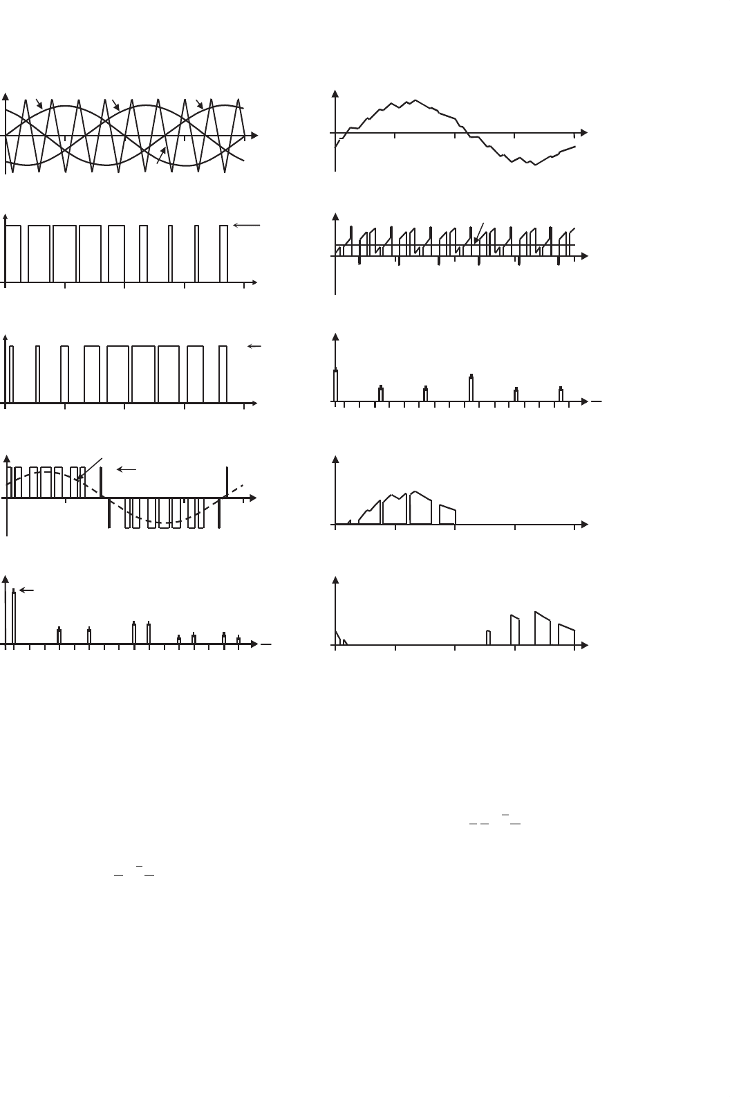
15.3 Three-phase Voltage Source
Inverters
Single-phase VSIs cover low-range power applications and
three-phase VSIs cover medium- to high-power applications.
The main purpose of these topologies is to provide a three-
phase voltage source, where the amplitude, phase, and fre-
quency of the voltages should always be controllable. Although
most of the applications require sinusoidal voltage waveforms
(e.g. ASDs, UPSs, FACTS, var compensators), arbitrary volt-
ages are also required in some emerging applications (e.g.
active filters, voltage compensators).
The standard three-phase VSI topology is shown in
Fig. 15.13 and the eight valid switch states are given
in Table 15.3. As in single-phase VSIs, the switches of any leg

364 J. R. Espinoza
TABLE 15.3 Valid switch states for a three-phase VSI
State State # v
ab
v
bc
v
ca
Space vector
S
1
, S
2
, and S
6
are on and
S
4
, S
5
, and S
3
are off
1 v
i
0 −v
i
v
1
= 1 + j0.577
S
2
, S
3
, and S
1
are on and
S
5
, S
6
, and S
4
are off
20v
i
−v
i
v
2
= j1.155
S
3
, S
4
, and S
2
are on and
S
6
, S
1
, and S
5
are off
3 −v
i
v
i
0 v
3
=−1 + j0.577
S
4
, S
5
, and S
3
are on and
S
1
, S
2
, and S
6
are off
4 −v
i
0 v
i
v
4
=−1 − j0.577
S
5
, S
6
, and S
4
are on and
S
2
, S
3
, and S
1
are off
50−v
i
v
i
v
5
=−j1.155
S
6
, S
1
, and S
5
are on and
S
3
, S
4
, and S
2
are off
6 v
i
−v
i
0 v
6
= 1 − j0.577
S
1
, S
3
, and S
5
are on and
S
4
, S
6
, and S
2
are off
7 000v
7
= 0
S
4
, S
6
, and S
2
are on and
S
1
, S
3
, and S
5
are off
8 000v
8
= 0
of the inverter (S
1
and S
4
, S
3
and S
6
,orS
5
and S
2
) cannot be
switched on simultaneously because this would result in a short
circuit across the dc link voltage supply. Similarly, in order to
avoid undefined states in the VSI, and thus undefined ac out-
put line voltages, the switches of any leg of the inverter cannot
be switched off simultaneously as this will result in voltages
that will depend upon the respective line current polarity.
Of the eight valid states, two of them (7 and 8 in Table 15.3)
produce zero ac line voltages. In this case, the ac line currents
freewheel through either the upper or lower components. The
remaining states (1 to 6 in Table 15.3) produce non-zero ac
output voltages. In order to generate a given voltage waveform,
the inverter moves from one state to another. Thus the result-
ing ac output line voltages consist of discrete values of voltages
that are v
i
,0,and−v
i
for the topology shown in Fig. 15.13.
The selection of the states in order to generate the given wave-
form is done by the modulating technique that should ensure
the use of only the valid states.
15.3.1 Sinusoidal PWM
This is an extension of the one introduced for single-phase
VSIs. In this case and in order to produce 120
◦
out-of-phase
load voltages, three modulating signals that are 120
◦
out-
of-phase are used. Figure 15.14 shows the ideal waveforms
of three-phase VSI SPWM. In order to use a single carrier
signal and preserve the features of the PWM technique, the
normalized carrier frequency m
f
should be an odd multiple
of 3. Thus, all phase voltages (v
aN
, v
bN
, and v
cN
) are identi-
cal, but 120
◦
out-of-phase without even harmonics; moreover,
harmonics at frequencies, a multiple of 3, are identical in
amplitude and phase in all phases. For instance, if the ninth
harmonic in phase aN is
v
aN 9
(t) =ˆv
9
sin(9ωt) (15.26)
the ninth harmonic in phase bN will be
v
bN 9
(t) =ˆv
9
sin
9(ωt −120
◦
)
=ˆv
9
sin(9ωt −1080
◦
) =ˆv
9
sin(9ωt) (15.27)
Thus, the ac output line voltage v
ab
= v
aN
− v
bN
will not
contain the ninth harmonic. Therefore, for odd multiple of 3
values of the normalized carrier frequency m
f
, the harmonics
in the ac output voltage appear at normalized frequencies f
h
centered around m
f
and its multiples, specifically, at
h = lm
f
±kl= 1, 2, ... (15.28)
where l = 1, 3, 5, ... for k = 2, 4, 6, ... and l = 2, 4, ... for
k = 1, 5, 7, ... such that h is not a multiple of 3. Therefore,
the harmonics will be at m
f
±2, m
f
±4, ...,2m
f
±1, 2m
f
±
5, ...,3m
f
±2, 3m
f
±4, ...,4m
f
±1, 4m
f
±5, .... For nearly
sinusoidal ac load current, the harmonics in the dc link current
are at frequencies given by
h = lm
f
±k ± 1 l = 1, 2, ... (15.29)
where l = 0, 2, 4, ... for k = 1, 5, 7, ... and l = 1, 3, 5, ...
for k = 2, 4, 6, ... such that h = l · m
f
± k is positive and
not a multiple of 3. For instance, Fig. 15.14h shows the sixth
harmonic (h = 6), which is due to h = 1 · 9 − 2 − 1 = 6.
The identical conclusions can be drawn for the operation
at small and large values of m
f
as for the single-phase con-
figurations. However, because the maximum amplitude of the
fundamental phase voltage in the linear region (m
a
≤ 1) is
v
i
/2, the maximum amplitude of the fundamental ac output
line voltage is
√
3v
i
/2. Therefore, one can write
ˆv
ab1
= m
a
√
3
v
i
2
0 < m
a
≤ 1 (15.30)
To further increase the amplitude of the load voltage, the
amplitude of the modulating signal ˆv
c
can be made higher
than the amplitude of the carrier signal ˆv
, which leads to
overmodulation. The relationship between the amplitude of
the fundamental ac output line voltage and the dc link volt-
age becomes non-linear as in single-phase VSIs. Thus, in the
overmodulation region, the line voltages range is
√
3
v
i
2
< ˆv
ab1
=ˆv
bc1
=ˆv
ca1
<
4
π
√
3
v
i
2
(15.31)
15.3.2 Square-wave Operation of
Three-phase VSIs
Large values of m
a
in the SPWM technique lead to full
overmodulation. This is known as square-wave operation as
illustrated in Fig. 15.15, where the power valves are on for 180
◦
.
15 Inverters 365
ωt
v
ca
v
D
v
cc
v
cb
180 27090
ωt
i
oa
(a) (f)
180 27090 360
ωt
0
S
1
on
18090 360
ωt
i
i
I
i
(b)
(g)
180 27090 360
ωt
0
S
3
on
1579
f
f
o
31923312711511317212925
i
i
(c) (h)
90 360
ωt
v
ab
v
o1
v
i
180 27090 360
ωt
0
i
S
1
i
D
1
(d)
(i)
157319233127115911317212925
v
ab
f
f
o
0.8·0.866·v
i
180 27090 360
ωt
0
(e)
(j)
180
180 2702709090 360360
180180 2702700
180 27090 360
180 2700
360
360360
270
2700 2700
00
FIGURE 15.14 The three-phase VSI. Ideal waveforms for the SPWM (m
a
= 0.8, m
f
= 9): (a) carrier and modulating signals; (b) switch S
1
state;
(c) switch S
3
state; (d) ac output voltage; (e) ac output voltage spectrum; (f) ac output current; (g) dc current; (h) dc current spectrum; (i) switch S
1
current; and (j) diode D
1
current.
In this operation mode, the VSI cannot control the load volt-
age except by means of the dc link voltage v
i
. This is based on
the fundamental ac line-voltage expression
ˆv
ab 1
=
4
π
√
3
v
i
2
(15.32)
The ac line output voltage contains the harmonics f
h
, where
h = 6 · k ± 1(k = 1, 2, 3, ...) and they feature amplitudes
that are inversely proportional to their harmonic order
(Fig. 15.15d). Their amplitudes are
ˆv
ab h
=
1
h
4
π
√
3
v
i
2
(15.33)
15.3.3 Sinusoidal PWM with Zero Sequence
Signal Injection
The restriction for m
a
(m
a
≤ 1) can be relaxed if a zero
sequence signal is added to the modulating signals before
they are compared to the carrier signal. Figure 15.16 shows
the block diagram of the technique. Clearly, the addition of
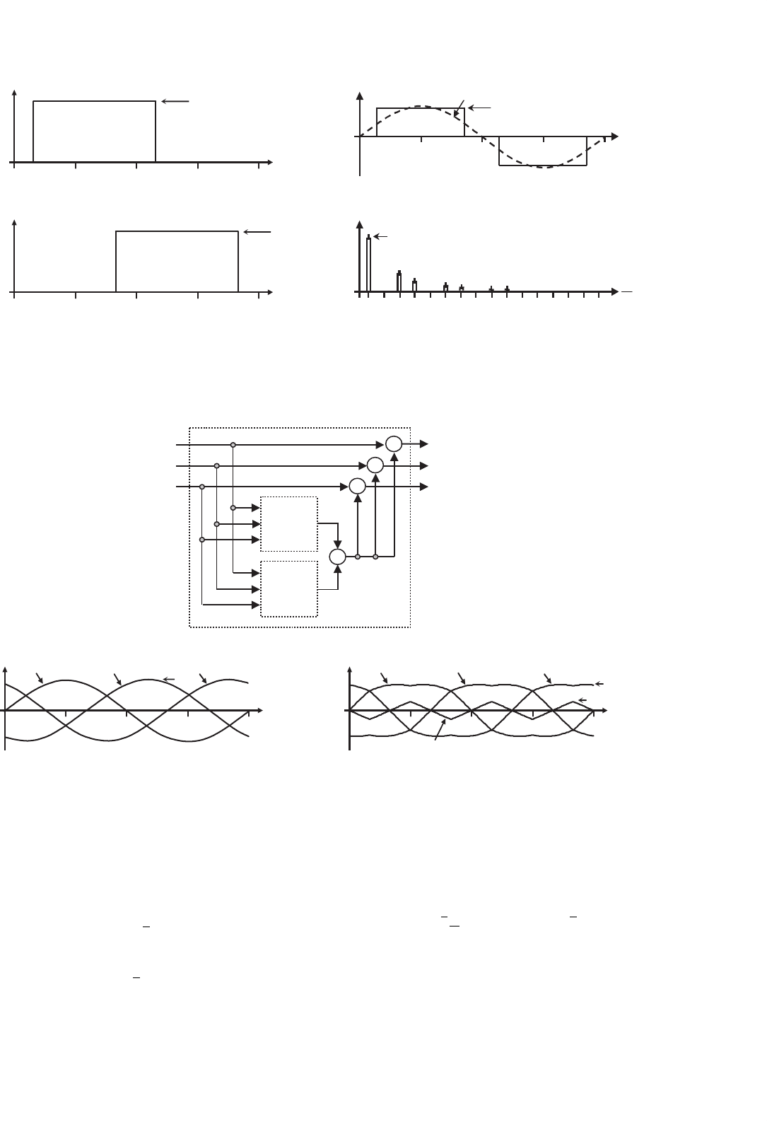
366 J. R. Espinoza
S
1
180 27090 360
ωt
0
on
27090
ωt
v
ab
v
ab1
v
i
(a)
(c)
S
3
180 27090 360
ωt
0
on
15793 19 23 312711511317212925
v
ab
f
f
o
1.1v
i
(b) (d)
180
180 3603600 180 3600
FIGURE 15.15 The three-phase VSI. Square-wave operation: (a) switch S
1
state; (b) switch S
3
state; (c) ac output voltage; and (d) ac output voltage
spectrum.
+
+
+
+
max{ }/3
min{ }/3
v
0
(a)
ωt
v
ca
u
ca
u
cb
u
cc
v
cc
v
cb
1.00
360
ωt
v
0
0.88
0.17
(b) (c)
u
cc
u
cb
u
ca
v
ca
v
cb
v
cc
180180 2702709090 180 27090180180 2702709090 360360180 27090 360
FIGURE 15.16 Zero sequence signal generator (m
a
= 1.0, m
f
= 9): (a) block diagram; (b) modulating signals; and (c) zero sequence and modulating
signals with zero sequence injection.
the zero sequence reduces the peak amplitude of the result-
ing modulating signals (u
ca
, u
cb
, u
cc
), while the fundamental
components remain unchanged. This approach expands the
range of the linear region as it allows the use of mod-
ulation indexes m
a
up to 2/
√
3 without getting into the
overmodulating region.
The maximum amplitude of the fundamental phase voltage
in the linear region
m
a
≤ 2/
√
3
is v
i
/2, thus, the maximum
amplitude of the fundamental ac output line voltage is v
i
.
Therefore, one can write
ˆv
ab1
= m
a
√
3
v
i
2
0 < m
a
≤ 2/
√
3
(15.34)
Figure 15.17 shows the ideal waveforms of a three-phase VSI
SPWM with zero injection for m
a
= 0.8.

15 Inverters 367
180 270 360
ωt
v
ca
v
cc
v
cb
180 27090
ωt
i
oa
(a) (f)
ωt
u
ca
u
cc
u
cb
vD
180 27090 360
ωt
i
i
I
i
(b) (g)
180 27090 360
ωt
0
S
1
on
1579
f
f
o
3 19 23 31271151 131721 2925
i
i
(c) (h)
90 360
ωt
v
ab
v
o1
v
i
180 27090 360
ωt
0
i
S
1
(d)
(i)
1573 19 23 31271151 9 13 17 21 2925
v
ab
f
f
o
0.8·0.866·v
i
180 27090 360
ωt
0
(e) (j)
i
D
1
9090
3603600
180
180 2702709090 360360
180180 2702700
90
3600
180 27090 360
180 2700
00
FIGURE 15.17 The three-phase VSI. Ideal waveforms for the SPWM (m
a
= 0.8, m
f
= 9) with zero sequence signal injection: (a) modulating signals;
(b) carrier and modulating signals with zero sequence signal injection; (c) switch S
1
state; (d) ac output voltage; (e) ac output voltage spectrum; (f) ac
output current; (g) dc current; (h) dc current spectrum; (i) switch S
1
current; and (j) diode D
1
current.
15.3.4 Selective Harmonic Elimination in
Three-phase VSIs
As in single-phase VSIs, the SHE technique can be applied
to three-phase VSIs. In this case, the power valves of each
leg of the inverter are switched so as to eliminate a given
number of harmonics and to control the fundamental phase-
voltage amplitude. Considering that in many applications, the
required line output voltages should be balanced and 120
◦
out
of phase, the harmonics multiples of 3 (h = 3, 9, 15, ...), which
could be present in the phase voltages (v
aN
, v
bN
, and v
cN
), will
not be present in the load voltages (v
ab
, v
bc
, and v
ca
). There-
fore, these harmonics are not required to be eliminated, thus
the chopping angles are used to eliminate only the harmonics
at frequencies h = 5, 7, 11, 13, ...as required.
The expressions to eliminate a given number of harmon-
ics are the same as those used in single-phase inverters. For
instance, to eliminate the fifth and seventh harmonics and per-
form fundamental magnitude control (N = 3), the equations