Power electronic handbook
Подождите немного. Документ загружается.

17 Multilevel Power Converters 459
I
cb
I
cc
I
ca
V
sb
I
Lc
I
La
I
Lb
V
La
series
inverter
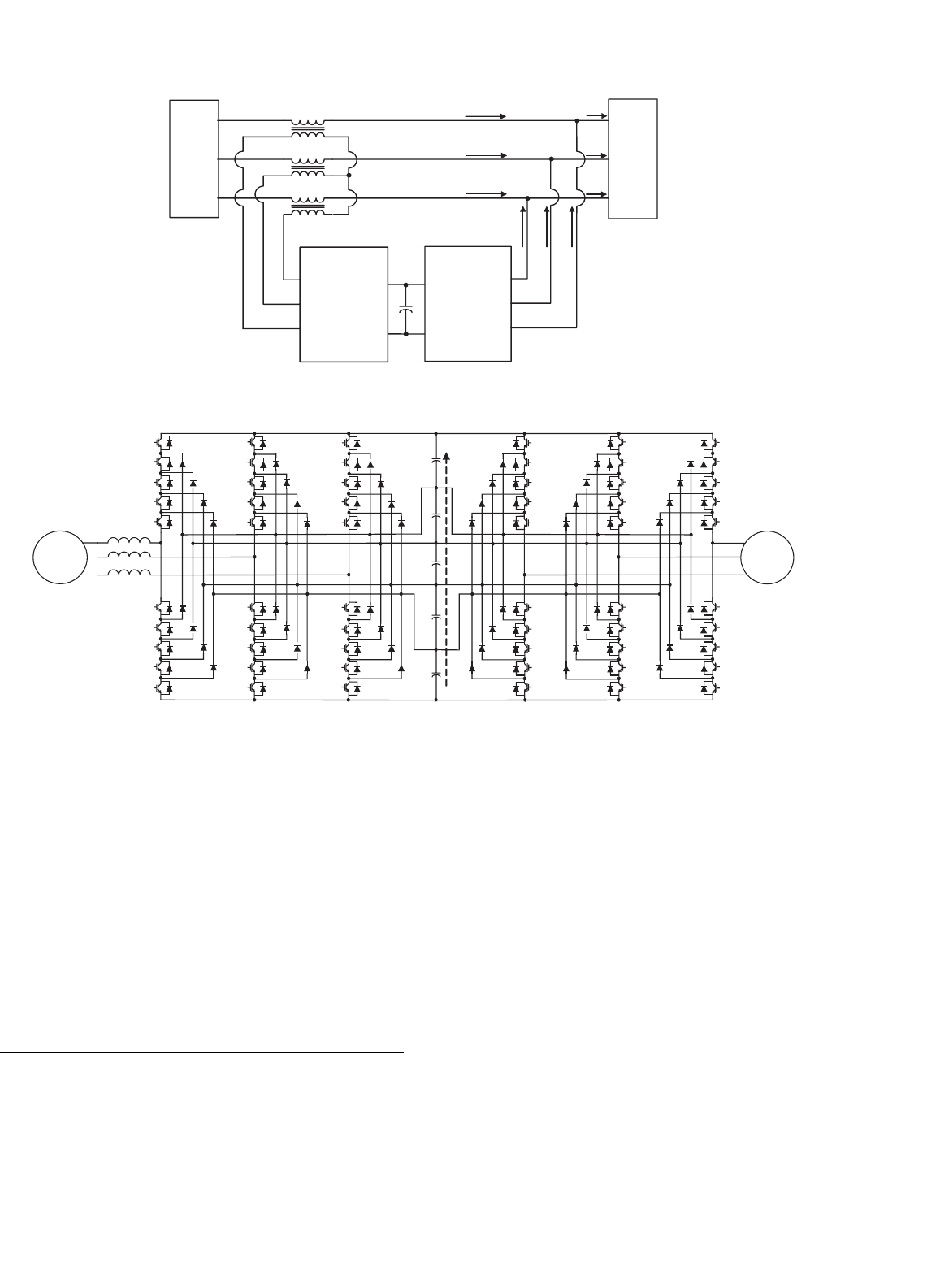
LoadUtility
I
sa
V
Lb
V
Lc
I
Sb
I
Sc
V
sa
V
sc
parallel
inverter
FIGURE 17.11 Series–parallel connection to electrical system of two back-to-back inverters.
VLa
VLc
VLb
Sa5
Sa4
Sa3
Sa2
D1
D2
D3
Sa1
D4
Sa'5
Sa'4
Sa'3
Sa'2
D4
D3
D2
Sa'1
D1
Sb5
Sb4
Sb3
Sb2
D1
D2
D3
Sb1
D4
Sb'5
Sb'4
Sb'3
Sb'2
D4
D3
D2
Sb'1
D1
Sc5
Sc4
Sc3
Sc2
D1
D2
D3
Sc1
D4
Sc'5
Sc'4
Sc'3
Sc'2
D
4
D3
D2
Sc'1
D1
5Vdc
Motor
Load
V4
V3
V2
V1
V0
C4
C3
C2
C1
V5
C5
VSa
VSc
VSb
Sa5
Sa4
Sa3
Sa2
D1
D2
D3
Sa1
D4
Sa'5
Sa'4
Sa'3
Sa'2
D4
D3
D2
Sa'1
D1
Sb5
Sb4
Sb3
Sb2
D1
D2
D3
Sb1
D4
Sb'5
Sb'4
Sb'3
Sb'2
D4
D3
D2
Sb'1
D1
Sc5
Sc4
Sc3
Sc2
D1
D2
D3
Sc1
D4
Sc'5
Sc'4
Sc'3
Sc'2
D4
D3
D2
Sc'1
D1
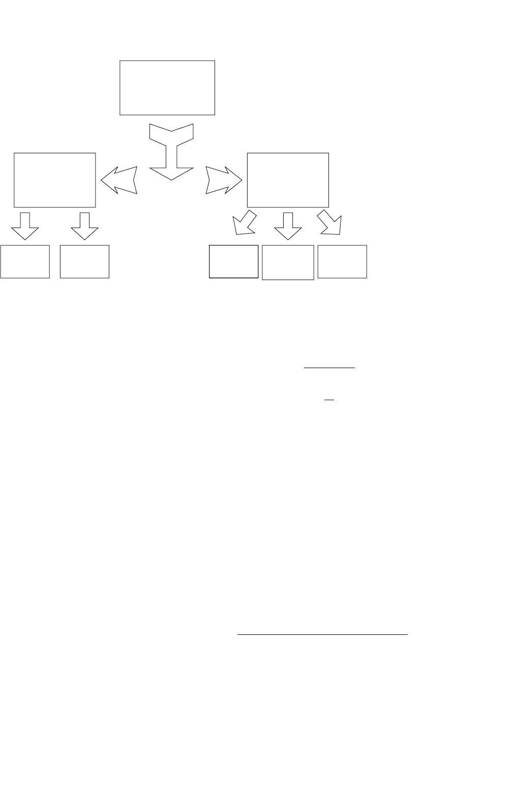
Gen
Source
ac-dc converter
dc-ac inverter
negative dc-rail
positive dc-rail
0
L
S
LS
LS
FIGURE 17.12 Six-level diode-clamped back-to-back converter structure.
Because a diode-clamped converter acting as a universal
power conditioner will be expected to compensate for harmon-
ics and/or operate in low amplitude modulation index regions,
a more sophisticated higher-frequency switch control than the
fundamental frequency switching method will be needed. For
this reason, multilevel space vector and carrier-based PWM
approaches are compared in the next section, as well as novel
carrier-based PWM methodologies.
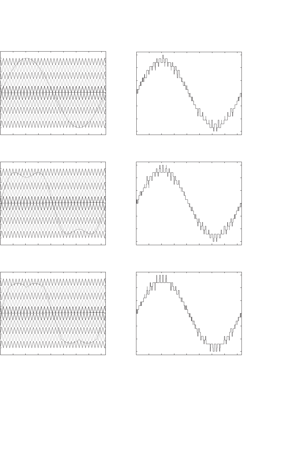
17.3 Multilevel Converter PWM
Modulation Strategies
Pulse width modulation strategies used in a conventional
inverter can be modified to use in multilevel converters. The
advent of the multilevel converter PWM modulation method-
ologies can be classified according to switching frequency as
illustrated in Fig. 17.13. The three multilevel PWM methods
most discussed in the literature have been multilevel carrier-
based PWM, selective harmonic elimination, and multilevel
space vector PWM, all are extensions of traditional two-level
PWM strategies to several levels. Other multilevel PWM meth-
ods have been used to a much lesser extent by researchers;
therefore, only the three major techniques will be discussed in
this chapter.
17.3.1 Multilevel Carrier-based PWM
Several different two-level, multilevel carrier-based PWM
techniques have been extended by previous authors as a means
for controlling the active devices in a multilevel converter. The
most popular and easiest technique to implement uses sev-
eral triangle carrier signals and one reference, or modulation,
signal per phase. Figure 17.14 illustrates three major carrier-
based techniques used in a conventional inverter that can be
460 S. Khomfoi and L. M. Tolbert
Multilevel converter
modulation strategies
Fundamental
Switching
Frequency
High Switching
Frequency PWM
Space
Vector
Control
Selective
Harmonic
Elimination
Space
Vector PWM
Sinusoidal
PWM
Selective
Harmonic
Elimination
PWM
FIGURE 17.13 Classification of PWM multilevel converter modulation strategies.
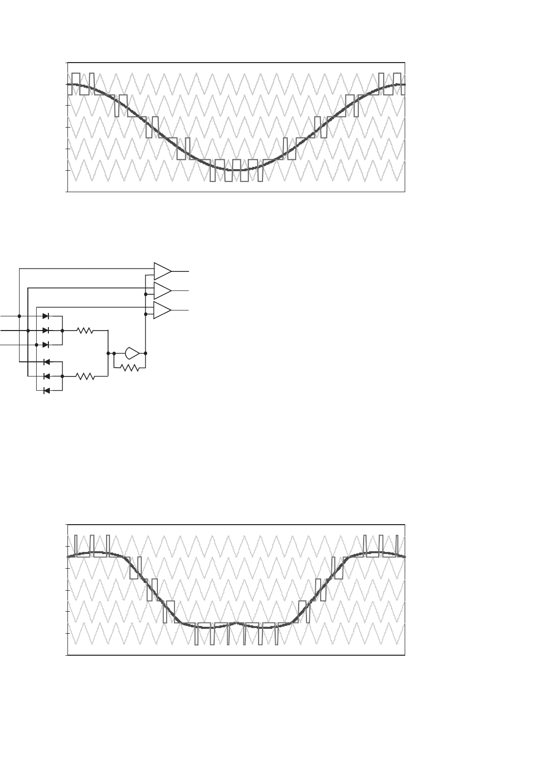
applied in a multilevel inverter: sinusoidal PWM (SPWM),
third harmonic injection PWM (THPWM), and space vector
PWM (SVM). SPWM is a very popular method in industrial
applications.
In order to achieve better dc link utilization at high modula-
tion indices, the sinusoidal reference signal can be injected by a
third harmonic with a magnitude equal to 25% of the funda-
mental, its line–line output voltage is shown in Fig. 17.14b.
As can be seen in Fig. 17.14b and c, the reference signals
have some margin at unity amplitude modulation index. Obvi-
ously, the dc utilization of THPWM and SVM are better than
SPWM in the linear modulation region. The dc utilization
means the ratio of the output fundamental voltage to the dc
link voltage. Other interesting carrier-based multilevel PWM
are subharmonic PWM (SH-PWM) and switching frequency
optimal PWM (SFO-PWM). In addition, some particular
aspects of these carrier-based methods are also discussed as
follows.
A. Subharmonic PWM
Carrara [48] extended SH-PWM to multiple levels as follows:
for an m-level inverter, m −1 carriers with the same frequency
f
c
and the same amplitude A
c
are disposed such that the bands
they occupy are contiguous. The reference waveform has peak-
to-peak amplitude A
m
, a frequency f
m
, and its zero centered
in the middle of the carrier set. The reference is continuously
compared with each of the carrier signals. If the reference is
greater than a carrier signal, then the active device correspond-
ing to that carrier is switched on, and if the reference is less
than a carrier signal, then the active device corresponding to
that carrier is switched off.
In multilevel inverters, the amplitude modulation index, m
a
,
and the frequency ratio, m
f
, are defined as
m
a
=
A
m
(m −1) ·A
c
(17.3)
m
f
=
f
c
f
m
(17.4)
Figure 17.15 shows a set of carriers (m
f
= 21) for a six-level
diode-clamped inverter and a sinusoidal reference, or modu-
lation waveform with an amplitude modulation index of 0.8.
The resulting output voltage of the inverter is also shown in
Fig. 17.15.
B. Switching Frequency Optimal PWM
Another carrier-based method that was extended to multi-
level applications by Menzies is termed SFO-PWM, and it is
similar to SH-PWM except that a zero sequence (triplen har-
monic) voltage is added to each of the carrier waveforms [49].
This method takes the instantaneous average of the maximum
and minimum of the three reference voltages
V
∗
a
, V
∗
b
, V
∗
c
and subtracts this value from each of the individual reference
voltages, i.e.
V
offset
=
max
V
∗
a
, V
∗
b
, V
∗
c
+min
V
∗
a
, V
∗
b
, V
∗
c
2
(17.5)
V
∗
aSFO
= V
∗
a
−V
offset
(17.6)
V
∗
bSFO
= V
∗
b
−V
offset
(17.7)
V
∗
cSFO
= V
∗
c
−V
offset
(17.8)
17 Multilevel Power Converters 461
0 0.002 0.004 0.006 0.008 0.01 0.012 0.014 0.016
−1
−0.8
−0.6
−0.4
−0.2
0
0.2
0.4
0.6
0.8
1
Time (sec.)
Modulation Signal
0 0.002 0.004 0.006 0.008 0.01 0.012 0.014 0.016
−600
−400
−200
0
200
400
600
Time (sec.)
Amplitude
0 0.002 0.004 0.006 0.008 0.01 0.012 0.014 0.016
−1
−0.8
−0.6
−0.4
−0.2
0
0.2
0.4
0.6
0.8
1
Time (sec.)
Modulation Signal
0 0.002 0.004 0.006 0.008 0.01 0.012 0.014 0.016
−600
−400
−200
0
200
400
600
Amplitude
Time (sec.)
0 0.002 0.004 0.006 0.008 0.01 0.012 0.014 0.016
−1
−0.8
−0.6
−0.4
−0.2
0
0.2
0.4
0.6
0.8
1
Time (sec.)
Modulation Signal
0 0.002 0.004 0.006 0.008 0.01 0.012 0.014 0.016
−600
−400
−200
0
200
400
600
Amplitude
Time (sec.)
(a)
(b)
(c)
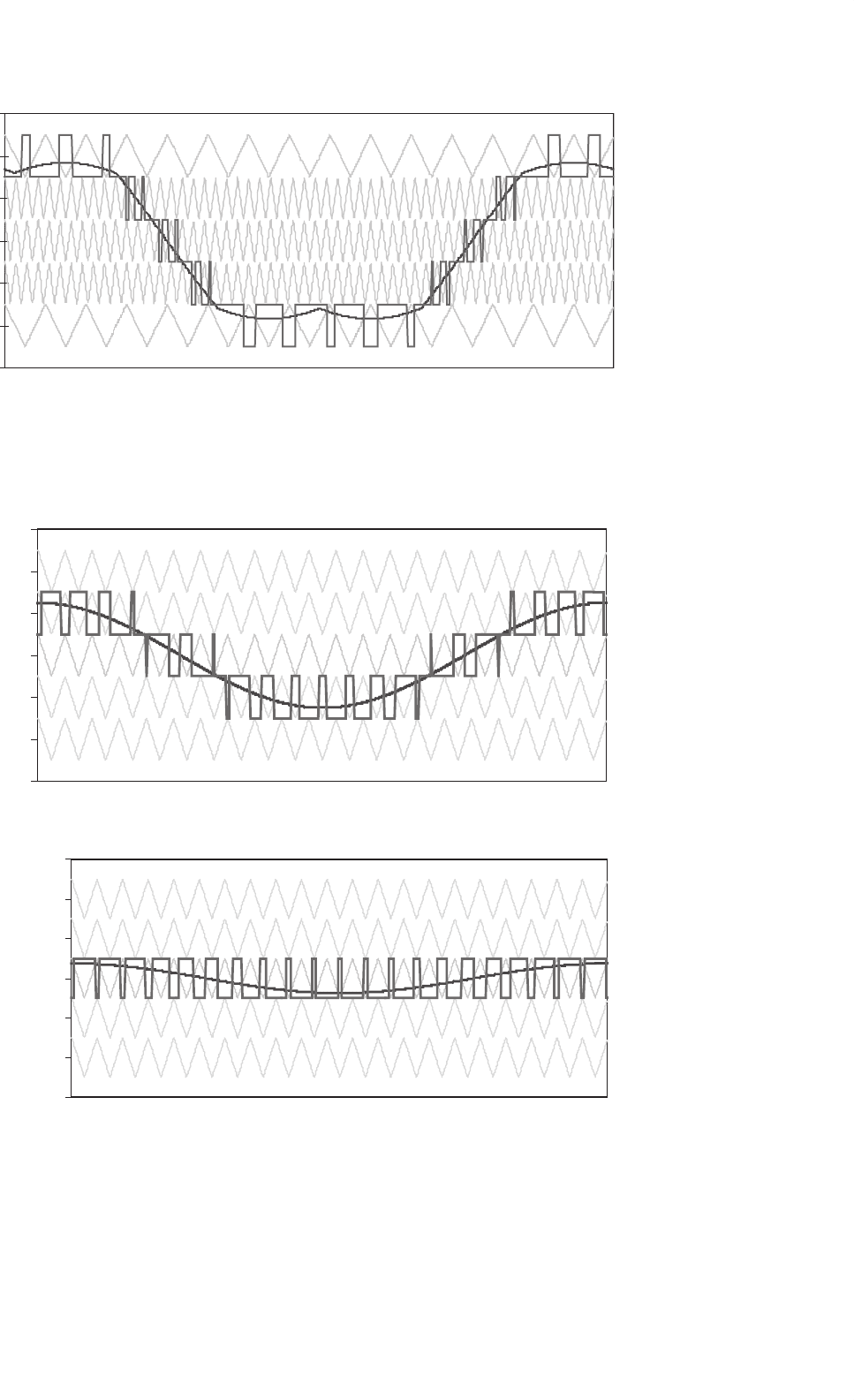
FIGURE 17.14 Simulation of modulation signals and their line–line output voltage using five separate dc sources (60 V each dc source) cascaded
multilevel inverter with three major conventional carrier-based PWM techniques at unity modulation index and 2 kHz switching frequency: (a) SPWM;
(b) THPWM; and (c) SVM.
462 S. Khomfoi and L. M. Tolbert
–3
–2
–1
0
1
2
3
time (sec.)
0.0167
0.0000 0.0833
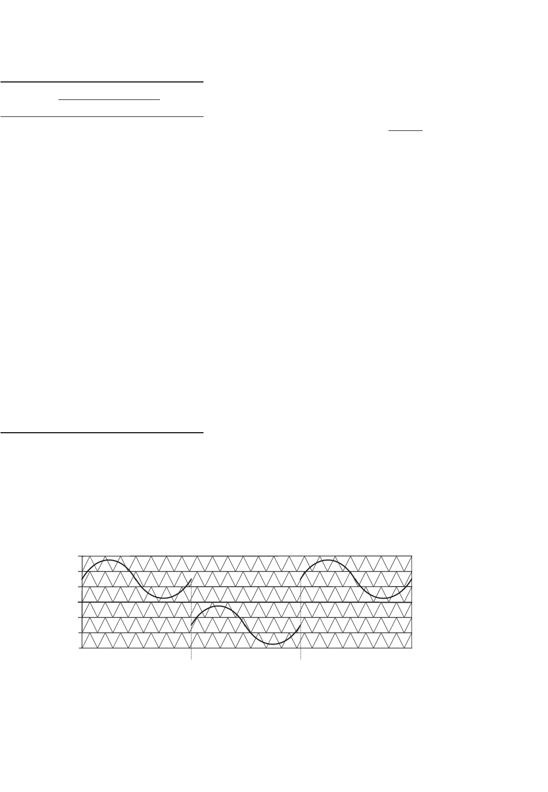
FIGURE 17.15 Multilevel carrier-based SH-PWM showing carrier bands, modulation waveform, and inverter output waveform (m = 6, m
f
= 21,
m
a
= 0.8).
Va
*
V
c
*
V
b
*
+
−
+
−
+
−
V
a
*
SFO
Vc
*
SFO
Vb
*
SFO
2R
2R
R
FIGURE 17.16 Analog circuit for zero sequence addition in SFO-PWM.
The addition of this triplen offset voltage centers all of the
three reference waveforms in the carrier band, which is equiva-
lent to using space vector PWM [50, 51]. The analog equivalent
of Eqs. (17.5–17.8) is shown in Fig. 17.16 [52]. The SFO-
PWM is illustrated in Fig. 17.17 for the same reference voltage
waveform that was used in Fig. 17.15. The resulting output
–3
–2
–1
0
1
2
3
time (sec.)
0.01670.0000 0.0833
FIGURE 17.17 Multilevel carrier-based SFO-PWM showing carrier bands, modulation waveform, and inverter output waveform (m = 6, m
f
= 21,
m
a
= 0.8).
voltage of the inverter is also shown in Fig. 17.17. The SFO-
PWM technique enables the modulation index to be increased
by 15% before the overmodulation region is reached.
For the SH-PWM and SFO-PWM techniques shown in
Figs. 17.15 and 17.17, the top and bottom switches are
switched much more often than the intermediate devices.
Methods to balance and/or reduce the device switchings
without an adverse effect on a multilevel inverter’s output volt-
age total harmonic distortion would be beneficial. Methods to
do just that are developed in [53]. A novel method to bal-
ance device switchings for all of the levels in a diode clamped
inverter has been demonstrated for SH-PWM and SFO-PWM
by varying the frequency for the different triangle wave carrier
bands as shown in Fig. 17.18 [53].
C. Modulation Index Effect on Level Utilization
For low amplitude modulation indices, a multilevel inverter
will not make use of all of its levels and at very low modula-
tion indices it operates as if it is a traditional two-level inverter.
Figure 17.19 shows two simulation results of what the output
voltage waveform looks like at amplitude modulation indices
17 Multilevel Power Converters 463
–3
–2
–1
0
1
2
3
time
(
sec.
)
0.0167
0.0000 0.0833
FIGURE 17.18 SFO-PWM where carriers have different frequencies (m
a
= 0.85, m
f
= 15 for Band
2
, Band
−2
; m
f
= 55 for Band
1
, Band
−1
;
Band
0
, ϕ = 0.10 rad).
−3
−2
−1
0
1
2
3
time (sec.)
Voltage (p.u.)
(a)
−3
−2
−1
0
1
2
3
time (sec.)
Voltage (p.u.)
(b)
FIGURE 17.19 Level reduction in a six-level inverter at low modulation indices: (a) SH-PWM, m = 6, m
a
= 0.5 and (b) SH-PWM, m = 6,
m
a
= 0.15.

464 S. Khomfoi and L. M. Tolbert
of 0.5 and 0.15. Figure 17.19a shows how the bottom and top
switches (S
a1
−S
a
1
,S
a5
−S
a
5
in Fig. 17.5) go unused for ampli-
tude modulation indices less than 0.6 in a six-level inverter.
Figure 17.19b shows how only the middle switches (S
a3
−S
a
3
in Fig. 17.5) change states when a six-level inverter is operated
at an amplitude modulation index less than 0.2. The output
waveform in Fig. 17.19b appears to be that of a traditional
two-level inverter rather than a multilevel inverter.
The minimum modulation index m
amin
for which a multi-
level inverter controlled with SH-PWM makes use of all of its
levels, m,is
m
amin
=
m −3
m −1
(17.9)
Table 17.3 lists the minimum modulation index where
a multilevel inverter uses all its constituent levels for both
SH-PWM and SFO-PWM techniques. Table 17.3 also shows
that the maximum modulation index before pulse dropping
(overmodulation) occurs is 1.000 for SH-PWM and 1.155 for
SFO-PWM. As shown in Table 17.3, when a multilevel inverter
operates at modulation indices much less than 1.000, not all of
its levels are involved in the generation of the output voltage
and simply remain in an unused state until the modulation
index increases sufficiently. The table also shows that level
usage is more likely to suffer to a greater extent as the number
of levels in the inverter increases.
One way to make use of the multiple levels, even during
low modulation periods, is to take advantage of the redundant
output voltage states by rotating level usage in the inverter
after each modulation cycle. This will reduce the switching
stresses on some of the inner levels by making use of those
outer voltage levels that otherwise would go unused.
As previously mentioned, diode-clamped inverters have
redundant line–line voltage states for low modulation indices,
but have no phase redundancies [54]. For an output voltage
TABLE 17.3 Modulation index ranges without level
reduction (Min) or pulse dropping because of overmod-
ulation (Max)
Levels SH-PWM SFO-PWM
Min Max Min Max
3 0.000 1.000 0.000 1.155
4 0.333 1.000 0.385 1.155
5 0.500 1.000 0.578 1.155
6 0.600 1.000 0.693 1.155
7 0.667 1.000 0.770 1.155
8 0.714 1.000 0.825 1.155
9 0.750 1.000 0.866 1.155
10 0.778 1.000 0.898 1.155
11 0.800 1.000 0.924 1.155
12 0.818 1.000 0.945 1.155
13 0.833 1.000 0.962 1.155
TABLE 17.4 Six-level inverter line–line voltage redundancies
max(i,j,k)−min(i,j,k) Number of
distinct states
Number of
redundancies per
distinct state
Total number
of states
0156
16430
212348
318254
424148
530030
Total 91 – 216
state (i, j, k)inanm-level diode-clamped inverter, the number
of redundant states available is given by
N
redundancies
available
= m −1 −
max
i, j, k
−min
i, j, k
(17.10)
As the modulation index decreases, more redundant states
are available. Table 17.4 shows the number of distinct and
redundant line–line voltage states available in a six-level
inverter for different output voltages.
In the next section, a carrier-based method is given that uses
line–line redundancies in a diode-clamped inverter operating
at a low modulation index so that active device usage is more
balanced among the levels.
D. Increasing Switching Frequency at Low Modulation
Indices
For amplitude modulation indices less than 0.5, the level usage
in odd-level inverters can be sufficiently rotated so that the
switching frequency can be doubled and still keep the ther-
mal losses within the limits of the device. For inverters with
an even number of levels, the modulation index at which fre-
quency doubling can be accomplished varies with the levels
as shown in Table 17.5. This increase in switching frequency
enables the inverter to compensate for higher frequency har-
monics and will yield a waveform that more closely tracks a
reference.
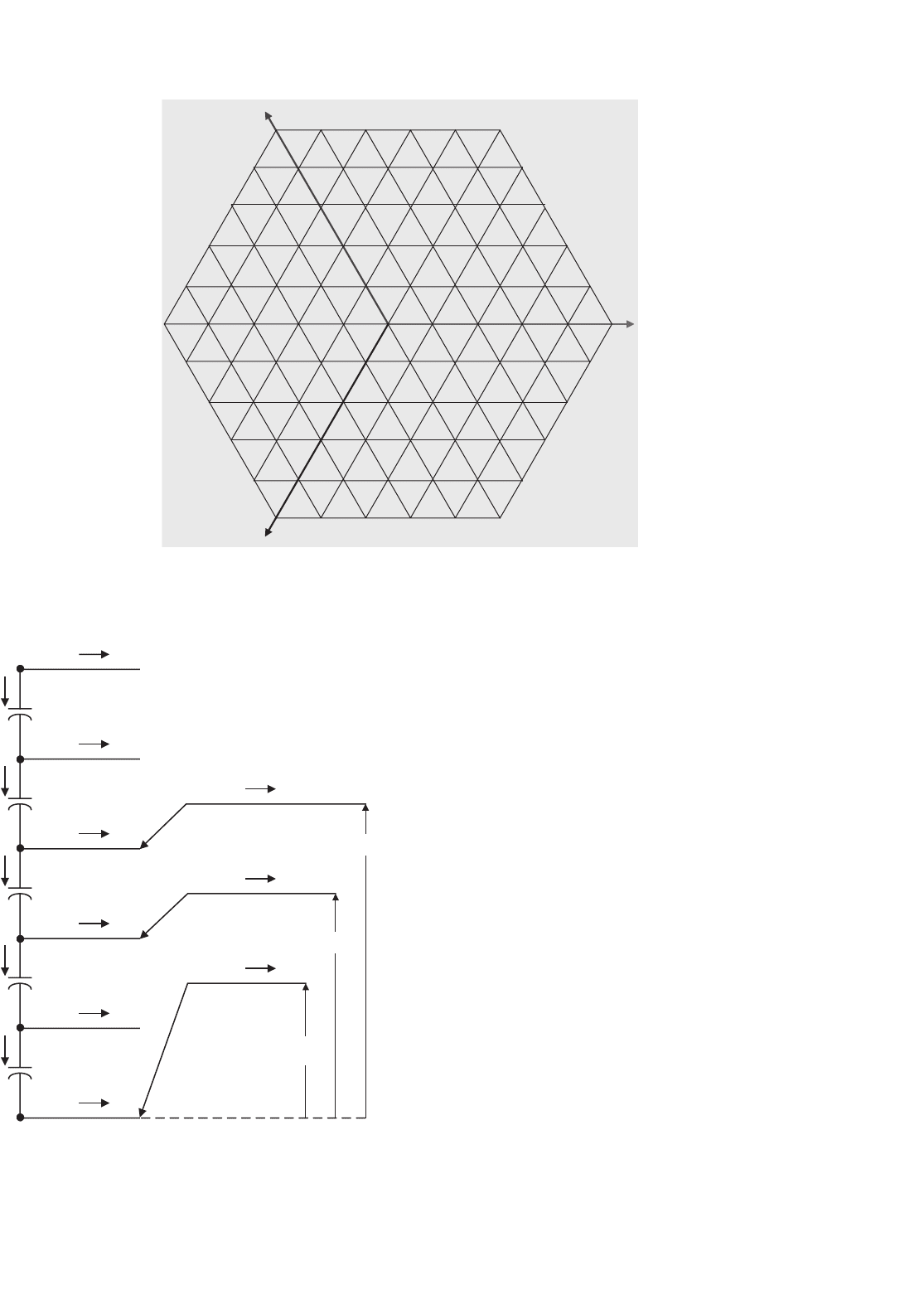
As an example of how to accomplish this doubling of
inverter frequency, an analysis of a seven-level diode-clamped
inverter with an amplitude modulation index of 0.4 is con-
ducted. During one cycle, the reference waveform is centered
in the upper three carrier bands, and during the next cycle,
the reference waveform is centered in the lower three car-
rier bands as shown in Fig. 17.20. This technique enables half
of the switches to “rest” every other cycle and not incur any
switching losses. With this method, the switching frequency
(or carrier frequency f
c
in the case of multilevel inverters) can
effectively be doubled to 2f
c
, but the switches will have the
same thermal losses as if they were switching at f
c
but every
cycle.
17 Multilevel Power Converters 465
TABLE 17.5 Increased switching frequency possible at
lower modulation indices
Inverter
levels
Modulation index, m
a
Frequency
multiplier
Min Max
3 0.000 0.500 2X
4 0.000 0.333 3X
5 0.250 0.500 2X
0.000 0.250 4X
6 0.200 0.400 2X
0.000 0.200 5X
7 0.333 0.500 2X
0.167 0.333 3X
0.000 0.167 6X
8 0.285 0.428 2X
0.142 0.285 3X
0.000 0.142 7X
9 0.25 0.500 2X
0.125 0.250 4X
0.000 0.125 8X
10 0.333 0.444 2X
0.222 0.333 3X
0.111 0.222 4X
0.000 0.111 9X
11 0.333 0.500 2X
0.200 0.333 3X
0.000 0.200 5X
12 0.272 0.454 2X
0.181 0.272 3X
0.090 0.181 5X
0.000 0.090 11X
13 0.333 0.500 2X
0.250 0.333 3X
0.167 0.250 4X
0.0833 0.167 6X
0.000 0.0833 12X
This method is possible only for three-wire systems because
the diode-clamped inverter has line–line redundancies and
no phase redundancies. This means that at the discontinu-
ity where the reference moves from one carrier band set to
another, the transition has to be synchronized such that all
3.0
4.0
5.0
6.0
2.0
1.0
0
time (radians)
voltage (p.u.)
(h
a
= h
a
− 3)
(h
a
= h
a
+ 3)
2π 4π
FIGURE 17.20 Reference rotation among carrier bands at low modulation indices (m
a
< 0.5).
three phases are moved from one carrier set to the next
set at the same time. In the case of frequency doubling, all
three phases add or subtract the following number of states
(or levels) every other reference cycle
h
a
j + 1
= h
a
(j) + (−1)
j
·
m −1
2
(17.11)
At modulation indices closer to zero, the switching fre-
quency can be increased even more. This is possible because
the reference waveform can be rotated among the carrier bands
for a few cycles before returning to a previous set of switches
for use. The switches are allowed to “rest” for a few cycles and
thus are able to absorb higher losses during the cycle that they
are in use. Table 17.5 shows the possible increased switching
frequencies available at lower amplitude modulation indices
for several different inverter levels.
Some additional switching loss is associated with the redun-
dant switchings of the three phases at the end of each
modulation cycle when rotating among carrier bands. For
instance, for Fig. 17.20 each of the three phases in the seven-
level inverter will have three switch pairs change states at the
end of every reference cycle. Compared to the switching loss
associated with just the normal PWM switchings, however,
this redundant switching loss is quite small, typically less than
5% of the total switching loss.
Figures 17.21 and 17.22 illustrate two different methods
of rotating the reference waveform among three different
regions (top, middle, and bottom) for modulation indices
less than 0.333 in a seven-level inverter to enable the car-
rier frequency to be increased by a factor of three. The
method shown in Fig. 17.21 is preferred over that shown
in Fig. 17.22 because of less redundant state switching. The
method in Fig. 17.21 requires only four redundant state switch-
ings for every three reference cycles, whereas the method
in Fig. 17.22 requires eight redundant switchings for every
three reference cycles. In general for any multilevel inverter
regardless of the number of levels or number of rotation
regions, using the preferred reference rotation method will
466 S. Khomfoi and L. M. Tolbert
3.0
4.0
5.0
6.0
2.0
1.0
0
time (radians)
voltage (p.u.)
2π 4π 8π 10π 14π
(h
a
=h
a
−2) (h
a
=h
a
−2) (h
a
=h
a
+2) (h
a
=h
a
+2) (h
a
=h
a
−2)
top region
bottom region
middle region
FIGURE 17.21 Preferred method of reference rotation among carrier bands with 3× carrier frequency at very low modulation indices.
time (radians)
voltage (p.u.)
2π 4π 6π 8π 10π 12π 14π
(h
a
=h
a
−2)
(h
a
=h
a
−2) (h
a
=h
a
−2) (h
a
=h
a
−2)
(h
a
=h
a
−2)
top region
bottom region
(h
a
=h
a
+4) (h
a
=h
a
+4)
middle region
3.0
3.0
5.0
6.0
2.0
1.0
0
FIGURE 17.22 Alternate method of reference rotation among carrier bands with 3× carrier frequency at very low modulation indices.
have 1/2 of the redundant switching losses that the alternate
method would have.
Unlike the diode-clamped inverter, the cascaded H-bridges
inverter has phase redundancies in addition to the
aforementioned line–line redundancies. Phase redundancies
are much easier to exploit than line–line redundancies because
the output voltage in each phase of a three-phase inverter can
be generated independently of the other two phases when only
phase redundancies are used. A method was given in [18]
that makes use of these phase redundancies in a cascaded
inverter so that each active device’s duty cycle is balanced
over (m − 1)/2 modulation waveform cycles regardless of the
modulation index. The same pulse rotation technique used
for fundamental frequency switching of cascade inverters was
used but with a PWM output voltage waveform [55], which
is a much more effective means of controlling a driven motor
at low speeds than continuing to do fundamental frequency
switching. The effect of this control is that the output wave-
form can have a high switching frequency but the individual
levels can still switch at a constant switching frequency of
60 Hz, if desired.
17.3.2 Multilevel Space Vector PWM
Choi [56] was the first author to extend the two-level space
vector PWM technique to more than three levels for the
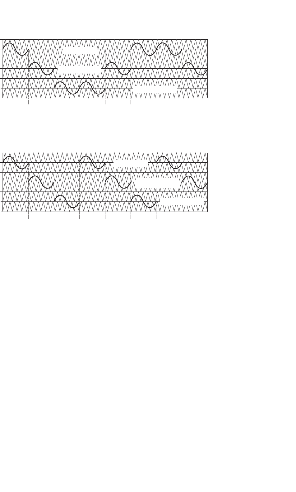
diode-clamped inverter. Figure 17.23 shows what the space
vector d–q plane looks like for a six-level inverter. Figure 17.24
represents the equivalent dc link of a six-level inverter as a mul-
tiplexer that connects each of the three output phase voltages
to one of the dc link voltage tap points [57]. Each integral point
on the space vector plane represents a particular three-phase
output voltage state of the inverter. For instance, the point
(3, 2, 0) on the space vector plane means, that with respect to
ground, a phase is at 3V
dc
, b phase is at 2V
dc
, and c phase is
at 0V
dc
. The corresponding connections between the dc link
and the output lines for the six-level inverter are also shown in
Fig. 17.24 for the point (3, 2, 0). An algebraic way to represent
the output voltages in terms of the switching states and dc link
capacitors is described in the following [58]. For n = m−1,
where m is the number of levels in the inverter
V
abc0
= H
abc
V
c
(17.12)
17 Multilevel Power Converters 467
0,5,0
0,0,0 1,0,0 2,0,0 3,0,0 4,0,0 5,0,0
0,1,0 1,1,0 2,1,0 3,1,0 4,1,0 5,1,0
0,2,0 1,2,0 2,2,0 3,2,0 4,2,0 5,2,0
0,3,0 1,3,0 2,3,0 3,3,0 4,3,0 5,3,0
0,4,0 1,4,0 2,4,0 3,4,0 4,4,0 5,4,0
1,5,0 2,5,0 3,5,0 4,5,0
5,5,0
0,0,1 1,0,1 2,0,1 3,0,1 4,0,1 5,0,1
0,0,2 1,0,2 2,0,2 3,0,2 4,0,2 5,0,2
0,0,3 1,0,3 2,0,3 3,0,3 4,0,3 5,0,3
0,0,4 1,0,4 2,0,4 3,0,4 4,0,4 5,0,4
0,0,5 1,0,5 2,0,5 3,0,5 4,0,5 5,0,5
0,5,5 0,4,4 0,3,3 0,2,2 0,1,1
0,4,5 0,3,4 0,2,3 0,1,2
0,3,5 0,2,4 0,1,3
0,2,5 0,1,4
0,1,5
0,5,3 0,4,2 0,3,1
0,5,2 0,4,1
0,5,1
0,2,10,5,4 0,4,3 0,3,2
a
c
b
FIGURE 17.23 Voltage space vectors for a six-level inverter.
0
i
L0
i
L1
i
L2
i
L3
i
L4
i
L5
i
c5
i
c4
i
c3
i
c2
i
c1
i
Lc
i
Lb
i
La
v
Lc0
v
Lb0
v
La0
v
c5
v
c4
v
c3
v
c2
v
c1
h
a
=3
h
b
=2
h
c
=0
FIGURE 17.24 Multiplexer model of diode-clamped six-level inverter.
where,
V
c
=
V
c1
V
c2
V
c3
... V
cn
T
;
H
abc
=
h
a1
h
a2
h
a3
... h
an
h
b1
h
b2
h
b3
... h
bn
h
c1
h
c2
h
c3
... h
cn
; V
abc0
=
V
a0
V
b0
V
c0
and
h
aj
=
n
j
δ(h
a
−j)
where h
a
is the switch state and j is an integer from 0 to n, and
where δ(x)=1ifx ≥ 0, δ(x) = 0ifx < 0.
Besides the output voltage state, the point (3, 2, 0) on the
space vector plane can also represent the switching state of the
converter. Each integer indicates how many upper switches in
each phase leg are on for a diode-clamped converter. As an
example, for h
a
= 3, h
b
= 2, h
c
= 0, the H
abc
matrix for this
particular switching state of a six-level inverter would be
H
abc
=
00111
00011
00000
468 S. Khomfoi and L. M. Tolbert
Redundant switching states are those states for which a par-
ticular output voltage can be generated by more than one
switch combination. Redundant states are possible at lower
modulation indices, or at any point other than those on the
outermost hexagon shown in Fig. 17.23. Switch state (3, 2, 0)
has redundant states (4, 3, 1) and (5, 4, 2). Redundant switch-
ing states differ from each other by an identical integral value,
i.e. (3, 2, 0) differs from (4, 3, 1) by (1, 1, 1) and from (5, 4, 2)
by (2, 2, 2).
For an output voltage state (x, y, z) in an m-level diode-
clamped inverter, the number of redundant states available
is given by m − 1 − max(x, y, z). As the modulation index
decreases (or the voltage vector in the space vector plane
gets closer to the origin), more redundant states are available.
The number of possible zero states is equal to the number of
levels, m. For a six-level diode-clamped inverter, the zero volt-
age states are (0, 0, 0), (1, 1, 1), (2, 2, 2), (3, 3, 3), (4, 4, 4),
and (5, 5, 5).
The number of possible switch combinations is equal to the
cube of the level (m
3
). For this six-level inverter, there are 216
possible switching states. The number of distinct or unique
states for an m-level inverter can be given by
m
3
−
(
m −1
)
3
=
6
m−1
n=1
n
+1 (17.13)
Therefore, the number of redundant switching states for
an m-level inverter is (m − 1)
3
. Table 17.6 summarizes the
available redundancies and distinct states for a six-level diode-
clamped inverter.
In two-level PWM, a reference voltage is tracked by selecting
the two nearest voltage vectors and a zero vector and then by
calculating the time required to be at each of these three vectors
such that their sum equals the reference vector. In multilevel
PWM, generally the nearest three triangle vertices, V
1
, V
2
, and
TABLE 17.6 Line–line redundancies of six-level three-phase diode-
clamped inverter
Redundancies Distinct
states
Redundant
states
Unique state coordinates: (a, b, c)
where 0 ≤a, b, c ≤5
5 1 5 (0,0,0)
4 6 24 (0,0,1),(0,1,0),(1,0,0),(1,0,1),(1,1,0),
(0,0,1)
3 12 36 (p,0,2),(p,2,0),(0,p,2),(2,p,0),(0,2,p,),
(2,0,p) where p ≤2
2 18 36 (0,3,p),(3,0,p),(p,3,0),(p,0,3),(3,p,0),
(0,p,3) where p ≤3
1 24 24 (0,4,p),(4,0,p),(p,4,0),(p,0,4),(4,p,0),
(0,p,4) where p ≤4
0 30 0 (0,5,p),(5,0,p),(p,5,0),(p,0,5),(5,p,0),
(0,p,5) where p ≤5
Total 91 125 216 total states
V
3
, to a reference point V
∗
are selected so as to minimize the
harmonic components of the output line–line voltage [59].
The respective time duration, T
1
, T
2
, and T
3
, required of these
vectors is then solved from the following equations
V
1
T
1
+
V
2
T
2
+
V
3
T
3
= V
∗
T
s
(17.14)
T
1
+T
2
+T
3
= T
s
(17.15)
where T
s
is the switching period. Equation (17.14) actually
represents two equations, one with the real part of the terms
and one with the imaginary part of the terms
V
1d
T
1
+V
2d
T
2
+V
3d
T
3
= V
∗
d
T
s
(17.16)
V
1q
T
1
+V
2q
T
2
+V
3q
T
3
= V
∗
q
T
s
(17.17)
Equations (17.15) – (17.18) can then be solved for T
1
, T
2
, and
T
3
as follows:
T
1
T
2
T
3
=
V
1d
V
2d
V
3d
V
1q
V
2q
V
3q
111
−1
V
∗
d
T
s
V
∗
q
T
s
T
s
(17.18)
Others have proposed space vector methods that did not
use the nearest three vectors, but these methods generally add
complexity to the control algorithm. Figure 17.25 shows what
a sinusoidal reference voltage (circle of points) and the inverter
output voltages look like in the d–q plane.
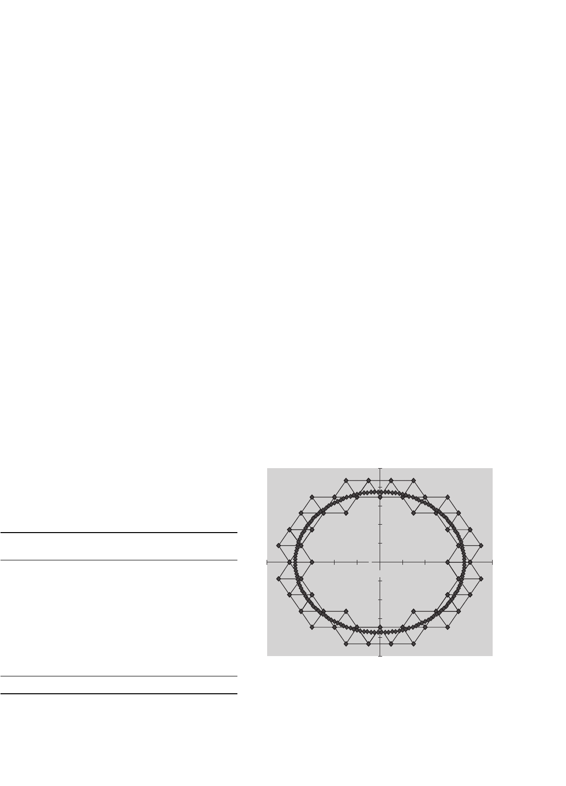
Redundant switch levels can be used to help manage the
charge on the dc link capacitors [60]. Generalizing from
0
–5
–4
–3
–2
–1
1
2
3
4
5
–5 –4 –3 –2 –1 1 2 3 4 5
d
q
0
FIGURE 17.25 Sinusoidal reference and inverter output voltage states
in d–q plane.