Power electronic handbook
Подождите немного. Документ загружается.


17 Multilevel Power Converters 469
Fig. 17.24, the equations for the currents through the dc link
capacitors can be given as
i
cn
=−i
Ln
(17.19)
and
i
c(n−j)
=−i
L(n−j)
+i
c(n−j+1)
, where j = 1, 2, 3, ..., n −1
(17.20)
The dc link currents for h
a
= 3, h
b
= 2, h
c
= 0 would be
i
c5
= i
c4
= 0, i
c3
=−i
a
, i
c2
=−i
a
−i
b
, i
c1
=−i
a
−i
b
. To see
how redundant states affect the dc link currents, consider the
two redundant states for (3, 2, 0). In state (4, 3, 1), the dc
link currents would be i
c5
= 0, i
c4
=−i
a
, i
c3
=−i
a
− i
b
,
i
c2
=−i
a
−i
b
, i
c1
=−i
a
−i
b
−i
c
= 0; and for the state (5, 4, 2),
the dc link currents would be i
c5
=−i
a
, i
c4
=−i
a
− i
b
,
i
c3
=−i
a
−i
b
, i
c2
= i
c1
=−i
a
−i
b
−i
c
= 0.
From this example, one can see that the choice of redundant
switching states can be used to determine which capacitors
will be charged/discharged or unaffected during the switching
period. While this control is helpful in balancing the individ-
ual dc voltages across the capacitors that make up the dc link,
this method is quite complicated in selecting which of the
redundant states to use. Constant use of redundant switch-
ing states also results in a higher switching frequency and
lower efficiency of the inverter because of the extra switch-
ings. Recently, optimized space vector switching sequences for
multilevel inverters have been proposed in [61].
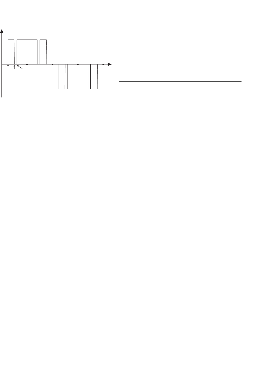
17.3.3 Selective Harmonic Elimination
A. Fundamental Switching Frequency
The selective harmonic elimination method is also called
fundamental switching frequency method based on the har-
monic elimination theory proposed by Patel [62, 63]. A typical
11-level multilevel converter output with fundamental fre-
quency switching scheme is shown in Fig. 17.2. The Fourier
series expansion of the output voltage waveform as shown in
Fig. 17.2 is expressed in Eqs. (17.1) and (17.2).
The conducting angles, θ
1
, θ
2
, ..., θ
s
, can be chosen such that
the voltage total harmonic distortion is a minimum. Normally,
these angles are chosen so as to cancel the predominant lower
frequency harmonics [19].
For the 11-level case in Fig. 17.2, the 5th, 7th, 11th, and
13th harmonics can be eliminated with the appropriate choice
of the conducting angles. One degree of freedom is used so
that the magnitude of the fundamental waveform corresponds
to the reference waveform’s amplitude or modulation index,
m
a
, which is defined as V
∗
L
/V
Lmax
. V
∗
L
is the amplitude com-
mand of the inverter for a sine wave output phase voltage, and
V
Lmax
is the maximum attainable amplitude of the converter,
i.e. V
Lmax
= s · V
dc
. The equations from Eq. (17.2) will now
be as follows
cos
(
5θ
1
)
+cos
(
5θ
2
)
+cos
(
5θ
3
)
+cos
(
5θ
4
)
+cos
(
5θ
5
)
=0
cos
(
7θ
1
)
+cos
(
7θ
2
)
+cos
(
7θ
3
)
+cos
(
7θ
4
)
+cos
(
7θ
5
)
=0
cos
(
11θ
1
)
+cos
(
11θ
2
)
+cos
(
11θ
3
)
+cos
(
11θ
4
)
+cos
(
11θ
5
)
=0
cos
(
13θ
1
)
+cos
(
13θ
2
)
+cos
(
13θ
3
)
+cos
(
13θ
4
)
+cos
(
13θ
5
)
=0
cos
(
θ
1
)
+cos
(
θ
2
)
+cos
(
θ
3
)
+cos
(
θ
4
)
+cos
(
θ
5
)
=5m
a
(17.21)
The above equations are non-linear transcendental equations
that can be solved by an iterative method such as the Newton–
Raphson method. For example, using a modulation index of
0.8 obtains: θ
1
= 6.57
◦
, θ
2
= 18.94
◦
, θ
3
= 27.18
◦
, θ
4
= 45.14
◦
,
θ
5
= 62.24
◦
. Thus, if the inverter output is symmetrically
switched during the positive half cycle of the fundamental
voltage to +V
dc
at 6.57
◦
, +2V
dc
at 18.94
◦
, +3V
dc
at 27.18
◦
,
+4V
dc
at 45.14
◦
, and +5V
dc
at 62.24
◦
, and similarly in the neg-
ative half cycle to −V
dc
at 186.57
◦
, −2V
dc
at 198.94
◦
, −3V
dc
at 207.18
◦
, −4V
dc
at 225.14
◦
, −5V
dc
at 242.24
◦
, the output
voltage of the 11-level inverter will not contain the 5th, 7th,
11th, and 13th harmonic components [18]. Other methods
to solve these equations include using genetic algorithms [64]
and resultant theory [65–67].
Practically, the precalculated switching angles are stored as
the data in memory (look-up table). Therefore, a microcon-
troller could be used to generate the PWM gate drive signals.
B. Selective Harmonic Elimination PWM
In order to achieve a wide range of modulation indexes with
minimized THD for the synthesized waveforms, a generalized
selective harmonic modulation method [68, 69] was proposed,
which is called virtual stage PWM [64]. An output waveform
is shown in Fig. 17.26. The virtual stage PWM is a combi-
nation of unipolar programmed PWM and the fundamental
frequency switching scheme. The output waveform of unipolar
programmed PWM is shown in Fig. 17.27. When unipolar
3p/2
p/2
0
2pp
q
1
q
2
q
3
q
4
FIGURE 17.26 Output waveform of virtual stage PWM control.
470 S. Khomfoi and L. M. Tolbert
0
–V
dc
V
dc
T/4 T/2
3T/2 T
t
q
1
q
2
q
3
FIGURE 17.27 Unipolar switching output waveform.
programmed PWM is employed on a multilevel converter,
typically one dc voltage is involved, where the switches con-
nected to the dc voltage are switched “on” and “off” several
times per fundamental cycle. The switching pattern decides
what the output voltage waveform looks like.
For fundamental switching frequency method, the num-
ber of switching angles is equal to the number of dc sources.
However, for the virtual stage PWM method, the number of
switching angles is not equal to the number of dc voltages. For
example, in Fig. 17.26, only two dc voltages are used, whereas
there are four switching angles.
Bipolar programmed PWM and unipolar programmed
PWM could be used for modulation indices, too low for the
applicability of the multilevel fundamental frequency switch-
ing method. Virtual stage PWM can also be used for low
modulation indices. Virtual stage PWM will produce output
waveforms with a lower THD most of the time [64]. There-
fore, virtual stage PWM provides another alternative to bipolar
programmed PWM and unipolar programmed PWM for low
modulation index control.
The major difficulty for selective harmonic elimination
methods, including the fundamental switching frequency
method and the virtual stage PWM method, is to solve the
transcendental Eq. (17.21) for switching angles. Newton’s
method can be used to solve Eq. (17.21), but it needs good
initial guesses, and solutions are not guaranteed. Therefore,
Newton’s method is not feasible to solving equations for large
number of switching angles if good initial guesses are not
available [70].
Recently, the resultant method has been proposed in
[65–67] to solve the transcendental equations for switching
angles. The transcendental equations characterizing the har-
monic content can be converted into polynomial equations.
Elimination resultant theory has been employed to determine
the switching angles to eliminate specific harmonics, such
as the 5th, 7th, 11th, and 13th. However, as the number of
dc voltages or the number of switching angles increases, the
degrees of the polynomials in these equations become bulky.
To conquer this problem, the fundamental frequency switch-
ing angle computation is solved by Newton’s method. The
initial guess can be provided by the results of lower order
transcendental equations by the resultant method [70].
17.4 Multilevel Converter Design
Example
The objective of this section is to give a general idea how to
design a multilevel converter in a specific application. Differ-
ent applications for multilevel converters might have different
specification requirements. Therefore, the multilevel universal
power conditioner (MUPC) is utilized to demonstrate as the
design example in this section.
Multilevel diode clamped converters can be designed where
different levels have unequal voltage and current ratings; how-
ever, this approach would lose the advantage of being able to
use identical, modular units for each leg of the inverter. The
method used in this chapter to specify a back-to-back diode
clamped converter for use as a universal power conditioner is
for all voltage levels and legs in each of the two inverters to
be the same. (The current ratings in the series inverter may
be different than those in the parallel inverter.) This approach
also allows the control system to extend the frequency range of
the inverter by exploiting the additional voltage redundancies
available at lower modulation indices as discussed in [71].
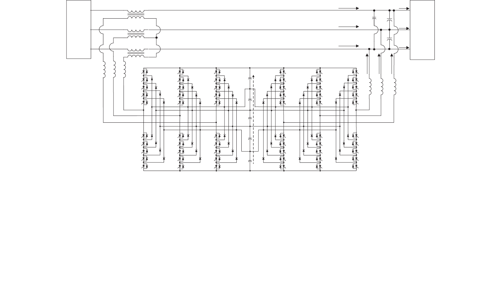
17.4.1 Interface with Electrical System
Figure 17.28 illustrates the proposed electrical system con-
nection topology for two diode-clamped inverters connected
back-to-back and sharing a common dc bus. One inverter
interfaces with the electrical system by means of a parallel
connection through output inductors L
PI
. The other inverter
interfaces with the electrical system through a set of single-
phase transformers in a series fashion. The primaries of the
transformers are inserted in series with each of the three phase
conductors supplied from a utility. The secondaries of the
transformers are connected in an ungrounded wye and to
the output of the series inverter. By having two inverters, this
arrangement allows both the source voltage and the load cur-
rent to be compensated independently of each other [71, 72].
With only a single inverter, regulating the load voltage and
source current at the same time would not be possible.
The voltage injected into the electrical system by the series
inverter compensates for deviations in the source voltage such
that a regulated distortion-free waveform is supplied to the
load. The parallel inverter injects current into the electrical
system to compensate for current harmonics and/or reactive
current demanded by the load such that the current drawn
from the utility is in phase with the source voltage and contains
no harmonic components.
17 Multilevel Power Converters 471
VLb
V
Lc
C
p
C
p
C
p
V5
V4
V3
V2
V1
C4
C3
C2
C1
V6
C5
Sa1
Sa2
Sa3
Sa4
D1
D2
D3
Sa5
D4
Sa'1
Sa'2
Sa'3
Sa'4
D4
D3
D2
Sa'5
D1
Sb1
Sb2
Sb3
Sb4
D1
D2
D3
Sb5
D4
Sb'1
Sb'2
Sb'3
Sb'4
D4
D3
D2
Sb'5
D1
Sc1
Sc2
Sc3
Sc4
D1
D2
D3
Sc5
D4
Sc'1
Sc'2
Sc'3
Sc'4
D4
D3
D2
Sc'5
D1
Sa1
Sa2
Sa3
Sa4
D1
D2
D3
Sa5
D4
Sa'1
Sa'2
Sa'3
Sa'4
D4
D3
D2
Sa'5
D1
Sb1
Sb2
Sb3
Sb4
D1
D2
D3
Sb5
D4
Sb'1
Sb'2
Sb'3
Sb'4
D4
D3
D2
Sb'5
D1
Sc1
Sc2
Sc3
Sc4
D1
D2
D3
Sc5
D4
Sc'1
Sc'2
Sc'3
Sc'4
D4
D3
D2
Sc'5
D1
5V
dc
series inverter
parallel inverter
0
V
Sb
Source
(Utility)
V
Sa
V
Sc
I
PIb
I
PIc
I
PIa
I
Lc
I
La
I
Lb
V
La
Load
I
Sa
I
Sb
I
Sc
L
PIc
L
PIa
L
PIb
L
SI
L
SI
L
SI
FIGURE 17.28 Electrical system connection of multilevel diode-clamped power conditioner.

472 S. Khomfoi and L. M. Tolbert
17.4.2 Number of Levels and Voltage Rating of
Active Devices
In a multilevel inverter, determining the number of levels will
be one of the most important factors because this affects many
of the other sizing factors and control techniques. Tradeoffs, in
specifying the number of levels that the power conditioner will
need and the advantages and complexity of having multiple
voltage levels available, are the primary differences that set a
multilevel filter apart from a single level filter.
As a starting point, known is the nominal RMS voltage rat-
ing, V
nom
, of the electrical system to which the diode-clamped
power conditioner will be connected. The dc link voltage must
be at least as high as the amplitude of the nominal line–neutral
voltage at the point of connection, or
√
2 ·V
nom
.
The parallel inverter must be able to inject currents by
imposing a voltage across the parallel inductors, L
PI
, that is
the difference between the load voltage V
L
and parallel inverter
output voltage V
PI
. The most difficult time to impose a volt-
age across the inductors is when the load voltage waveform is
at its maximum or minimum. Simulation results have shown
that the amplitude of the desired load voltage V
nom
should
not be more than 70% of the overall dc link voltage for the
parallel inverter to have sufficient margin to inject appropriate
compensation currents. Without this margin, complete com-
pensation of reactive currents may not be possible. This margin
can be incorporated into a design factor for the inverter.
Because, the dc link voltage and the voltage at the connec-
tion point, both can vary, the design factor used in the rating
selection process incorporates these elements as well as the
small voltage drops that occur in the inverters during active
device conduction.
The product of the number of the active devices in series
(m − 1) and the voltage rating of the devices V
dev
must then
be such that
V
device
rating
·
(
m −1
)
≥
√
2 ·V
nom
·D
design
factor
(17.22)
The minimum number of levels and the voltage rating of
the active devices (IGBTs, GTOs, power MOSFETs, etc.) are
inversely related to each other. More levels in the inverter will
lower the required voltage device rating of individual devices,
or looking at it another way, a higher voltage rating of the
devices will enable a fewer minimum number of levels to be
used.
Increasing the number of levels does not affect the total
voltage blocking capability of the active devices in each phase
leg because lower device ratings can be used. Some of the
benefits of using more than the minimum required number of
levels in a diode-clamped inverter are as follows:
1. Voltage stress across each device is lower. Both active
devices and dc link capacitors could be used that
have lower voltage ratings (which sometimes are much
cheaper and have greater availability).
2. The inverter will have a lower EMI because the dv/dt
during each switching will be lower.
3. The output of the waveform will have more steps,
or degrees of freedom, which enables the output
waveform to closely track a reference waveform.
4. Lower individual device switching frequency will
achieve the same results as an inverter with a fewer
number of levels and higher device switching fre-
quency. Or the switching frequency can be kept the
same as that in an inverter with a fewer number of
levels to achieve a better waveform.
The drawbacks of using more than the required minimum
number of levels are as follows:
1. Six active device control signals (one for each phase
of the parallel inverter and the series inverter) are
needed for each hardware level of the inverter –
i.e. 6 ·(m −1) control signals. Additional levels require
more computational resources and add complexity to
the control.
2. If the blocking diodes used in the inverter have
the same rating as the active devices, their number
increases dramatically because 6·(m−2)·(m−1) diodes
would be required for the back-to-back structure.
Considering the tradeoffs between the number of levels and
the voltage rating of the devices will generally lead the designer
to choose an appropriate value for each.
17.4.3 Number and Voltage Rating of Clamping
Diodes
As shown in the previous section, 6·(m −1)·(m −2) clamping
diodes are required for an m-level back-to-back converter if
the diodes have the same voltage rating as the active devices.
As discussed in Section 17.2, the voltage rating of each series
of clamping diodes is designated by the subscript of the diode
shown in Fig. 17.28. For instance, D
4
must block 4V
dc
,D
3
must block 3V
dc
, and so on.
If diodes that have higher voltage ratings than the active
devices are available, then the number of diodes required can
be reduced accordingly. When considering diodes of differ-
ent ratings, the minimum number of clamping diodes per
phase leg of the inverter is 2 · (m − 2) and for the complete
back-to-back converter, 12·(m −2). Unlike the active devices,
additional levels do not enable a decrease in the voltage rating
of the clamping diodes. In each phase leg, note that the volt-
age rating of each pair of diodes adds up to the overall dc link
voltage (m − 1) · V
dc
. Considering the six-level converter in
Fig. 17.28, connected to voltage level V
5
are the anode of D
1
and the cathode of D
4
.D
1
must be able to block V
dc
, and D
4
17 Multilevel Power Converters 473
must block 4V
dc
, the sum of their voltage blocking capabilities
is 5V
dc
. For voltage level V
4
, the anode of D
2
and the cathode
of D
3
are connected together to this point. Again, the sum
of their voltage blocking capability is 2V
dc
+ 3V
dc
= 5V
dc
.
The same is true for the other intermediate voltage levels.
Therefore, the total voltage blocking capability per phase of
an m-level converter is (m − 2) · (m − 1) · V
dc
and for the
back-to-back converter,
V
clamp
total
= 6 ·
(
m −2
)
·
(
m −1
)
·V
dc
(17.23)
Each additional level added to the converter will require an
additional 6 · (m − 1) · V
dc
in voltage blocking capabilities.
From this, one can see that unnecessarily adding more than
the required number of voltage levels can quickly become cost
prohibitive.
17.4.4 Current Rating of Active Devices
In order to determine the required current rating of the active
switching devices for the parallel and series portions of the
back-to-back converter shown in Fig. 17.28, the maximum
apparent power that each inverter will either supply or draw
from the electrical system must be known. These ratings will
largely depend on the compensation objectives and to what
limits they are specified to maintain. Of the three voltage com-
pensation objectives (voltage sag, unbalanced voltages, voltage
harmonics), the greatest power demands of the series inverter
will almost always occur during voltage sag conditions. For
the parallel inverter, generally the reactive power compensa-
tion demands will dominate the design of the converter, as
opposed to harmonic current compensation.
For this analysis, balanced voltage sag conditions will be
considered in the specification of the power ratings of the two
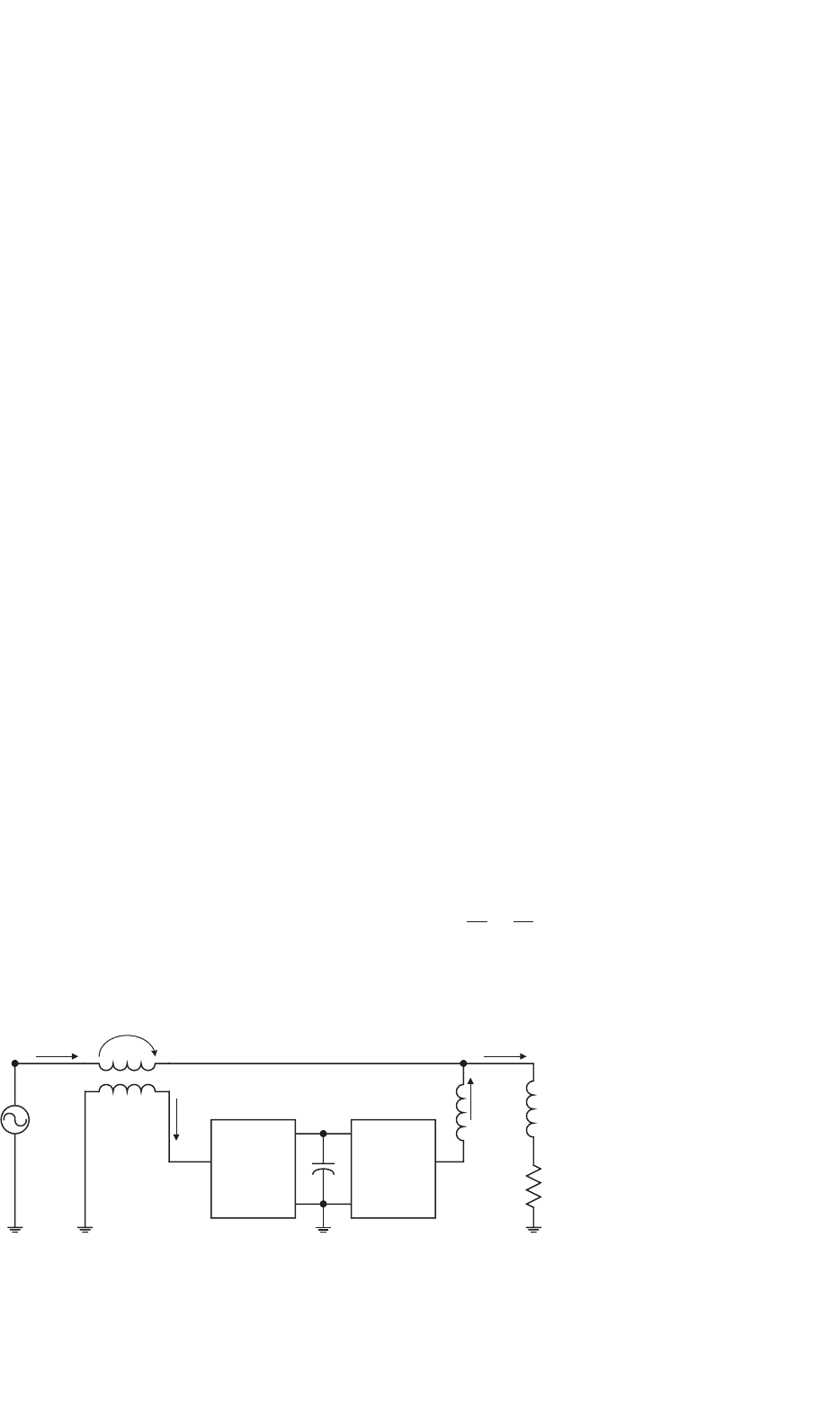
inverters. A one-line diagram circuit is shown in Fig. 17.29 for
the converter and electrical system represented in Fig. 17.28.
Equations can be developed for the apparent power required
of each of the inverters based on the three phase rated apparent
Parallel
Inverter
Series
Inverter
V
L
i
L
i
PI
i
S
V
S
V
SI
i
SI
(m−1)V
DC
L
PI
FIGURE 17.29 One-line diagram of a MUPC connected to the electrical system.
load power S
Lnom
, rated line–line load voltage V
Lnom
, and line–
line source voltage V
S
[73].
A. Series Inverter Power Rating
First, the rating of the series inverter will be considered. The
voltage V
SI
across the series transformer shown in Fig. 17.29,
is given by the vector equation
V
SI
=
V
L
−
V
S
(17.24)
The apparent power delivered from the series converter can
then be given as
S
SI
=
V
L
−
V
S
·
I
∗
S
(17.25)
where
I
∗
S
is the conjugate of
I
S
, the source current.
If the load voltage V
L
is regulated such that it is in phase
with the source voltage V
S
, then Eq. (17.24) can be rewritten
as an algebraic equation
V
SI
= V
L
−V
S
(17.26)
Assuming that the back-to-back converter is lossless, the
entire real power P
L
drawn by the load must be supplied by
the utility source, P
S
= P
L
. If the source current is regulated
such that it is in phase with the source voltage, then
P
S
= V
S
·I
S
= P
L
(17.27)
Combining Eqs. (17.25)–(17.27), the real power delivered
from the series converter is
P
SI
= (V
L
−V
S
) ·I
S
(17.28)
Multiplying and dividing the right side of Eq. (17.28) by V
s
yields
P
SI
=
V
L
V
S
−
V
S
V
S
·I
S
·V
S
(17.29)

474 S. Khomfoi and L. M. Tolbert
Substituting Eq. (17.27) into Eq. (17.29) produces the fol-
lowing equation for the rated apparent power of the series
inverter
S
SI
= P
SI
= P
L
·
V
L
V
S
−1
(17.30)
Choosing the rated load power S
L
and the rated load voltage
V
L
as bases, Fig. 17.30 shows the apparent power S
SI
in per
unit that the series inverter must provide as a function of the
source voltage V
S
. Each of the curves in Fig. 17.30 is for loads
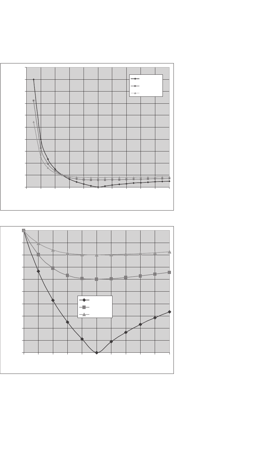
of different power factors. As shown in Fig. 17.30, the apparent
power that the series inverter has to transfer is proportional to
the power factor of the load [73].
Figure 17.30a shows that for voltage sags less than 50% of
nominal, the series inverter would have to be rated to transfer
more power than the rated load power, which in most applica-
tions would not be practical. Figure 17.30b shows that for sags
that are small in magnitude, the series inverter would have a
rating much less than that of the rated load power. For exam-
ple, for a 20% voltage sag (V
s
= 0.8·V
nom
), the required power
rating of the series inverter is only 25% of the rated load.
When considering selection of the active devices for the
series inverter, as shown in Fig. 17.30, the magnitude of
the voltage sag to be compensated will play a large role in
determining the current rating required. The formula for
determining the current rating of each of the devices as a
function of the minimum source voltage to be compensated,
min(V
s
), is given in Eq. (17.31)
I
SI
device
rating
=
S
Lnom
·
((
V
nom
)
/
(
V
nom
−min
(
V
S
))
−1
)
√
3 ·V
nom
·D
safety
factor
(17.31)
The safety factor, or design factor, in Eq. (17.31) should be
chosen to allow for future growth in the load supplied by the
utility and compensated by the power conditioner.
B. Parallel Inverter Power Rating
The power rating of the parallel inverter will now be consid-
ered. From Fig. 17.29, the apparent power delivered to the
electrical system by the parallel inverter can be expressed as
S
PI
=
S
L
−
V
L
·
I
∗
S
=
P
L
+jQ
L
−V
L
I
S
(17.32)
because the source current I
s
and load voltage V
L
are con-
trolled such that they are in phase with the source voltage [73].
Multiplying and dividing the second term of Eq. (17.32) by V
S
and substituting Eq. (17.27) yields the following
V
L
·I
S
=
V
L
V
S
·V
S
I
S
=
V
L
V
S
·P
L
(17.33)
Substituting Eq. (17.33) into Eq. (17.32) and combining like
terms yields
S
PI
= P
L
·
1 −
V
L
V
S
+jQ
L
(17.34)
Figure 17.31 shows the apparent power S
PI
in per unit that
the parallel inverter must provide as a function of the source
voltage V
S
for loads of different power factors. Because the
power transferred for voltage dips to less than 50% of nominal
is predominantly real power, the parallel inverter would have
to have an extraordinarily high rating if the conditioner were
designed to compensate for such large voltage sags, just like
the series inverter. From Fig. 17.31b, one can see that for a
voltage sag to 50% of nominal, the parallel inverter has to
draw a current I
PI
equal to that drawn by the rated load, I
L
.
Unlike the series inverter, however, the dominant factor in
determining the power rating of the parallel inverter is the
load power factor if the conditioner is designed to compensate
for only marginal voltage sags as shown in Fig. 17.31b.
If the design of the universal power conditioner is to com-
pensate for voltage sags to less than 50% of nominal voltage,
then Eq. (17.31) should be used to determine the current rat-
ing of the parallel inverter. If the design of the conditioner is
for marginal voltage sags (to 70% of nominal voltage) and the
MUPC will be applied to a customer load that has a power fac-
tor of less than 0.9, then the following equation is more suited
for calculating the current rating of the parallel inverter’s active
devices
I
PI
device
rating
=
Q
Lnom
√
3·V
nom
·D
design
factor
=
S
Lnom
·
1−
p.f .
2
1/2
√
3·V
nom
·D
design
factor
(17.35)
One common design for the parallel inverter in a universal
power conditioner is for the inverter to have a current rating
equal to that of the rated load current I
L
.
17.4.5 Current Rating of Clamping Diodes
When a multilevel inverter outputs an intermediate voltage
level, not 0 or (m −1) ·V
dc
, only one clamping diode in each
phase leg conducts current at any instant in time whereas half
of the active switches are conducting at all times. The diode
which is conducting current is determined by the intermediate
dc voltage level which is connected to the output phase con-
ductor and by the direction of the current flowing, positive or
negative. For instance, when a phase leg of the series inverter
in Fig. 17.28 is connected to level V
4
, then diode D
2
conducts
for current flowing from the inverter to the electrical system,
and diode D
3
conducts for current flowing into the inverter
from the electrical system.
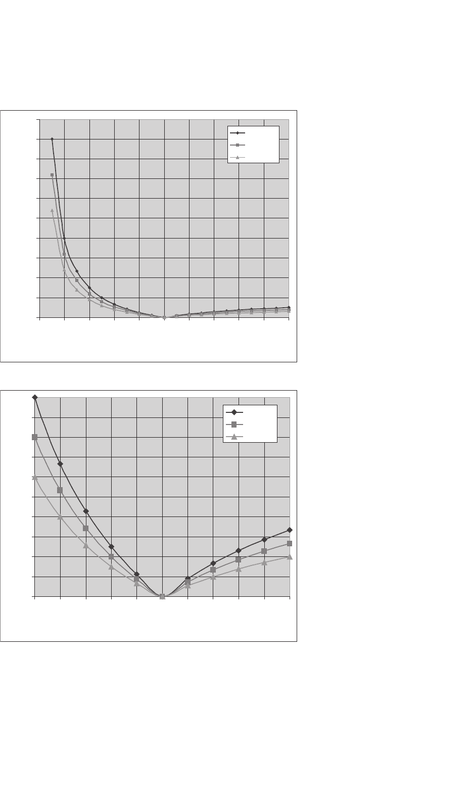
17 Multilevel Power Converters 475
0.0
1.0
2.0
3.0
4.0
5.0
6.0
7.0
8.0
9.0
10.0
0.0 0.2 0.4 0.6 0.8 1.0 1.2 1.4 1.6 1.8 2.0
Source Voltage, V
s
(p.u.)
Power Transferred by Series Inverter, S
SI
(p.u.)
p.f.=1.0
p.f.=0.8
p.f.=0.6
(a)
0.0
0.1
0.2
0.3
0.4
0.5
0.6
0.7
0.8
0.9
1.0
0.5 0.6 0.7 0.8 0.9 1.0 1.1 1.2 1.3 1.4 1.5
Source Voltage, V
s
(p.u.)
Power Transferred by Series Inverter, S
SI
(p.u.)
p.f.=1.0
p.f.=0.8
p.f.=0.6
(b)
FIGURE 17.30 Apparent power requirements of series inverter during voltage sags.
476 S. Khomfoi and L. M. Tolbert
0.0
1.0
2.0
3.0
4.0
5.0
6.0
7.0
8.0
9.0
10.0
0.0 0.2 0.4 0.6 0.8 1.0 1.2 1.4 1.6 1.8 2.0
Source Voltage, V
s
(p.u.)
p.f. = 1.0
p.f. = 0.8
p.f. = 0.6
(a)
0.0
0.1
0.2
0.3
0.4
0.5
0.6
0.7
0.8
0.9
1.0
0.5 0.6 0.7 0.8 0.9 1.0 1.1 1.2 1.3 1.4 1.5
Source Voltage, V
s
(p.u.)
Power Transferred by Parallel Inverter, S
PI
(p.u.)
p.f. = 1.0
p.f. = 0.8
p.f. = 0.6
(b)
Power Transferred by Parallel Inverter, S
PI
(p.u.)
FIGURE 17.31 Apparent power requirements of parallel inverter during voltage sags.
17 Multilevel Power Converters 477
This example illustrates that for current flowing out of an
inverter, only the clamping diodes in the top half of a phase
leg will conduct, and for current flowing into an inverter, only
the clamping diodes in the bottom half of the phase leg will
conduct. In all likelihood the current waveforms will be odd
symmetric. These facts alone enable the average current rating
for the clamping diodes to be at most one half that of the active
devices. The clamping diodes should all have a pulse or short
time current rating equal to the amplitude of the maximum
compensation current that the inverter is expected to con-
duct. Generally, this is equal to
√
2 times the value calculated
in Eq. (17.31) or (17.35) for the series and parallel inverters,
respectively.
The average current that flows through each clamping
diode is dependent on currents i
SI
and i
PI
, the modulation
index, and the control of the voltage level outputs of the
inverter. Because all of these are widely varying attributes in a
power conditioner, an explicit formula for determining their
ratings would be difficult at best. Nonetheless, for the assump-
tion that each clamping diode conducts an equal amount of
current and that each level of the inverter is “on” for an
equal duration of time, their average current ratings for the
series and parallel inverter could be found from the following
equations
I
SI
clamping
diode
=
I
SI
device
rating
2 ·
(
m −1
)
(17.36)
or
I
PI
clamping
diode
=
I
PI
device
rating
2 ·
(
m −1
)
(17.37)
17.4.6 DC Link Capacitor Specifications
Unipolar capacitors can be used for the dc link capacitors. Just
like the voltage rating of the active devices in Eq. (17.22), the
sum of the voltage ratings of the dc link capacitors should be
greater than or equal to the overall dc link voltage which is
equal to the right side of Eq. (17.22). The design factor in this
case would include the dc link voltage ripple plus any safety
factor, the designer feels is necessary to maintain the capacitors
within their safe operating range.
The capacitance of each capacitor in the dc link is deter-
mined by the equation
C
n
=
q
n
V
n
(17.38)
where n = 1, 2, 3, ..., m −1, q
n
is the change in charge, and
V
n
is the change in voltage over a specified period.
The required capacitance of the dc link and the voltage
ripple are inversely related to each other. An increase in
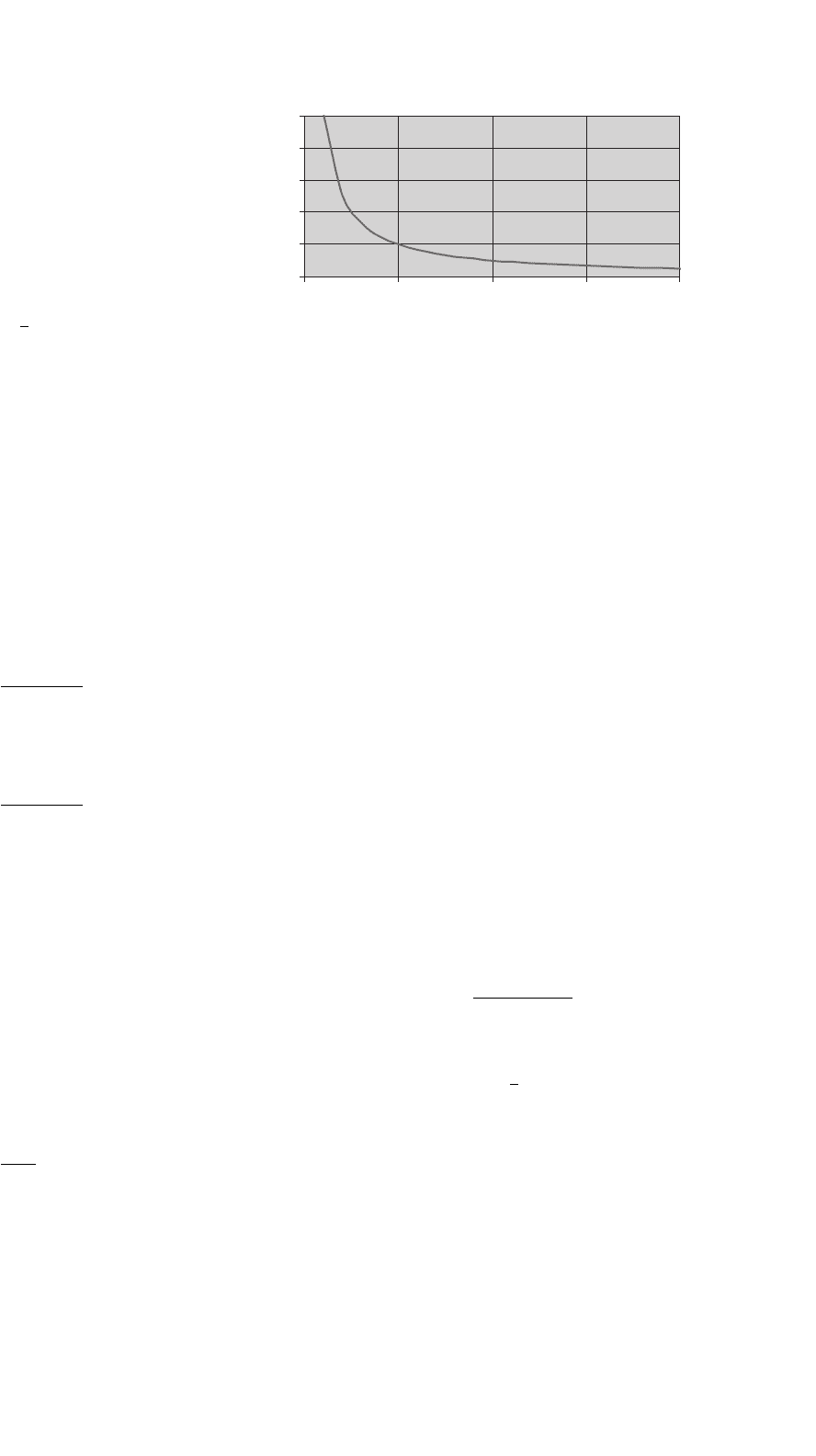
0
5
10
15
20
25
0% 5% 10% 15% 20%
DC Bus Voltage Ripple (%)
Capacitance (p.u.)
FIGURE 17.32 Capacitance required as a function of the maximum
voltage ripple on dc bus.
the capacitance will decrease the amount of ripple in the dc
voltage. By assuming that each level has the same voltage V
dc
across it,
V
n
= %V
ripple
·V
dc
(17.39)
Figure 17.32 shows a graph of the required capacitance as a
function of the maximum permissible voltage ripple on the dc
link. The graph indicates that an unnecessarily strict tolerance
on the voltage ripple of the dc bus will result in extraordinarily
large capacitor values. For this reason, the maximum voltage
ripple is normally chosen to be in the 5–10% range.
The current that flows through the capacitor determines
the change in charge q
n
for a capacitor C
n
. This current is a
function of what input and output voltage states the inverter
progresses through each cycle, and will largely be dependent
on the control method implemented by the series and par-
allel inverter in maintaining the voltage on the dc link. In
addition, the current waveforms i
PI
and i
SI
also will depend
largely on the system conditions, in other words, the type of
compensation that the converter is conducting. Although the
current that flows through each capacitor C
n
that makes up
the dc link will be different, for the reasons mentioned previ-
ously in Section 17.4.2, normally each of the capacitors will be
identically sized such that Eq. (17.38) can then be rewritten as
C
n
= C
dc
=
max
q
n
%V
ripple
·V
dc
(17.40)
Suppose a UPFC is connected to a distribution system with
a voltage of 13.8 kV line–line (7970 V line–ground). From
Eq. (17.22), V
device
rating
· (m − 1) ≥
√
2 · 7970 · 1.5 = 16, 900 V.
If 3300 V IGBTs are chosen for the design, then the number of
levels m would be 6. The next lower rating of available IGBTs is
2500 V, and use of these devices would require 7 levels. Because
of the added complexity and computational burden of 7 levels,
the design with 6 levels of 3300 V IGBTs is chosen.
A 13.8 kV line–line ac waveform from an inverter requires a
minimum dc link voltage of approximately 11.3 kV. The nom-
inal dc voltage for each level would be approximately 2000 V.

478 S. Khomfoi and L. M. Tolbert
TABLE 17.7 Back-to-back MUPC clamping diode ratings
Per unit
voltage
rating
Blocking
voltage
required
Voltage rating
of diode used
Number of
diodes per leg
Total number
per phase
1V
dc
3000 V 3000 V 1 2
2V
dc
6000 V 3000 V 2 4
3V
dc
9000 V 3000 V 3 6
4V
dc
12,000 V 3000 V 4 8
For a design factor of 1.5, the design voltage for each level of
the inverter would be approximately 3000 V.
From Eq. (17.23), the minimum total voltage block-
ing capability for a back-to-back converter would be,
V
clamp
total
= 6 ·(6 −2) ·(6 −1) ·3000 V = 360 kV. Each phase
of the converter will require the blocking voltages shown in
Table 17.7.
The current rating of the active devices in the series inverter
is found from Eq. (17.31)
I
SI
device
rating
=
20 MVA ·
(1/1 −0.3) −1
√
3 ·13, 800 V
·1.5 = 540 A
The current rating of the active devices in the parallel
inverter is found from Eq. (17.35):
I
PI
device
rating
=
20 MVA ·
1 −0.85
2
1/2
√
3 ·13, 800 V
·1.5 = 661 A
Use of 3300 V, 800 A IGBTs would be sufficient for both the
series and parallel inverter.
The current rating of the clamping diodes in the series
inverter is found from Eq. (17.36)
I
SI
clamping
diode
=
540 A
2 ·
(
6 −1
)
= 54 A
Likewise, the current rating of the clamping diodes in the
parallel inverter is found from Eq. (17.37)
I
PI
clamping
diode
=
660 A
2 ·
(
6 −1
)
= 66 A
Use of 3000 V, 75 A diodes would be sufficient for both the
series and parallel inverter.
17.5 Fault Diagnosis in Multilevel
Converters
Since a multilevel converter is normally used in medium to
high power applications, the reliability of the multilevel con-
verter system is very important. For instance industrial drive
applications in manufacturing plants are dependent upon
induction motors and their inverter systems for process con-
trol. Generally, the conventional protection systems are passive
devices such as fuses, overload relays, and circuit breakers to
protect the inverter systems and the induction motors. The
protection devices will disconnect the power sources from the
multilevel inverter system whenever a fault occurs, stopping
the operated process. Downtime of manufacturing equipment
can add up to be thousands or hundreds of thousands of dol-
lars per hour, therefore fault detection and diagnosis is vital
to a company’s bottom line. In order to maintain continuous
operation for a multilevel inverter system, knowledge of fault
behaviors, fault prediction, and fault diagnosis are necessary.
Faults should be detected as soon as possible after they occur,
because if a motor drive runs continuously under abnormal
conditions, the drive or motor may quickly fail.
The possible structure for a fault diagnosis system is illus-
trated in Fig. 17.33. The system is composed of four major
states: feature extraction, neural network classification, fault
diagnosis, and switching pattern calculation with gate sig-
nal output. The feature extraction performs the voltage input
signal transformation, with rated signal values as important
features, and the output of the transformed signal is trans-
ferred to the neural network classification. The networks are
trained with both normal and abnormal data for the multi-
level inverter drive (MLID) thus, the output of this network is
nearly 0 and 1 as binary code. The binary code is sent to the
fault diagnosis to decode the fault type and its location. Then,
the switching pattern is calculated to reconfigure the multilevel
inverter.
Switching patterns and the modulation index of other active
switches can be adjusted to maintain voltage and current in a
balanced condition after reconfiguration recovers from a fault.
The MLID can continuously operate in a balanced condition,
of course, the MLID will not be able to operate at its rated
power. Therefore, the MLID can operate in balanced condi-
tion at reduced power after the fault occurs until the operator
locates and replaces the damaged switch [74].
17.6 Renewable Energy Interface
Multilevel converters can be used to interface with renew-
able energy and/or distributed energy resources because several
batteries, fuel cells, solar cells, wind turbines, and micro tur-
bines can be connected through a multilevel converter to